Abstract
In this minreview, we summarize recent progress in the synthesis, properties and applications of a new type of one-dimensional nanostructures — single crystalline porous silicon nanowires. The growth of porous silicon nanowires starting from both p- and n-type Si wafers with a variety of dopant concentrations can be achieved through either one-step or two-step reactions. The mechanistic studies indicate the dopant concentration of Si wafers, oxidizer concentration, etching time and temperature can affect the morphology of the as-etched silicon nanowires. The porous silicon nanowires are both optically and electronically active and have been explored for potential applications in diverse areas including photocatalysis, lithium ion battery, gas sensor and drug delivery.
Introduction
Porous silicon has attracted a great deal of interest for the past two decades due to its remarkable chemical and physical properties.1–20 The porous silicon with highly efficient visible photo- and electro-luminescence has been explored to develop silicon-based optoelectronic devices.1–3,5,12,16 Combination of the optical properties and biodegradable and biocompatible features of porous silicon has stimulated the biomedical applications,4,17,21,22 such as drug delivery system, tissue engineering scaffolds, biosensors and biomarkers. Porous silicon also shows a variety of other interesting properties, including tunable refractive index, high internal surface, variable surface chemistry, and high chemical reactivity. All these properties make it an interesting material for potential applications in a wide range of fields, such as optics, electronics, optoelectronics, chemical sensors, renewable energy, lithium ion battery and biology.1–22
One-dimensional silicon nanostructures have been broadly explored for nanoscale electronics,23,24 flexible large area electronics,25–29 thermoelectrics,30 photovoltaics,31–35 battery electrodes,36 and biosensors.37,38 However, they can hardly be used as an optically active material for functional optoelectronics due to the nature of indirect band gap of silicon. On the other hand, silicon quantum dots and porous silicon are well-known for their ability to exhibit visible photo- or electro-luminescence due to strong quantum confinement effect or surface defects.2,39,40 Recent reports of single crystalline porous silicon nanowires have combined these two features together and form both electrically and optically active silicon nanostructures.41–51 The development of these multifunctional nanostructures may open new opportunities for a new generation of silicon based optoelectronics and photoelectrochemical devices. In this articles, we highlight recent progress in the synthesis of porous silicon nanowires, optical and electric properties, as well as their potential applications in the fields of energy and biology.
Synthesis of Porous Silicon Nanowires and the Mechanism
In general, porous silicon is produced by anodic etching in hydrofluoric (HF)-containing aqueous or organic solutions2 or by chemical etching in nitric acid/hydrofluoric (HNO3/HF) solution.52 A simple metal-assisted chemical etching method was developed to produce porous silicon with excellent and repeatable optical properties.2 Lately, this method was also adapted to synthesize vertical silicon nanowire arrays in an etchant solution composed of HF and a selected oxidant (hydrogen peroxide (H2O2) and metal salts, such as AgNO3, KAuCl4, K2PtCl6)53–57. This method has been widely studied for the synthesis of silicon nanowires starting from various types of silicon wafers with different doping levels and orientations, including lightly and highly doped p-type Si(100) and Si(111) wafers, lightly doped n-type Si(100) and Si(111) wafers and Si(110) and Si(113) wafers.41–51,53–58 The metal-assisted chemical etching reactions can be classified into two types: one-step reaction and two-step reaction. Recent reports show that single crystalline porous silcion nanowires have been synthesized through both one-step and two-step reactions by adjusting the reaction conditions.41–51
Highly Doped p-type Si (100) Wafer43
One-step chemical etching involves the immersion of clean p-type silicon substrates in an etchant solution containing 0.01–0.04 M AgNO3 and 5 M HF. It was found that the surface morphology of the as-synthesized silicon nanowires was highly dependent on the resistivity of the original silicon wafers. Rough surfaced silicon nanowires were observed when lightly doped silicon wafer (10 Ω·cm) was used. Porous silicon nanowires were obtained from silicon wafer with a resistivity of less than 0.005 Ω·cm. As grown silicon nanowires were vertically oriented on silicon substrate as shown in Fig 1a. The transmission electron microscopy (TEM), the selected area electron diffraction (SAED) (Fig. 1b) along with the high resolution transmission electron microscopy (HRTEM) (Fig. 1c, 1d) studies indicate that the resulting porous silicon nanowires maintain the single crystalline structure and axial orientation of the starting silicon wafer. The observed increase in the surface roughness and porosity with decreasing resistivity can be a result of high dopant concentration of silicon wafers. Details of mechanism for pore formation are further discussed below.
Fig. 1.
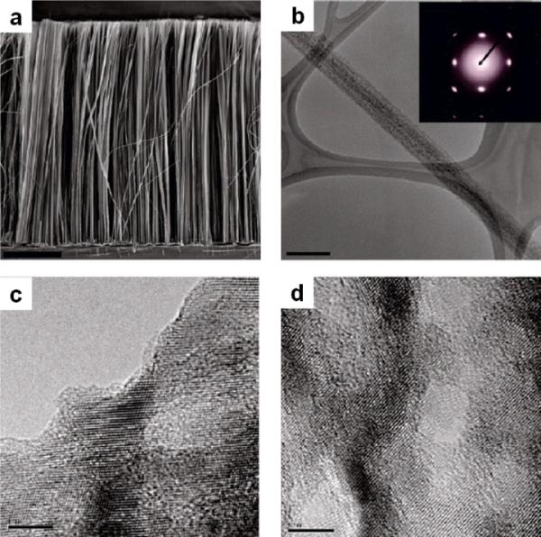
Structural characterization of the porous silicon nanowires synthesized from highly doped p-type Si wafers (0.005 Ω·cm). (a) SEM image of the cross section of the as-etched porous silicon nanowires. (b) TEM image of a typical porous silicon nanowire from which the SAED 15 (inset) pattern was obtained. (c, d) Phase contrast TEM images of the silicon lattice around pores near the surface and in the interior of the nanowire. The scale bar is 10 μm for a, 200 nm for b, and 5 nm for c and d. (Adapted from ref. 43. Copyright 2009 American Chemical Society.)
Highly Doped n-type Si (100) Wafer42
Two-step metal assisted electroless chemical etching method is adopted to grow silicon nanowire arrays from heavily doped n-type silicon wafers. The etching process involves chemical deposition of silver metal on silicon substrate in a solution composed of 0.005 M AgNO3 and 4.8 M HF for 1 minute followed by electroless etching in an etchant solution containing various concentrations of H2O2 and 4.8 M HF. Extensive studies show that the concentration of H2O2 and doping level of silicon wafer are main factors to control morphology of the as-synthesized silicon nanowires.42,46 The investigation of the concentration of H2O2 was carried out on silicon wafer with a resistivity of 0.008 – 0.02 Ω·cm. SEM and TEM images of the as-grown silicon nanowires from the highly doped n-Si (100) wafers with different concentrations of H2O2 are summarized in Fig. 2. For 0.1 M H2O2, nonporous nanowires were obtained as shown in TEM images Fig. 2b and 2d for 30 and 60 minute reations, respectively. With increasing H2O2 concentration, the silicon nanowires become increasingly rough on the surface, then start to evolve porous shells surrounding the solid cores, and eventually form entirely porous nanowires. For the 30 minute reaction, starting from H2O2 of 0.1 to 0.15, 0.2, and 0.3 M, the resulting nanowire evolves from pure solid nanowires (Fig. 2b) to rough-surfaced nanowires (Fig. 2f), solid/porous core/shell nanowires (Fig. 2j), and porous nanowires (Fig. 2n). For the 60 minute reaction, the resulting nanowires follow the same trend only with thicker porous layer for the respective reactions. These studies clearly demonstrate that the increase portion of the nanowires becomes porous with the increase of the H2O2 concentration and reaction time. Fig. 3 shows the HRTEM and SAED (inset) patterns from the as-grown silicon nanowires with 0.1 M H2O2 for 30 minute reaction, 0.2 M H2O2 for 30 mintue reaction, and 0.3 M H2O2 for 60 minute reaction, respectively. The continuous lattice fringes and the single crystal-like diffraction pattern are observed in all samples, demonstrating that both the nonporous and nanoporous silicon nanowires retain the single crystalline structure of the starting silicon wafer. These studies indicate that the etching process did not destroy the crystalline integrity of the structure.
Fig. 2.
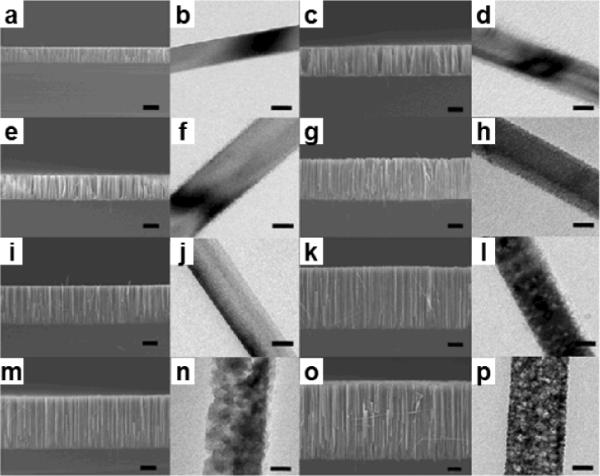
SEM and TEM images of silicon nanowire morphology from n-Si(100) with 0.008–0.02 Ω·cm resistivity in etchant solutions composed of 4.8 M HF and variable concentrations of H2O2 through a two-step reaction. (a,b) 0.1 M H2O2 for 30 min; (c,d) 0.1 M H2O2 for 60 min; (e,f) 0.15 M H2O2 for 30 min; (g,h) 0.15 M H2O2 for 60 min; (i,j) 0.2 M H2O2 for 30 min; (k,l) 0.2 M H2O2 for 60 min; (m,n) 0.3 M H2O2 for 30 min; and (o,p) 0.3 M H2O2 for 60 min. The scale bars for all SEM and TEM images is 10 μm and 60 nm, respectively. (Adapted from ref. 42. Copyright 2009 American Chemical Society.)
Fig. 3.
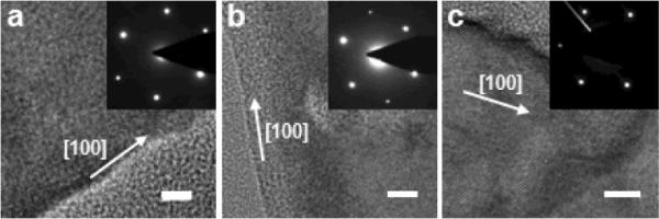
High-resolution TEM images with SAED patterns of nonporous and porous silicon nanowires. (a) Nanowires obtained from the reaction in 0.1 M H2O2 and 4.8 M HF for 30 min. (b) Nanowires obtained from the reaction in 0.2 M H2O2 and 4.8 M HF for 30 min. (c) Nanowires obtained from the reaction in 0.3 M H2O2 and 4.8 M HF for 60 min. All the scale bars are 5 nm. (Adapted from ref. 42. Copyright 2009 American Chemical Society.)
Lightly Doped Si (100) Wafer
It is also possible to achieve single crystalline porous silicon nanowires starting from lightly doped Si(100) wafer by controlling the etching conditions. Chen et.al. reported the formation of porous silicon nanowires (1–10 Ω cm) using etchant solution composed of HF, AgNO3 and H2O2 at different temperatures47. In the absence of H2O2, porous silicon nanowires could not be produced at reaction temperature below 50 °C. The addition of H2O2 into the etchant facilitates the increase of pore density as shown in Fig. 4. Porous silicon nanowires starting from p-type Si(100) wafer with a resistivity of 1–100 Ω cm have been also reported using one step reaction by adjusting the etching temperature and duration, AgNO3 concentration, and the amount of etching solution.50
Fig. 4.
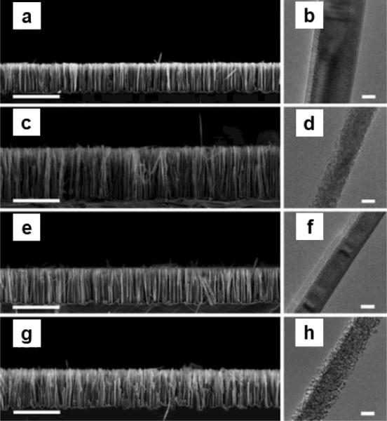
SEM and TEM images porous silicon nanowires etched from n-Si (100) with a resistivity of 1–10 Ω cm at different temperature, time and H2O2 concentrations. (a, b) 0 M H2O2, 60 min, 60 °C; (c, d) 0.3 M H2O2, 60 min, 60 °C; (e, f) 0 M H2O2, 40 min, 80 °C; (g, h) 0.3 M H2O2, 40 min, 80 °C. Scale bars for SEM and TEM images are 10 μm and 50 nm. (Adapted from ref. 47. Copyright 2011 Royal Chemical Society.)
Porosity
Generally, the porosity of porous silicon nanowires increases with increasing concentration of oxidizer (H2O2), conductivity of the starting Si wafer and etching time.42,46,48 A recent systematic study indicates the porosity and specific surface area of the as-synthesized silicon nanowires are tunable by controlling reaction conditions and resistivity of starting Si wafers.46 For the reaction time of 30 minutes in an etching solution of 0.3 M H2O2 and 4.8 M HF, the surface areas are 30, 40, 240, 370 m2 g−1 for silicon nanowires synthesized from Si wafers with resitivities of 1–5, 0.3–0.8, 0.008–0.016 and 0.001–0.002 Ω·cm, respectively (Fig. 5a). The total pore volumes are 0.05, 0.06, 0.47 and 0.65 cm3/g at P/P°= 0.90 for silicon nanowires abtianed from Si wafers with the resistivities of 1–5, 0.3–0.8, 0.008–0.016 and 0.001–0.002 Ω·cm, respectively. Fig. 5b shows the nitrogen adsorption/desorption isotherms of porous silicon nanowires synthesized from Si wafer (0.008–0.016 Ω·cm) in etching solution composed of 0.3 M H2O2 and 4.8 M HF for various times. The surface areas are increased from 160 m2 g−1 to 240 and 337 m2 g−1 for 15, 30 and 60 minute etching, respectively.
Fig. 5.
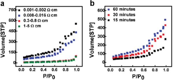
Nitrogen adsorption/desorption isotherms of as-synthesized silicon nanowires obtained (a) from Si wafers with various resistivities for 30 min etching in 0.3 M H2O2 and 4.8 M HF and (b) from 0.008–0.016 Ω· cm Si wafer for various etching times. (Adapted from ref. 46. Copyright 2011 American Chemical Society.)
Mechanism of Pore Formation
The formation of silicon nanowire array is via a nanoelectrochemical reaction process that is confined to location near Ag nanoparticles. The chemical reactions for one-step and two-step etching processes are listed as the following:
- One-step reaction
- Two-step reaction
For formation of porous silicon nanowires using one-step etching process on the highly doped p-type Si wafers, dopants, as crystal defects or impurities in silicon are suggested to serve as nucleation sites for pore formation. Higher concentration of dopants in wafers with lower resistivities provides more nucleation spots and lowers the energy barriers for charge transfer between silicon substrate and Ag metal.43 As a result, higher dopant concentrations may create a larger thermodynamic driving force for pore formation. In this process, Ag+ ions play dual roles as the oxidizer and the source for the formation of etching co-catalysts Ag metal.
In the two-step chemical etching for highly doped Si wafers (n-type),42, 46 the silver nanoparticle catalysts are predeposited on the clean silicon surface. Since H2O2 itself cannot etch the silicon, the formation of porous structures need to be facilitated by the metal nanoparticles. Previous studies suggested that the silver nanoparticles could be oxidized into Ag+ ion53 during the etching process as follows:
In a typical etch process, the silver particles are partially oxidized by H2O2 to create a localized Ag+ cloud in the close proximity of the silver particles. Silver ions can quickly react with silicon and take electrons from silicon near the Ag/Si interface and be recovered into original silver particles again. In this way, the etching is localized around the silver nanoparticles and the silver nanoparticles are trapped in the nanopits created by themselves, leading to continued etching in the vertical direction and the formation of vertical silicon nanowire array. However, as the H2O2 concentration increases, the concentration of Ag+ ion increases.42,46 In this case, the Ag+ ions may not be 100% recovered into the original silver nanoparticles and some of them may diffuse out. When the amount of the out-diffused Ag+ ions reach a certain threshold, they may nucleate on the side wall near defective sites (e.g., around the dopants) by extracting electrons from the silicon nanowires and forming new silver nanoparticles as a new etching pathway along the lateral direction of the nanowires. In this way, the higher H2O2 concentration increases the amount of out-diffused Ag+, and the increase of doping concentration increases the amount of weak defective points in the silicon lattice; both are important factors for the initiation of additional etching pathways in addition to the vertical etch, which explains the observation of the increased porosity with increasing H2O2 concentration during the etching of highly doped n-Si wafers. Meanwhile the nanowires from lightly doped silicon wafers have few defective sites so that there is less chance for out-diffused Ag+ ions to nucleate on the sidewalls. The cross section SEM images of as-synthesized silicon nanowire arrays without nitric acid washing indicate clean surface of silicon nanowires from 1–5 Ω·cm and 0.3–0.8 Ω·cm silicon wafers (Fig. 6a, 6b). In contrast, nanowires from two highly doped wafers (Fig. 6c, 6d) show rough surfaces with large numbers of small nucleated Ag nanoclusters. Those newly nucleated Ag nanoclusters can serve as new etching sites, which may lead to the formation of pores on the sidewalls of silicon nanowires.
Fig. 6.
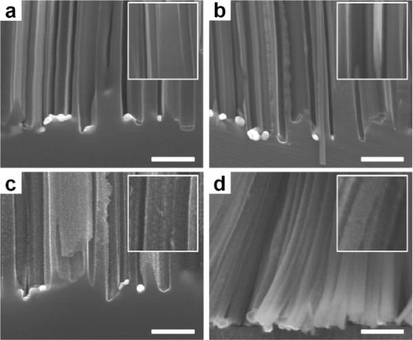
Cross-sectional SEM images of silicon nanowires etched from four n-type wafers with various resistivities for 15 min in the etchant solutions containing 0.3 M H2O2 with nitric acid treatment. (a) 1–5 Ω · cm; (b) 0.3–0.8 Ω · cm; (c) 0.008–0.016 Ω · cm; and (d) 0.001–0.002 Ω · cm. Scale bars is 500 nm. (Adapted from ref. 46. Copyright 2011 American Chemical Society.)
For porous silicon nanowires generated from lightly doped Si wafers, the growth conditions are similar to those from heavily doped Si wafers except the requirement of higher oxidizer concentration or elevated temperature.47,49 Although the detailed mechanism is not clear for pore formation on lightly doped Si wafer, higher concentration of oxidizer and higher reaction temperature played siginificant roles during etching process.
Another recent work reports the formation of porous silicon nanwires regardless of silicon resistivity using two-step reactions.45 Silicon resistivity, H2O2 concentration, and ethanol concentration are key etching parameters for the formation of solid nanowires, porous nanowires, porous silicon layer, porous silicon nanowires on porous silicon layer and polished silicon surface. In this work, the metal ions rather than metal nanoparticles are proposed to be responsible for the pore formation since no metal nanoparticles are detected within the pores of silicon nanowires. The main difference of this study to ref. 41 and 44 is the existence of surfactant ethanol, which may be responsible for the different observations and interpretations.
Two more recent studies reported the synthesis of regular array of (porous) silicon nanowire using bilayer-Au/Ag or single-layer-Au nanomesh catatlyst on the p-Si(100) wafers (1–10 Ω·cm), and offered some additional insights into the pore formation mechanism.59,60 In th case of bilayer-Au/Ag catalyst, Au is believed to be chemically inert against the mixture of HF and H2O2 and function as the catalyst for H2O2 decomposition, while the Ag metal acts as the catalyst for the oxidation of silicon. In general, the resulting nanowires exhibit uniform diameters along nanowire axis, suggesting little metal dissolution during the etching process. Therefore, an alternative mechanism based on holes injection and diffusion in silicon are proposed to explain the pore formation in the silicon nanowires.59 Within this argument, at low concentration of H2O2, a relative small number of holes (h+) are generation on the metal catalysts and injected into silicon and the oxidation and etching of silicon are localized at the interface between silicon and Ag metal. With a high concentration of H2O2, the rate of generation and injection of holes into silicon are accelerated at silicon and silver interface. If the HF concentration is too low to remove the oxide in time for continued oxdiation and consumption of the all holes, the extra holes may diffuse away from the interface to crystal defects and dopant sites on the surface of the already formed silicon nanowires, leading to the nucleation of new etching pathway and the formation of pores on silicon nanowires.
The above discussions clearly demonstrate that the formation of porous silicon nanowires highly depends on the etching conditions. More efforts are necessary to understand the growth mechanism and to achieve the porous silicon nanowires with predictable and controllable porosity.
Optical Properties
The optical properties of the resulting porous silicon nanowires are probed in bulk solution and in individual nanowires dispersed on glass substrate or TEM grid in previous investigations. The porous silicon nanowires synthesized from highly doped Si wafers show a broad visible emission centered around 680 nm (Fig. 7a) and 650 nm (Fig. 7b) for p-type and n-type, respectively.42,43 The visible emission may be originated from the deep quantum confinement in the porous structure, and the broad emission may be attributed to broad size distribution of the critical dimensions in the porous silicon nanowire structures. Other factors such as surface trap states may also contribute to the broad photoluminescence emission. The corresponding fluorescence image overlaps with the microscopy image (Fig. 7d, 7e), confirming the photoluminescence is indeed originated from the porous silicon nanowires. Porous silicon nanowires generated from lightly doped Si wafer emit a strong green emission with the band centerd at 560 nm (Fig. 7c).47 Though such a big blue shift was attrbuted to the lightly doping level of Si wafer, an exact mechanism needs to be further explored.
Fig. 7.
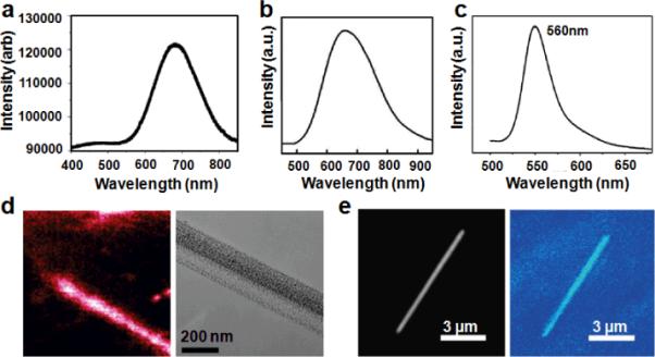
Optical properties of porous silicon nanowires. Photoluminescence spectrum of porous silicon nanowires synthesized from (a) 0.005 Ω · cm p-type Si(100); (b) 0.008–0.02 Ω · cm n-type Si(100) wafer; and (c) 1–10 Ω · cm n-type Si(100) wafer. (d) Overlap between confocal photoluminescence image and electron microscopy image for sample in a. (e) Overlap between confocal photoluminescence image and optical microscopy image for sample in b. (a, b, d, and e adapted from ref. 42,43. Copyright 2009 American Chemical Society. c adapted from ref. 47. Copyright 2011 Royal Chemical Society.)
Detailed investigations on the photoluminscence of porous silicon nanowires suggest that the intensity of photoluminscence can be effectively enhanced with increasing porosity.48 The as-synthesized porous silicon nanowires always show a nearly symmetrical photoluminscence spectrum (Fig. 8a). However, HF-treated porous silicon nanowires display an asymmetrical photoluminscence with a red-shfit, indicating the photoluminscence spectrum has two origins: surface Si-H and Si-O bonds. Si-H bonds cause the red-shift of photoluminscence spectrum (Fig. 8b).48 Selenization of porous silicon nanowires over 700 °C results in a blue-shift in photoluminscence spectrs with an asymmetrical pattern.49 The decomposition of photoluminscence spectra indicates three independent peaks at 595, 645 and 715 nm (Fig. 8d). The peak at 715 nm is close to that of porous silicon nanowire without selenization and could be originated from the surface silicon oxide layer. The 595 nm and 645 nm peaks arise from the surface Si-Se speices. The longer annealing time during selenization process facilitates the diffusion of Se to form more surface Si-Se bonds. Therefore, it can dramatically enhance the photoluminscence singal of porous silicon nanowires. A factor over 30 is achieved for 5 hour annealing as shown in Fig. 8c.
Fig. 8.

Photoluminscence spectra of porous silicon nanowires from Si wafer (0.02 Ω·cm) before amd after selenium treatment. (a) Porous silicon nanowires etched in presence of 0.3 M H2O2 for 30, 60, 90, 120 and 180 min after HF treatment for sample 1–5, respectively. (b) The deposition of photoluminscence spectrum of sample 5 in (a). (c) The Photoluminscence of porous silicon nanowires after selenium treatment. (d) The deposition of photoluminscence spectrum of porous silicon nanowires after 5 hr 700 °C Se-treatement in (c). (a and b adapted from ref 48. Copyright 2011 Springer. c and d adapted from ref. 49. Copyright 2011 Institute of Physics.)
Electronic Properties
Electrical transport studies on individual porous silicon nanowires prepared from n-type Si(100) wafer with a resistivity of 0.008–0.02 Ω cm was conducted on a silicon substrate, where an underlying silicon was used as the back gate, 100 nm thick silicon nitride (SiNx) as the gate dielectric, and Ti/Au (100 nm/50 nm) film deposited using an e-beam evaporator as the source and drain electrodes. A typical fabricated device is shown in Fig. 9a. Fig. 9b shows a typical set of drain current versus drain bias voltage (Id-Vd) relations at various gate voltages (Vg) in steps of 5 V for a porous silicon nanowire device. These electrical characterizations show that the channel conductance increases when applying positive gate voltages and decreases with negative gate voltages, suggesting an n-channel transistor behavior, which is consistent with the doping type of the starting Si wafer.42 However, this inirial study suggests that the overall resistance of the porous silucon nanowires is rather large compared to that of solid silicon nanowire of similar dimension and the starting doping concentration. The reduced conductance may be attributed to several factors including the reduced current conducting volume, surface depletion layer and preferential etching removal of dopants. Considering the large surface area, the electronic properties of the porous silicon nanowires can be readily tuned with proper surface chemistry to reduce the surface depletion or induce surface doping effect. It can therefore open the exicting opportunities for the design of novel types of devices for electronics, optoelectronics, or chemical biological sensors.
Fig. 9.
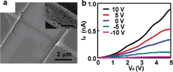
(a) SEM image of a porous silicon nanowire device. The scale bar of inset is 100 nm. (b) Drain current versus drain voltage at variable gate voltage (Adapted from ref. 42. Copyright 2009 American Chemical Society.)
Applications
Applications of electronically and optically active porous silicon nanowires have been explored in the field of photocatalysis, gas sensor, lithium battery and drug delivery. In this section, we summarize a few examples below.
Photocatalysis44
Porous silicon nanowires obtained through a metal-assisted electroless wet chemical etching approach exhibit a broad visible emission centered near red-infrared wavelength, suggesting excitons generated within the porous SiNWs could be energetic enough to drive applicable photoelectrochemical reactions.42,43,48,49 Compared to TiO2, the overall absorption of the porous silicon nanowires is much broader as it spans over the entire spectral range from UV to visible and near infrared (IR). Therefore, porous silicon nanowires can be an interesting cadidate for future photocatalytic applications.
PtNPs with 3–4 nm diameters were incorporated onto porous silicon nanowires to enhance the photocatalytic activity because the difference in their Fermi levels can introduce a Schottky barrier between the Pt and porous silicon nanowires. The built-in potential within the Schottky barrier can facilitate the separation of photogenerated electron-hole pairs. Futhermore, properly selected metal nanoparticles can also function as the catalysts to facilitate certain redox reactions.
The photocatalytic activity of the porous silicon nanowires (Fig. 10a) and PtNP loaded porous silicon nanowires (Fig. 10b PtNPs-pSiNWs) is compared for the photocatalytic degradation of indigo carmine (IC) (Fig. 10c) and photodegradation of 4-nitrophenol (Fig. 10d). After 60 minutes of irradiation, the percentages of degraded IC are 37.2% and 86.9% for porous silicon nanowires and PtNP-pSiNW, respectively. In contrast, only 4.7 % of IC molecules were degraded with the same irradiation conditions without the PtNP-pSiNW photocatalysts. The results clearly demonstrate that porous silicon nanowires can function as effective photocatalysts in the visible irradiation range and that the Pt-loaded porous porous silicon nanowires are much more efficient photocatalysts than the porous SiNWs only. This catalytic enhancement by PtNPs could be attributed to their ability to facilitate electron-hole separation and to promote electron transfer process in catalytic photodegradation reaction. The photodegradation of 4-nitrophenol displays a similar catalytic behavior (Fig. 10d).
Fig. 10.
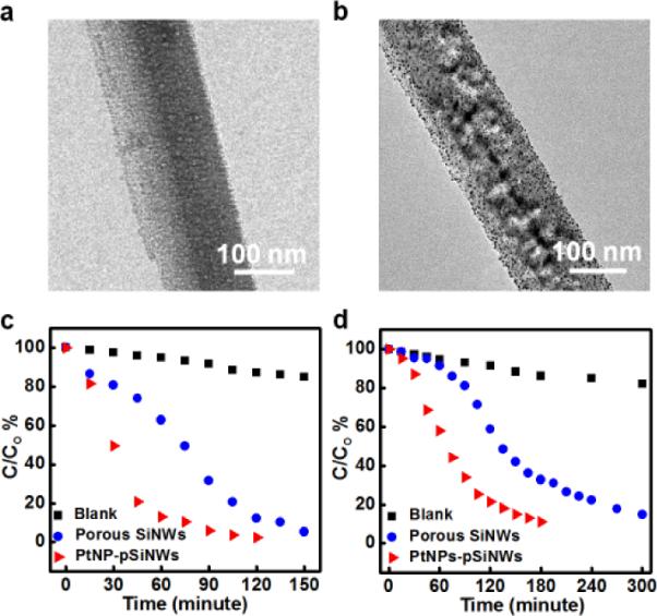
(a) TEM image of a porous silicon nanowire. (b) TEM images of PtNP-pSiNW catalyst. (c) IC degradation catalyzed by the porous silicon nanowires and Pt loaded porous silicon nanowires. The concentration of all catalysts was set at 0.3 mg/ml. (d) 4-nitrophenol degradation catalyzed by the porous silicon nanowires and PtNP loaded porous silicon nanowires. (Adapted from ref. 44. Copyright 2011 Royal Chemical Society.)
Drug Delivery Carriers51
Particles of porous silicon with attractive properties of high surface area, intrinsic luminescence and bio-degradability may function as a very promising scaffold for delivering drugs. To this end, porous silicon nanorods with length ranging from 200 nm to 400 nm were synthesized by sonication breaking down porous silicon nanowires. The prorous Si nanorods can then serve as an delivery platform in biological systems to open new possibilities for drug delivery. The delivery system is established by coupling with a pH-responsive nanovalve-system consisting of an aromatic amino group and a cyclodextrin cap as illustrated in Fig. 11a.
Fig. 11.
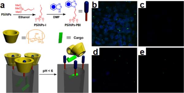
(a) Schematic illustration of pH-operated mechanism of the nanovalves. Confocal images of PANC-1 cells incubated with porous silicon nanorods: (b) Cells treated with 20 μg/ml of FITC-PSiNPs loaded with Hoechst 33342 at 37 °C. (c) Same experiment conducted at 4 °C No staining was observed after incubation at low temperature. (d) and (e) Competition tests: cells were treated with 20 μg/ml of FITC-PSiNPs loaded with Hoechst 33342 and (d) 60μg/ml and (e) 200μg/ml of plain PSiNPs at 37 °C. (Adapted from ref. 51. Copyright 2011 American Chemical Society.)
To create this mechanized delivery system with porous silicon nanostructures, the nanorods were first modified with 3-iodopropyl trimethoxysilane and then coupled with a benzimidazole molecule. The fluorescent biological staining dye Hoechst 33342 was then loaded into pores as a model cargo to investigate the delivery efficiency. The nanovalve, beta-cyclodextrin, was lastly added to finish the assembly of the delivery platmform. Under neutral pH conditions, the benzimidazole stalk remains hydrophobic and therefore can bind to the cyclodextrin molecule via supramolecular interactions. Thus, the bulky cyclic cyclodextrin molecules block the pore openings and function as gate keepers to prevent the leakage of cargo. When the pH is lowered, the benzimidazole is protonated, and the binding between the stalk and the cyclodextrin drops dramatically, resulting in an out-diffusion of the cargo. The studies on human pancreatic carcinoma PANC-1 cells further proved that the nanovalve-modified porous silicon nanorods can be taken up by cells and deliver their cargo inside them. Fig. 10b shows that after incubation for three hours, the Hoechst dye is released and stained the cell nucleus. Several control experiments as shown in Fig. 11c, 11d and 11e demonstrate that the nanovalves on the porous silicon nanorods do not open in cell culture medium at 37 °C, and also prove that the endocytosis process is necessary to enable the nanorods to reach lysosomes and trigger the release of the cargo.
Gas Sensors41
Silicon nanowires have been widely explored as biosensors and gas sensors. Electrically and optically active porous silicon nanowires with large porosity may open new opportunities for silicon-based sensor devices. Recently, a NO gas sensor based on n-type porous silicon nanowire array has been studied. The structure is illustrated in Fig. 12a, in which two deposited gold electrodes on the surface of porous silicon nanowire array work as the electrical contacts. Gas sensoring measurements are carried out within an air-tight chamber in a flow-through manner and are performed by monitoring the change of resistance of n-porous silicon nanowire array under different NO concentrations.
Fig. 12.

(a) Schematic illustration of porous silicon nanowire array as gas sensor device. (b) and (c) Dynamic electrical resistance response of porous silicon nanowires gas sensor to NO in dry air at room temperature. (Adapted from ref. 39. Copyright 2009 American Institute of Physics.)
The experiments indicate the device shows a shift response and recovery to low NO concenrtation as shown in Fig. 12b and 12c. For low concentration of NO@500 ppb, the response time are around 30 ~ 40 s, while the recovery time is around 60 s. The long response time is attributed to the high surface-to-volume ratio of porous silicon nanowires. For higher concentration of NO, the rate of recovery becomes slower due to the slower desorption of absorbed NO molecules from porous silicon nanowire surface. The mechanism of NO sensoring based on porous silicon nanowires is atrtibuted to the increasing of charge density within porous silicon nanowire upon NO absorption. The strong electron-donating nature of NO molecules leads to an increasing electron carriers and conductance of porous silicon nanowire array.
Lithuim Ion Battery50
Silicon has a theoretical Li storage capacity of 4200 mAh g−1, which is much higher than that of graphites (372 mAh g−1), the commerically available anode materials nowadays. Nanostructures can enhance the battery performance due to the more flexiblity to accomdate large swing in volume, short Li diffusion length for alloy and dealloy process and acceleration of charge transfer. Therefore, porous silicon nanostructures are potential anode materials for Li ion battery. A recent study shows enhanced Li storage capacity using porous silicon nanowires.50
The porous silicon nanowires are synthesized from p-type Si wafer with a resistivity of 1–100 Ω cm. The porous silicon nanowire electrode with the same content of carbon black exhibits five times higher initial capacities (2172 mAh g−1) than those of 56 nm silicon nanoparticles (477 mAh g−1). After 20 cycles, the capacity of porous silicon nanowires is 815 mAh g−1, which is 3.36 times higher than that of silicon nanoparticles. The enhanced capacity of porous silicon nanowire electrode is explained by their highly accessible surfaces and short diffusion length, resulting in more Si sources involving the reaction with Li. Kinetic study also indicates that porous silicon nanostructures enhance the electrochemical activity and results in a low energy barrier for alloying process.
Conclusions and Outlook
The present summary gives an overview of porous silicon nanowires including synthesis, formation mechanism, elelctrical and optical properites as well as their potential applications in diverse areas including photocatalysis, lithium ion battery, gas sensor and drug delivery. The synthesis of porous silicon nanowires is facile, predictable, controllable and scalable. The research to date has already stimulated significant interest for both fundamental investigations as well as potential technological applications. With the increasing interest from the scientific and technological community, the porous silicon nanowires with well defined nanostructures may offer exciting potential in variety of directions including nanoscale optoelectronics (e.g. light-emitting diodes), energy (e.g. as an alternative silicon electrode for photoelectrochemical devices and supercapacitors, for application in silicon-based photovoltaic devices), and medecine (e.g. drug delivery, fluorescent biolabeling tag, and chemical and biological sensors).
Although significant advancements have been made in both synthesis and applications of porous silicon nanowires, there are still several fundamental challenges for future applications. First, the mechansim of pore formation is still not fully understood. Further investigation of the growth mechansim will help improve the geometric structures of porous silicon nanowires with specific chemical and physical properties. Developing methods to rationally control the intrinsic porous characteristics of the porous silicon nanowires inlcuding pore size distribution and pore density is highly desirable for specific applications. The current synthesis approaches generally result in porous nanowires with a wide pore size distribution ranging from 2 nm to 20 nm. Narrow pore size distribution and controllable pore depth are important attributes for many applications such as catalysis and drug delivery. For example, for the drug delivery system discussed above, the cargo loading capacity in porous silicon nanorods is 5 times lower than that of mesoporous MCM-41 with pore size at 2.2 nm since the nanovalve only blocks small pores of porous silicon nanowires.51,61 Second, the surface chemistry of porous silicon nanowire remains largely unexplored. Rich surface chemistry can be explored on both silicon and silicon oxide, which can lead to imporant new functions on silicon surface for potential applications in the areas of sensors and biological systems. Passivation of the surface of porous silicon nanowires is also desired for some specific applications. For an example, the formation of native silicon oxide layer on the surface of porous silicon nanowires can block charge transportation and suppress the efficiency of solar energy conversion, which can be mitigated through proper surface passivation process. Surface passivation can also improve the stability of porous silicon nanowires in the biological systems and the harsh electrochemical solution in photocatalytic process. Third, future applications require a thorough understanding of the chemical and physical properties of porous silicon nanowires synthesized from both n- and p-type Si wafers with different dopants, doping levels and crystallographic orientations. Especially, optical and electric properties of porous silicon nanowire have only been studied on several types of silicon wafers. A systematic investigation will be desirable for future applications.
Notes and references
- 1.Kanemitsu Y. Phys. Rep.-Rev. Sect. Phys. Lett. 1995;263:1. [Google Scholar]
- 2.Cullis AG, Canham LT, Calcott PDJ. J. Appl. Phys. 1997;82:909. [Google Scholar]
- 3.Bisi O, Ossicini S, Pavesi L. Surf. Sci. Rep. 2000;38:1. [Google Scholar]
- 4.Stewart MP, Buriak JM. Adv. Mater. 2000;12:859. [Google Scholar]
- 5.Sailor MJ, Lee EJ. Adv. Mater. 1997;9:783. [Google Scholar]
- 6.Stalmans L, Poortmans J, Bender H, Caymax M, Said K, Vazsonyi E, Nijs J, Mertens R. Prog. Photovoltaics. 1998;6:233. [Google Scholar]
- 7.Yerokhov VY, Melnyk Renew. Sustain. Energy Rev. 1999;3:291. [Google Scholar]
- 8.Foll H, Christophersen M, Carstensen J, Hasse G. Mater. Sci. Eng. R-Rep. 2002;39:93. [Google Scholar]
- 9.Maex K, Baklanov MR, Shamiryan D, Iacopi F, Brongersma SH, Yanovitskaya ZS. J. Appl. Phys. 2003;93:8793. [Google Scholar]
- 10.Mizsei J. Thin Solid Films. 2007;515:8310. [Google Scholar]
- 11.Salonen J, Lehto VP. Chem. Engin. Jou. 2008;137:162. [Google Scholar]
- 12.Lockwood DJ. J. Mater. Sci. 2009;20:235. [Google Scholar]
- 13.Libertino S, Aiello V, Scandurra A, Renis M, Sinatra F, Lombardo S. Sensors. 2009;9:3469. doi: 10.3390/s90503469. [DOI] [PMC free article] [PubMed] [Google Scholar]
- 14.Boarino L, Borini S, Amato G. J. Electrochem. Soc. 2009;156:K223. [Google Scholar]
- 15.Korotcenkov G, Cho BK. Crit. Rev. Solid State Mater. Sci. 2010;35:153. [Google Scholar]
- 16.Torres-Costa V, Martin-Palma RJ. J. Mater. Sci. 2010;45:2823. [Google Scholar]
- 17.Martin-Palma RJ, Manso-Silvan M, Torres-Costa V. J. Nanophotonics. 2010;4 [Google Scholar]
- 18.Korotcenkov G, Cho BK. Rev. Solid State Mater. Sci. 2010;35:1. [Google Scholar]
- 19.Cho J. J. Mater. Chem. 2010;20:4009. [Google Scholar]
- 20.Kang ZH, Liu Y, Lee ST. Nanoscale. 2011;3:777. doi: 10.1039/c0nr00559b. [DOI] [PubMed] [Google Scholar]
- 21.Lin VSY, Motesharei K, Dancil KPS, Sailor MJ, Ghadiri MR. Science. 1997;278:840. doi: 10.1126/science.278.5339.840. [DOI] [PubMed] [Google Scholar]
- 22.Tasciotti E, Liu XW, Bhavane R, Plant K, Leonard AD, Price BK, Cheng MMC, Decuzzi P, Tour JM, Robertson F, Ferrari M. Nat. Nanotechnol. 2008;3:151. doi: 10.1038/nnano.2008.34. [DOI] [PubMed] [Google Scholar]
- 23.Cui Y, Duan XF, Hu JT, Lieber CM. J. Phys. Chem. B. 2000;104:5213. [Google Scholar]
- 24.Huang Y, Duan XF, Cui Y, Lauhon LJ, Kim KH, Lieber CM. Science. 2001;294:1313. doi: 10.1126/science.1066192. [DOI] [PubMed] [Google Scholar]
- 25.McAlpine MC, Friedman RS, Jin S, Lin KH, Wang WU, Lieber CM. Nano Lett. 2003;3:1531. [Google Scholar]
- 26.Duan XF. MRS Bulletin. 2007;32:134. [Google Scholar]
- 27.Javey A, Nam S, Friedman RS, Yan H, Lieber CM. Nano Lett. 2007;7:773. doi: 10.1021/nl063056l. [DOI] [PubMed] [Google Scholar]
- 28.Duan XF, Niu CM, Sahi V, Chen J, Parce JW, Empedocles S, Goldman JL. Nature. 2003;425:274. doi: 10.1038/nature01996. [DOI] [PubMed] [Google Scholar]
- 29.Duan XF. IEEE Trans. Electron Dev. 2008;55:3056. [Google Scholar]
- 30.Hochbaum AI, Chen RK, Delgado RD, Liang WJ, Garnett EC, Najarian M, Majumdar A, Yang PD. Nature. 2008;451:163. doi: 10.1038/nature06381. [DOI] [PubMed] [Google Scholar]
- 31.Tian BZ, Zheng XL, Kempa TJ, Fang Y, Yu NF, Yu GH, Huang JL, Lieber CM. Nature. 2007;449:885. doi: 10.1038/nature06181. [DOI] [PubMed] [Google Scholar]
- 32.Hwang YJ, Boukai A, Yang PD. Nano Lett. 2009;9:410. doi: 10.1021/nl8032763. [DOI] [PubMed] [Google Scholar]
- 33.Garnett EC, Yang PD. J. Am. Chem. Soc. 2008;130:9224. doi: 10.1021/ja8032907. [DOI] [PubMed] [Google Scholar]
- 34.Qu YQ, Xue T, Zhong X, Lin YC, Liao L, Choi JN, Duan XF. Adv. Funct. Mater. 2010;20:3005. doi: 10.1002/adfm.201000857. [DOI] [PMC free article] [PubMed] [Google Scholar]
- 35.Qu YQ, Liao L, Cheng R, Wang Y, Lin YC, Huang Y, Duan XF. Nano Lett. 2010;10:1941. doi: 10.1021/nl101010m. [DOI] [PMC free article] [PubMed] [Google Scholar]
- 36.Chan CK, Peng HL, Liu G, McIlwrath K, Zhang XF, Huggins RA, Cui Y. Nat. Nanotechnol. 2008;3:31. doi: 10.1038/nnano.2007.411. [DOI] [PubMed] [Google Scholar]
- 37.Zheng GF, Patolsky F, Cui Y, Wang WU, Lieber CM. Nat. Biotechnol. 2005;23:1294. doi: 10.1038/nbt1138. [DOI] [PubMed] [Google Scholar]
- 38.Patolsky F, Timko BP, Yu GH, Fang Y, Greytak AB, Zheng GF, Lieber CM. Science. 2006;313:1100. doi: 10.1126/science.1128640. [DOI] [PubMed] [Google Scholar]
- 39.Canham LT. Appl. Phys. Lett. 1990;57:1046. [Google Scholar]
- 40.Lin VSY, Motesharei K, Dancil KPS, Sailor MJ, Ghadiri MR. Science. 1997;278:840. doi: 10.1126/science.278.5339.840. [DOI] [PubMed] [Google Scholar]
- 41.Peng KQ, Wang X, Lee ST. Appl. Phys. Lett. 2009;95:243112. [Google Scholar]
- 42.Qu YQ, Liao L, Li YJ, Zhang H, Huang Y, Duan XF. Nano Lett. 2009;9:4539. doi: 10.1021/nl903030h. [DOI] [PMC free article] [PubMed] [Google Scholar]
- 43.Hochbaum AI, Gargas D, Hwang YJ, Yang PD. Nano Lett. 2009;9:3550. doi: 10.1021/nl9017594. [DOI] [PubMed] [Google Scholar]
- 44.Qu YQ, Zhong X, Li YJ, Liao L, Huang Y, Duan XF. J. Mater. Chem. 2010;20:3590. doi: 10.1039/c0jm00493f. [DOI] [PMC free article] [PubMed] [Google Scholar]
- 45.Chiappini C, Liu XW, Fakhoury JR, Ferrari M. Adv. Funct. Mater. 2010;20:2231. doi: 10.1002/adfm.201000360. [DOI] [PMC free article] [PubMed] [Google Scholar]
- 46.Zhong X, Qu YQ, Lin YC, Liao L, Duan XF. ACS Appl. Mater. Interf. 2011;3:261. doi: 10.1021/am1009056. [DOI] [PMC free article] [PubMed] [Google Scholar]
- 47.Chen HH, Zou RJ, Wang N, Sun YG, Tian QW, Wu JH, Chen ZG, Hu JQ. J. Mater. Chem. 2011;21:801. [Google Scholar]
- 48.Lin LH, Guo SP, Sun XZ, Feng JY, Wang Y. Nanoscale Res. Lett. 2011;5:1822. doi: 10.1007/s11671-010-9719-6. [DOI] [PMC free article] [PubMed] [Google Scholar]
- 49.Lin LH, Sun XZ, Tao R, Feng JY, Zhang ZJ. Nanotechnology. 2011;22:075203. doi: 10.1088/0957-4484/22/7/075203. [DOI] [PubMed] [Google Scholar]
- 50.Wang XL, Han WQ. ACS Appl. Mater. Interf. 2:3709. doi: 10.1021/am100857h. [DOI] [PubMed] [Google Scholar]
- 51.Xue M, Zhong X, Shaposhnik Z, Qu Y, Tamanoi F, Duan XF, Zink JI. J. Am. Chem. Soc. 2011;133:8798. doi: 10.1021/ja201252e. [DOI] [PMC free article] [PubMed] [Google Scholar]
- 52.Archer RJ. J. Phys. Chem. Solids. 1960;14:104. [Google Scholar]
- 53.Peng KQ, Yan YJ, Gao SP, Zhu and J. Adv. Mater. 2002;14:1164. [Google Scholar]
- 54.Zhang ML, Peng KQ, Fan X, Jie JS, Zhang RQ, Lee ST, Wong NB. J. Phys. Chem. C. 2008;112:4444. [Google Scholar]
- 55.Peng KQ, Xu Y, Wu Y, Yan YJ, Lee ST, Zhu J. Small. 2005;1:1062. doi: 10.1002/smll.200500137. [DOI] [PubMed] [Google Scholar]
- 56.Peng KQ, Zhu J. J. Electroanal. Chem. 2003;558:35. [Google Scholar]
- 57.Peng KQ, Hu JJ, Yan YJ, Wu Y, Fang H, Xu Y, Lee ST, Zhu J. Adv. Funct. Mater. 2006;16:387. [Google Scholar]
- 58.Huang ZP, Geyer N, Werner P, de Boor J, Gosele U. Adv. Mater. 2011;23:285. doi: 10.1002/adma.201001784. [DOI] [PubMed] [Google Scholar]
- 59.Kim J, Han H, Kim YH, Choi SH, Kim JC, Lee W. ACS Nano. 2011;5:3222. doi: 10.1021/nn2003458. [DOI] [PubMed] [Google Scholar]
- 60.Kim J, Kim YH, Choi SH, Lee W. ACS Nano. 2011;5:5242. doi: 10.1021/nn2014358. [DOI] [PubMed] [Google Scholar]
- 61.Meng H, Xue M, Xia T, Zhao YL, Tamanoi F, Stoddart JF, Zink JI, Nel AE. J. Am. Chem. Soc. 2010;132:12690. doi: 10.1021/ja104501a. [DOI] [PMC free article] [PubMed] [Google Scholar]


