

When the appropriate wavelength of light impinges on a noble metal nanostructure, it can cause the conduction electrons to oscillate collectively, resulting in localized surface plasmon resonance (LSPR) exciting.[1, 2] This process generates enhanced electromagnetic (EM) fields at the surface of the nanostructure that can be several orders of magnitude larger than the incident optical excitation fields,[2-6] leading to many types of surface enhanced phenomena,[3, 5, 7-14] including Surface Enhanced Raman Scattering (SERS). SERS has been extensively studied for several decades,[5, 15] and it is often described as a near-field phenomenon that occurs when the Raman molecules are in close proximity to the nanostructure’s surface, as the enhanced EM fields decay rapidly with distance from its surface.[15-17] The decay lengths have been reported to be in the range of a few nanometers and depend on the size, shape and composition of the nanostructure.[18, 19]
Recently, we developed a process termed On Wire Lithography (OWL)[20] for constructing nanostructures from one dimensional wires made via the template synthesis method.[21-24] OWL allows one to make rod and disk structures with sub-5 nm to many micrometer resolution. Importantly, it allows one to generate nanostructures made over different compositions adjacent to one another. Therefore, it allows one to probe important distance-dependent phenomena in many areas,[25, 26] including molecular electronics, catalysis, spectroscopy, and optics. Indeed, it is an excellent test-bed for probing some of the fundamental underpinnings of the SERS phenomenon.
In this communication, we describe how OWL can be used to fabricate nanostructures made of Au that have excitable plasmon resonances in the visible region of the spectrum (632.8 nm) and which are separated by nanometer scale distances from Ni segments that do not have such plasmon resonances but can be selectively modified with Raman-active probes. We have discovered that disk-like Au nanostructures can be separated from the Ni segments by 120 nm and still exhibit enhanced Raman scattering by the Raman probes, even though the probes are only localized on the Ni segment. This is an unprecedented example of long-range SERS. This long-range surface enhancement demonstrates a scheme for using plasmon excitation to enhance photoprocesses over distances that are relevant to applications in chemical and biological sensing.
In a typical experiment, OWL is used to fabricate a 360 nm diameter multisegmented nanowire containing: 1) a 1.5 μm segment of Au; 2) 1.5 μm gap; 3) a pair of 120 ± 18 nm long Au nanodisks that are separated by a 30 ± 10 nm gap (termed as Au nanodisk pair); and 4) a 1.5 μm Ni wire segment that is separated by a 120 ± 13 nm gap from the Au nanodisk pair (Figure 1a, left to right). The 120 nm Au disk thickness and 30 nm gap distance were chosen based upon previous results from our group which show that this is a near-ideal geometry for obtaining optimized EM enhancement in the context of pure gold structures (i.e. no Ni).[27]
Figure 1.
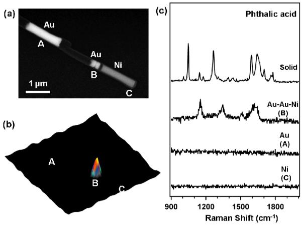
(a) Scanning electron microscopy image of Au-Ni multisegmented nanowires. Left to right: a 1.5 μm Au nanowire; a pair of 120 ± 18 nm long Au nanodisks (360 nm diameter) with a 30 ± 10 nm gap separated by 120 ± 13 nm from a 1.5 μm Ni nanowire. The above two structures are separated by a 1.5 μm gap. (b) The corresponding confocal Raman microscopy images for nanowires in “(a)” functionalized with phthalic acid. (c) From top to bottom: Raman scattering of phthalic acid in the solid state; SERS of phthalic acid taken from the Ni segment 120 nm from the Au nanodisk pair (point B in (b)); SERS of phthalic acid taken from the individual Au nanowire (point A in (b)) and Ni segment end not associated with Au nanodisk.
The 120 nm gap between the Au nanodisk pair and the Ni nanowire is noteworthy for several reasons. First, this distance eliminates the possibility of hybridization of the Ni and Au plasmon resonances and the possibility of having accidental overlap with the excitation wavelength. Second, the largest distance for SERS enhancement reported to date has been less than 20 nm,[18, 19] so SERS observations at this distance are new. Third, this distance also allows one to spatially address and determine which segment is responsible for the Raman scattering measured by confocal Raman spectroscopy.
Prior to Raman characterization, these nanostructures were treated with an ethanolic solution of phthalic acid (benzene-1,2-dicarboxylic acid) (20 mM, see Supporting Information) for 24 h. The carboxylic acid moiety has a strong affinity for the Ni but relatively little affinity for the Au.[28-30] Indeed, confocal Raman imaging of the nanostructures shows a response only from the Ni end adjacent to the Au disk pair (point B, Figure 1b; Figure 1c). Note that no SERS is observed from the Au nanowire (point A, Figure 1b; Figure 1c) or the individual Au nanodisk pair (Figure S2). This observation is consistent with the conclusion that the phthalic acid molecules adsorb on the Ni but not the Au portions of the nanostructure. This also suggests that the SERS enhancement is solely from the Ni nanowire end that is 120 nm from the Au nanodisk pair.
Interestingly, Ni has no SPR modes in the visible region of the spectrum,[31] which is consistent with the observation of no λmax in the dark field extinction spectrum of a single Ni nanowire (Figure 2, red line) and no SERS from the Ni end that is not adjacent to the Au nanodisk pair (Point C, Figure 1b; Figure 1c). Note that the Au nanodisk pair shows broad and intense SPR modes (Figure 2, black line) that are in resonance with the 632.8 nm laser (Figure 2, red dotted line). When the Au nanodisk pair is brought into proximity with the Ni nanowire (separated by 120 nm), the plasmon resonance does not significantly change consistent with the conclusion that there is no significant plasmon hybridization between the Au and Ni nanostructures that are separated by 120 nm (Figure 2, green line). Since the Ni nanowire alone can not supply SPR-enhanced EM fields to excite the adsorbed phthalic acid molecules, SPR excitation from the nearby Au nanodisk is likely responsible for the observed SERS enhancement.
Figure 2.
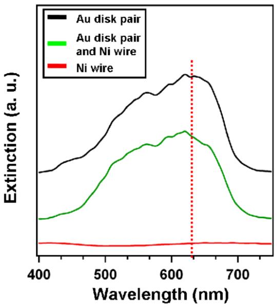
Dark field extinction spectra of an individual Au nanodisk pair (black), a Ni nanowire (red) and a multisegmented nanowire containing an Au nanodisk pair and a Ni nanowire (green). The red dotted line indicates the wavelength of the laser (632.8 nm) used to take the Raman spectra.
The above observations are confirmed with another Au-Ni multisegmented nanostructure that contains a 1.5 μm Au nanowire separated by 78 ± 8 nm from a 2.0 μm Ni nanowire (Figure S3). The weaker SERS intensity (compared to the Au nanodisk pair-Ni, Figure 1) is possibly due to poorer overlap between λmax of the Au nanowire and the incident wavelength (632.8 nm, red dotted line, Figure S3(c)).
Theoretical modeling strengthens our conclusions. The effect of the Au nanodisk pair on the SERS intensity associated with the nearby Ni nanowire can be inferred by comparing the ∣E∣4 enhancement on the Ni surface in Figures S4 (Ni nanowire 120 nm from an Au nanodisk pair) with the corresponding enhancement for a Ni nanowire in the absence of the Au nanodisk pair. Our calculations show that the ∣E∣4 enhancement factor (averaged over the surface) is a factor of 30 for the Au nanodisk pair-Ni structure in Figure S3 while it is only a factor of 10 for the Ni nanowire in the absence of the Au nanodisk pair. This demonstrates that the Au nanodisk pair produces significant enhancement in the SERS intensity (factor of ~ 3) associated with the nearby surface of the Ni nanowire. Thus, the direct transfer of excitation from the Au nanodisk pair to the Ni nanowire is what leads to the SERS enhancement in the experimental observation.
The observed long-range enhancement leads to a more comprehensive understanding of the SPR-enhanced EM fields with the distance from the nanostructure’s surface. SERS has been often thought of as having a range of a few nanometers from the nanostructures, as the previous studies were conducted by applying spacing materials between the Raman molecules and the surface of the nanomaterials.[19, 32] These spacing materials with higher dielectric constants (compared to air) lead to rapid decay of EM fields away from the nanostructures,[15] making it difficult to interrogate the relationship between the enhanced EM fields and the distance from the surface. In our approach, the probe molecules were separated from the SPR nanomaterials without high index spacing materials, which allows for the realization of much longer SERS distances (120 nm from the Au nanodisk pair).
These observations are fundamentally interesting and potentially technologically important. Traditionally, SPR-enhanced detection has been limited to the relatively few materials that have visible plasmon resonances and provide very large field enhancement (e.g. Au and Ag). Using this long range SERS, one can now consider strategies for probing reactions on SERS-inactive materials with adjacent noble metal nanostructures that are separated by distances that minimize quenching (in the case of fluorophores) but still allow for significant SPR-field enhancement.
Experimental Section
Multisegmented nanostructures were prepared via the OWL method.[20] In a typical experiment, 360 nm-diameter Au-Ag-Au-Ag-Ni nanowires were synthesized by template-directed electrochemical synthesis,[21-24] and then half-coated with a 50 nm thick silica (SiO2) layer by plasma-enhanced chemical vapor deposition (PECVD). After silica deposition, the sacrificial Ag segments were dissolved, which created gaps between the Au-Au and Au-Ni segments along the long axes of the nanowires. The Ag etching and silica coating were confirmed by SEM/EDX (Scanning Electron Microscope/Energy Dispersive X-Ray). In the OWL process, the length of each segment can be precisely controlled simply by controlling the charge (number of Coulombs) passed during electrochemical deposition. Segment number and composition also can be controlled so that it is easy to prepare wires with multiple gap, gaps of different lengths,[33] and segments of different compositions.
Phthalic acid (benzene-1,2-dicarboxylic acid) was selected as the Raman active molecule because the carboxyl group adsorbs onto Ni but not Au surfaces.[28, 34] To effectively modify the surface with phthalic acid, the nanowires were first isolated from an ethanol solution by centrifugation, and then resuspended in a 100 μL ethanol solution of phthalic acid (20 mM) and shaken for 24 hours. The phthalic acid-modified nanowires were subsequently isolated by centrifugation and repeatedly washed with ethanol to remove free and physisorbed phthalic acid, and then cast onto piranha-pretreated glass substrates.
Raman spectra and images were recorded with a confocal Raman microscope (Alpha WiTec Instruments) equipped with a piezo scanner and 100× microscope objective (NA = 0.90, Nikon, Tokyo, Japan).[27] The spatial resolution was 300 nm in this experiment. Samples were excited using a He-Ne laser (632.8 nm, Coherent Inc., Santa Clara, CA) with a spot size of ~ 1 μm and a power density of ~ 104 W/cm2 on the samples. For a typical Raman image with a scan range of 15 μm × 15 μm, complete Raman spectra were acquired on every pixel with an integration time of 0.3 s per spectrum and an image resolution of 100 pixels × 100 lines. To provide a careful analysis of the enhanced Raman scattering signal of phthalic acid on the sample features, all images presented here were processed by integrating the intensity of the Raman spectra at 1346 cm−1 (Figure S1), which is attributed to the νs(COO-) mode of the carboxylate group.[35] The microscopic length of the nanowire allows one to spectroscopically address and distinguish each set of nanostructures decorating the silica layer backing along the long wire axis independently. The experiments have been reproduced multiple times, with additional measurements on more OWL-fabricated multisegmented nanowires.
The dark field extinction spectra of single Au nanowire, single Au nanodisk pair, single Ni nanowire and Au-Ni multisegment nanowire were acquired using a Zeiss microscopy (Axiovert 100A) equipped with a CRAIC spectrometer (QDI301) and 100× microscope objective (NA = 0.90, Nikon, Tokyo, Japan). A halogen lamp (HAL 100) was used as the light source.
Supplementary Material
Acknowledgments
[**] C.A.M. acknowledges the Office of Naval Research (ONR) and the NSSEF program of the DoD for generous financial support. C.A.M is also grateful for a NIH Director’s Pioneer Award. G. C. S and S. L. thank the US Department of Energy under grant No. DEFG02-03-ER15487.
Footnotes
 Supporting information for this article is available on the WWW under http://www.angewandte.org or from the author.
References
- [1].Kreibig U, Vollmer M. Optical Properties of Metal Clusters. Springer-Verlag; Berlin, Germany: 1995. [Google Scholar]
- [2].Raether H. Surface Plasmons. Springer; New York: 1988. [Google Scholar]
- [3].Aizpurua J, Garnett WB, Lee JR, Abajo J. G. d., Brian KK, Mallouk T. Phys. Rev. B. 2005;71:235420. [Google Scholar]
- [4].Krenn JR. Nat. Mater. 2003;2:210. doi: 10.1038/nmat865. [DOI] [PubMed] [Google Scholar]
- [5].Moskovits M. Rev. Mod. Phys. 1985;57:783. [Google Scholar]
- [6].Geshev PI, Fischer UC, Fuchs H. Optics Express. 2007;15:13796. doi: 10.1364/oe.15.013796. [DOI] [PubMed] [Google Scholar]
- [7].Murphy CJ, Gole AM, Hunyadi SE, Stone JW, Sisco PN, Alkilany A, Kinard BE, Hankins P. Chem. Commun. 2008:544. doi: 10.1039/b711069c. [DOI] [PubMed] [Google Scholar]
- [8].Eustis S, El-Sayed M. J. Phys. Chem. B. 2005;109:16350. doi: 10.1021/jp052951a. [DOI] [PubMed] [Google Scholar]
- [9].Alivisatos P. Nat. Biotech. 2004;22:47. doi: 10.1038/nbt927. [DOI] [PubMed] [Google Scholar]
- [10].Jiang J, Bosnick K, Maillard M, Brus L. J. Phys. Chem. B. 2003;107:9964. [Google Scholar]
- [11].Cao YC, Jin R, Mirkin CA. Science. 2002;297:1536. doi: 10.1126/science.297.5586.1536. [DOI] [PubMed] [Google Scholar]
- [12].Keating CD, Kovaleski KM, Natan MJ. J. Phys. Chem. B. 1998;102:9404. [Google Scholar]
- [13].Nie SM, Emory SR. Science. 1997;275:1102. doi: 10.1126/science.275.5303.1102. [DOI] [PubMed] [Google Scholar]
- [14].Graham D, Faulds K. Chem. Soc. Rev. 2008;37:1042. doi: 10.1039/b707941a. [DOI] [PubMed] [Google Scholar]
- [15].Willets KA, Van Duyne RP. Annu. Rev. Phys. Chem. 2007;58:267. doi: 10.1146/annurev.physchem.58.032806.104607. [DOI] [PubMed] [Google Scholar]
- [16].Fang Y, Wei Y, Bai C, Kan L.-s. J. Phys. Chem. 1996;100:17410. [Google Scholar]
- [17].Tian Z-Q, Ren B, Li J-F, Yang Z-L. Chem. Commun. 2007:3514. doi: 10.1039/b616986d. [DOI] [PubMed] [Google Scholar]
- [18].Barbillon G, Bijeon JL, Bouillard JS, Plain J, De La Chapelle M. Lamy, Adam PM, Royer P. J. Microsc. 2008;229:270. doi: 10.1111/j.1365-2818.2008.01898.x. [DOI] [PubMed] [Google Scholar]
- [19].Dieringer JA, McFarland AD, Shah NC, Stuart DA, Whitney AV, Yonzon CR, Young MA, Zhang X, Van Duyne RP. Faraday Discuss. 2006;132:9. doi: 10.1039/b513431p. [DOI] [PubMed] [Google Scholar]
- [20].Qin L, Park S, Huang L, Mirkin CA. Science. 2005;309:113. doi: 10.1126/science.1112666. [DOI] [PubMed] [Google Scholar]
- [21].Possin GE. Rev. Sci. Instrum. 1970;41:772. [Google Scholar]
- [22].Preston CK, Moskovits M. J. Phys. Chem. 1993;97:8495. [Google Scholar]
- [23].Hurst SJ, Payne EK, Qin L, Mirkin CA. Angew. Chem. Int. Ed. 2006;45:2672. doi: 10.1002/anie.200504025. [DOI] [PubMed] [Google Scholar]
- [24].Martin CR. Science. 1994;266:1961. doi: 10.1126/science.266.5193.1961. [DOI] [PubMed] [Google Scholar]
- [25].Chen X, Jeon Y-M, Jang J-W, Qin L, Huo F, Wei W, Mirkin CA. J. Am. Chem. Soc. 2008;130:8166. doi: 10.1021/ja800338w. [DOI] [PMC free article] [PubMed] [Google Scholar]
- [26].Wei W, Li S, Qin L, Xue C, Millstone JE, Xu X, Schatz GC, Mirkin CA. Nano Lett. 2008;8:3446. doi: 10.1021/nl8023164. [DOI] [PMC free article] [PubMed] [Google Scholar]
- [27].Qin L, Zou S, Xue C, Atkinson A, Schatz GC, Mirkin CA. Proc. Natl. Acad. Sci. U.S.A. 2006;103:13300. doi: 10.1073/pnas.0605889103. [DOI] [PMC free article] [PubMed] [Google Scholar]
- [28].Sakata Y, Domen K, Maruya K, Onishi T. Catal. Lett. 1990;4:169. [Google Scholar]
- [29].Bauer LA, Reich DH, Meyer GJ. Langmuir. 2003;19:7043. [Google Scholar]
- [30].Salem AK, Searson PC, Leong KW. Nat. Mater. 2003;2:668. doi: 10.1038/nmat974. [DOI] [PubMed] [Google Scholar]
- [31].Ren B, Liu G-K, Lian X-B, Yang Z-L, Tian Z-Q. Anal. Bioanal. Chem. 2007;388:29. doi: 10.1007/s00216-007-1141-2. [DOI] [PubMed] [Google Scholar]
- [32].Whitney AV, Elam JW, Zou S, Zinovev AV, Stair PC, Schatz GC, Van Duyne RP. J. Phys. Chem. B. 2005;109:20522. doi: 10.1021/jp0540656. [DOI] [PubMed] [Google Scholar]
- [33].Martin CR, Baker LA. Science. 2005;309:67. doi: 10.1126/science.1114663. [DOI] [PubMed] [Google Scholar]
- [34].Salem AK, Searson PC, Leong KW. Nat. Mater. 2003;2:668. doi: 10.1038/nmat974. [DOI] [PubMed] [Google Scholar]
- [35].Tourw E, Baert K, Hubin A. Vib. Spectrosc. 2006;40:25. [Google Scholar]
Associated Data
This section collects any data citations, data availability statements, or supplementary materials included in this article.