Graphical abstract
Keywords: Porous silicon, Electrodeposition, Magnetic nanostructures, Ferromagnetism
Abstract
Electrodeposition of ferromagnetic metals, a common method to fabricate magnetic nanostructures, is used for the incorporation of Ni structures into the pores of porous silicon templates. The porous silicon is fabricated in various morphologies with average pore-diameters between 40 and 95 nm and concomitant pore-distances between 60 and 40 nm. The metal nanostructures are deposited with different geometries as spheres, ellipsoids or wires influenced by the deposition process parameters. Furthermore small Ni-particles with diameters between 3 and 6 nm can be deposited on the walls of the porous silicon template forming a metal tube. Analysis of this tube-like arrangement by transmission electron microscopy (TEM) shows that the distribution of the Ni-particles is quite narrow, which means that the distance between the particles is smaller than 10 nm. Such a close arrangement of the Ni-particles assures magnetic interactions between them. Due to their size these small Ni-particles are superparamagnetic but dipolar coupling between them results in a ferromagnetic behavior of the whole system. Thus a semiconducting/ferromagnetic hybrid material with a broad range of magnetic properties can be fabricated. Furthermore this composite is an interesting candidate for silicon based applications and the compatibility with today’s process technology.
1. Introduction
There is much interest in the fabrication of materials when their characteristic length scale comes into the nanometer range not only because of the miniaturized size but also because of the arising novel physical properties. The fabrication of nanostructures is often achieved by top-down or bottom-up processes in using lithographic methods but of special interest is also the self-assembly of nanostructures and nanoparticles on surfaces and in 3-dimensional arrays. Many works report on nanoparticles dispersed in a host material as another metal [1] or a nonmagnetic matrix [2]. In many cases polymers are utilized as matrix to investigate the properties of the composite as well as the interaction between the magnetic particles [3]. Silica is also used as host for the fabrication of a superparamagnetic composite material with particle-size dependent properties [4]. Metal nanostructures are often deposited within the pores of porous materials [5–7] to investigate the deposition process or for various applications. In the present work we report on the incorporation of various Ni nanostructures into the pores of porous silicon to achieve a magnetic/semiconducting composite. Porous silicon matrices with straight channels grown normal to the silicon surface are fabricated and within the pores ferromagnetic metal structures are electrochemically deposited. The shape and size of the deposits as well as the spatial distribution within the pores can be controlled by the electrochemical process parameters and thus samples with adjustable magnetic properties can be achieved. The combination of a semiconductor and a ferromagnetic material in one system brings together the electronic properties of silicon and the ferromagnetic behavior of the Ni nanostructures.
2. Experiments
For the formation of mesoporous silicon matrices highly n-doped silicon is used as substrate. The pore formation is carried out by anodization in an 8 wt% aqueous hydrofluoric acid solution. By varying the current density between 50 and 150 mA/cm2 matrices with pore-diameters between 35 and 100 nm can be fabricated. The anodization is performed under electrical breakdown conditions and thus illumination of the backside of the samples to generate carriers is not necessary. The pores are straight and separated from each other, whereas the main growth direction is the (1 0 0)-direction. The pore-arrangement is self-assembled and offers a four-fold symmetry under certain conditions. Such more or less regular structures are obtained by applying a constant current density between 75 and 100 mA/cm2 [8]. For higher current densities the critical current density JPS is reached and instead of pore formation electropolishing at the porous silicon/silicon border takes place [9], whereas in the case of lower current densities the pore-diameter becomes smaller and less regular. In the case of smaller pore-diameters (<35 nm) the distance between the pores becomes greater than twice the thickness of the space charge region which allows the nucleation of pores in these remaining silicon walls.
In a further electrochemical step within these pores a ferromagnetic metal as Ni is deposited resulting in a composite material consisting of a silicon matrix and precipitated Ni nanostructures. The deposition is performed in a pulsed way under cathodic conditions. As electrolyte an adequate metal salt solution is employed. In the case of Ni-deposition the so called Watts electrolyte (NiCl2, NiSO4) with boric acid as buffer is used. A variation of the pulse frequencies and the current density leads to modifications of the geometry and spatial distribution within the pores of the metal deposits [10]. Magnetic measurements are carried out by SQUID-magnetometry (SQUID magnetometer Cryogenics) up to a magnetic field of 6 T and in a temperature range between 4 and 250 K. The structure and composition of the nanocomposite is investigated by scanning electron microscopy (SEM) and transmission electron microscopy (TEM).
3. Discussion
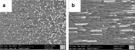
The magnetic/semiconducting composite which is fabricated in two electrochemical steps offers ferromagnetic properties depending on the process parameters. The morphology of the porous silicon matrices can be varied in pore-diameter, pore-distance and pore-length. A clear separation of the channels is important to assure that metal structures of neighboring pores are not connected. Thus the current density has to be adjusted that the distance between the pores does not exceed twice the thickness of the space charge region of the substrate which is around 10 nm for highly doped silicon. Dendritic growth of the pores always occurs in this morphology regime which means that small side-pores (length smaller than the pore-radius) grow in (1 1 1)-direction additionally to the main-pores [11]. The precipitation of the Ni structures within the pores takes also place by self-assembly resulting in a randomly arranged but more or less homogeneously over the entire porous matrix distributed metal nanostructure array. The cross-sectional images in Fig. 1 show the distribution of sphere-like and elongated Ni structures within the pores. The elongation of the Ni-structures is influenced by the pulse duration of the applied current. Spherical particles are precipitated in the case of a current density of 10 mA/cm2 and a pulse frequency of 0.025 Hz. Applying the same current density and increasing the pulse frequency to 0.2 Hz results in Ni wires with an elongation of a few micrometers.
Fig. 1.
(a) SEM-image (back scattered electrons) showing deposited Ni-particles with a maximum length of 100 nm and (b) precipitated Ni-structures with a maximum elongation of 1 μm within the pores.
Increasing the current density to 25 mA/cm2 and keeping the pulse frequency low small Ni particles of 3–6 nm in size are deposited on the pore walls. An enhancement of the current density leads to an increase of the packing density of the particles. Densely packed particles form a tube-like arrangement (Fig. 2). The thickness of the tube wall is around 5 nm and the diameter corresponds to the pore-diameter which is about 60 nm.
Fig. 2.

Ni-particles of 3–6 nm in size deposited in a tube-like arrangement around the pore wall. The thickness if the tube is about 5 nm and the tube diameter is about 60 nm.
The control of the geometry and distribution of the metal deposits by adjusting accurately the electrochemical parameters leads to a nanocomposite with tunable magnetic properties in a broad range. This range can be extended by choosing different materials or alloys.
In general the crystal orientation of the deposited metal structures, which is also one determining part of the magnetic behavior, can be determined from XRD but also from HRTEM-images [12]. In the case of Ni precipitated within the pores of porous silicon top view investigations give the information that different particles do not exhibit the same crystal orientation. In investigating the cross-section of the samples and considering an elongated single Ni-structure from preliminary measurements it can be assumed that the deposits are polycrystalline.
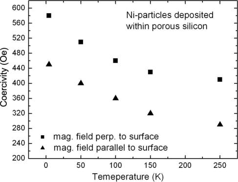
Considering the temperature dependence of the coercivity (HC) of porous silicon with precipitated Ni-particles (Fig. 3) and elongated Ni-structures (Fig. 4) one sees that HC is smaller for the elongated structures.
Fig. 3.
Temperature dependence of the coercivities of porous silicon with deposited Ni-particles (<100 nm) measured in two directions of magnetization with an applied field perpendicular (squares) and parallel (triangles) to the surface. The temperature is varied between 4 and 250 K.
Fig. 4.
Coercivities of samples with elongated Ni-structures (∼1 μm) deposited within the pores. HC decreases with increasing temperature. The coercivities are smaller if the magnetic field is applied parallel to the sample surface.
HC varies in the case of Ni-particles between 580 Oe (T = 4 K) and 410 Oe (T = 250 K), if the magnetic field is applied perpendicular to the sample surface meaning parallel to the pores. In the case of elongated structures HC decreases to values between 330 Oe (T = 4 K) and 200 Oe (T = 250 K). If the magnetic field is applied parallel to the sample surface a further decrease of the coercivity is always observed (Figs. 3 and 4) which are mainly caused by the shape-anisotropy of the precipitated metal-structures.
The different geometry of the embedded metal structures offers various anisotropic behavior. Particles which are deposited in a dense distribution (distance between the particles in the range of the particle size) seem to interact magnetically within the pores and thus samples show a higher anisotropy between the two magnetization directions than loosely packed particles. The value of the coercivity HC for a magnetic field applied parallel to the surface is about 23% less than for a field applied normal to the surface. In the case of elongated structures the anisotropy is similar (∼27%). The elongated structures are packed less densely than in the case of particles but the anisotropy is caused by the shape. In the case of closely packed particles they seem to form a magnetic quasi chain resulting in a shape anisotropy. An estimation of the theoretical values of elongated Ni-structures with an aspect ratio of about 20 is in good agreement with the literature [13]. It is assumed that particles which are deposited with a distance much greater than their size offer a weak dipolar coupling and therefore no significant magnetic anisotropy can be observed (Fig. 5).
Fig. 5.
(a) Magnetization of a specimen with Ni-particles with a distance much greater than their size, measured at T = 4 K with a magnetic field applied perpendicular (full line) and parallel (dotted line) to the surface, respectively. There is no significant anisotropy, the coercivities are nearly equal (HC = 800 Oe). (b) Cross-sectional SEM-image showing the spare distribution of the Ni-particles.
Concerning the magnetic anisotropy the crystal orientation of the deposited Ni-particles is also of interest because different crystalline phases offer various magnetocrystalline anisotropies [12,14]. In the case of elongated structures the shape plays a dominant role which determines the magnetic anisotropy.
Considering the anisotropy between easy axis (magnetic field perpendicular to the surface) and hard axis (magnetic field parallel to the surface) magnetization the differences of the coercivities are for any morphology in the same range for the whole temperature regime (between 4 and 250 K) which can be seen in Figs. 3 and 4.
Magnetic remanence MR versus temperature for samples containing mainly Ni-particles and such with a high amount of precipitated Ni-wires is shown in Fig. 6. In both cases the remanence decreases with increasing temperature.
Fig. 6.
Temperature dependent magnetic remanence MR for porous silicon containing Ni-particles (a) and Ni-wires (b). The measurements have been performed with a magnetic fields applied perpendicular and parallel to the sample surface.
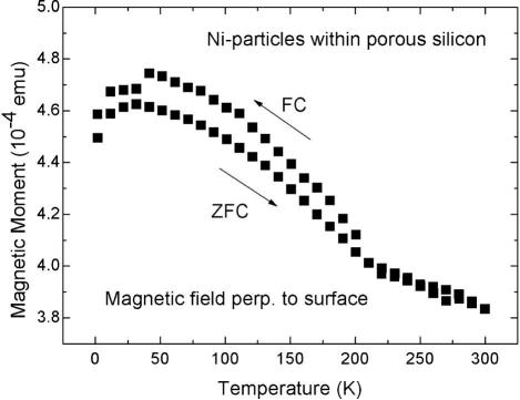
The blocking temperature of the various systems can be determined from zero field cooled (ZFC)/field cooled (FC) measurements. Temperature dependent measurements of samples containing mainly Ni-wires do not offer a distinct peak, which in general indicates the blocking temperature TB but a monotonically increasing curve with increasing temperature (ZFC-branch) and a slightly increasing FC-branch with decreasing temperature [15]. Both indicates that the deposits of this system strongly dipolar interact. Furthermore such flat curves indicate demagnetizing effects. The splitting of the two branches is around 325 K, whereas the highest values of the ZFC-branch are around 300 K which results in a TB in the range of the room temperature or above (Fig. 7a). In the case of deposited Ni-particles the blocked state should be more distinct but due to a broad particle size distribution which is known from TEM images the peak is quite broad and TB influenced by dipolar coupling offers a value of about 50 K (Fig. 7b).
Fig. 7a.
Temperature dependent magnetization measurements (T between 4 and 350 K) of a porous silicon/Ni composite containing mainly elongated Ni-structures. Strong coupling and demagnetizing effects of the wire-like structures are responsible for the flat shape of the ZFC/FC curves.
Fig. 7b.
ZFC/FC measurements of porous silicon with deposited Ni-particles performed between T = 4 K and T = 300 K. The broad peak is due to a broad particle size distribution (known from TEM-images). The blocking temperature around 50 K indicates dipolar coupling between the particles.
In the case of Ni-tubes covering the pore walls the magnetic behavior is comparable with the one of wire-like structures. The difference of the coercivities between the two magnetization directions is also around 30%.
All in all one can say that the presented semiconductor/metal system offers ferromagnetic properties which can be tuned by the deposition parameters by varying e.g. the puls-frequency, current density and electrolyte concentration. The temperature of the electrolyte during deposition is also an important factor but it has been kept constant at room temperature during the presented experiments.
4. Conclusions
A nanocomposite system consisting of a semiconducting matrix and embedded ferromagnetic nanostructures has been fabricated. The ferromagnetic characteristics as coercivity, remanence and magnetic anisotropy of the nanocomposite can be adjusted by the electrochemical parameters. Furthermore the spatial distribution of the metal structures within the pores can be varied which means that the magnetic interactions between the particles can be influenced. In the case of densely packed particles within the pores dipolar coupling between them occurs and results in quasi magnetic chains which offer a much larger magnetic anisotropy than non-interacting particles. By modifying the current density small Ni-particles (3–6 nm) can be deposited. If the packing density of these particles is sufficiently close, Ni-tubes of a few nanometer in thickness are covering the pore walls. The presented nanocomposite is an interesting system for magnetic applications as magnetic sensor technology. Silicon as substrate renders this composite a good candidate for the integration in existing process technology.
Acknowledgements
This work is supported by the Austrian science Fund FWF under Project P21155. The authors thank M. Dienstleder from the Institute for Electron Microscopy at the University of Technology Graz, Austria for sample preparation by focused ion beam.
References
- 1.Nordblad P. J. Phys. D Appl. Phys. 2008;41:134011. [Google Scholar]
- 2.Bräuer B., Vaynzof Y., Zhao W., Kahn A., Li W., Zahn D.R.T., Fernandez C. de J., Sangregorio C., Salvan G. J. Phys. Chem. B. 2009;113:4565. doi: 10.1021/jp809777z. [DOI] [PubMed] [Google Scholar]
- 3.Guskos N., Typek J., Bodziony T., Roslaniec Z., Narkiewicz U., Kwiatkowska M., Maryniak M. Rev. Adv. Mater. Sci. 2006;12:133. [Google Scholar]
- 4.Montemayor S.M., Garcia-Cerda L.A., Torres-Lubian J.R., Rodriguez-Fernandez O.S. Mater. Res. Bull. 2008;43:1112. [Google Scholar]
- 5.Li W., Shen T.H. Microelectron. Eng. 2007;84:1436. [Google Scholar]
- 6.Fukami K., Kobayashi K., Matsumoto T., Kawamura Y.L., Sakka T., Ogata Y.H. J. Electrochem. Soc. 2008;155:D443–D448. [Google Scholar]
- 7.Fang Ch., Foca E., Xu S., Carstensen J., Föll H. J. Electrochem. Soc. 2007;154:D45–D49. [Google Scholar]
- 8.Granitzer P., Rumpf K., Poelt P., Albu M., Chernev B. Phys. Status Solidi C. 2009;6:2222. [Google Scholar]
- 9.Lehmann V. J. Electrochem. Soc. 1993;140:2836. [Google Scholar]
- 10.Rumpf K., Granitzer P., Pölt P. Nanoscale Res. Lett. 2010;5:379. doi: 10.1007/s11671-009-9492-6. [DOI] [PMC free article] [PubMed] [Google Scholar]
- 11.Lehmann V., Rönnebeck S. J. Electrochem. Soc. 1999;164:2968. [Google Scholar]
- 12.Chen Y., Peng D.-L., Lin D., Luo X. Nanotechnology. 2007;18:505703. [Google Scholar]
- 13.Skomski R. J. Phys. Condens. Matter. 2003;15:R841. [Google Scholar]
- 14.Cheng J., Zhang X., Ye Y. J. Solid State Chem. 2006;179:91. [Google Scholar]
- 15.Zhang P., Zuo F., Urban F.K., Khabari A., Griffiths P., Hosseini-Tehrani A. J. Magn. Magn. Mater. 2001;225:337. [Google Scholar]


