Abstract
ZnO nanorod arrays are prepared on a silicon wafer through a multi-step hydrothermal process. The aspect ratios and densities of the ZnO nanorod arrays are controlled by adjusting the reaction times and concentrations of solution. The investigation of field emission properties of ZnO nanorod arrays revealed a strong dependency on the aspect ratio and their density. The aspect ratio and spacing of ZnO nanorod arrays are 39 and 167 nm (sample C), respectively, to exhibit the best field emission properties. The turn-on field and threshold field of the nanorod arrays are 3.83 V/μm and 5.65 V/μm, respectively. Importantly, the sample C shows a highest enhancement of factorβ, which is 2612. The result shows that an optimum density and aspect ratio of ZnO nanorod arrays have high efficiency of field emission.
Keywords: ZnO nanorod, Arrays, Field emission, Aspect ratio, Density
Introduction
ZnO is an important functional II–VI semiconductor compounds and have been extensively investigated for their excellent optoelectronic, electronic, photochemical properties [1,2]. Various methods including chemical, electro-chemical, and physical deposition techniques have been employed to synthesize 1D ZnO nanostructures [3-5]. On the other hand, the wet-chemical methods [6-8] have been used for producing varied ZnO one-dimensional (1D) nanostructures, such as nanotube [9], nanopencil [10], nanoneedle [11], and nanoscrew [12]. Recent experiments have shown that the ZnO 1D nanostructures have excellent field emission properties, far better than other semiconductors [10,11,13,14]. An important advantage of using aligned nanorods, nanowires, nanobelts, and nanotubes for field emission is their high aspect ratio. The field enhancement factor β is a key parameter which is determined by turn-on field, threshold field, and work function. Also, the value of β relates to the structure, shape, size, alignment, crystalline, aspect ratio, etc. [15]. Many effects, such as morphological effects [16], surface states [17], and densities of nanorods [18] have been studied. Zhao et al. [16] investigated the morphological effects on the field emission of ZnO nanorod arrays. The result showed that the ZnO nanoneedle arrays exhibit excellent properties due to their small emitter radius and high nanorod density remarkably reduces the local field at the emitters owing to the screening effect. Wang et al. [18] investigated the density effects on the field emission of ZnO nanorods and pointed out that the mezzo density of ZnO nanorods had the best field emission properties. But there is no report about the aspect ratio effects on the field emission properties of ZnO nanorod arrays. In this work, ZnO nanrod arrays with different aspect ratios and densities are synthesized by controlling the reaction times and concentrations of solution. The field emission properties of ZnO nanorod arrays with different aspect ratios and densities have been investigated for showing the enhancement factor β was enhanced with increasing the aspect ratio of ZnO nanorods and the enhancement factor β was decreased with reducing the density of nanorods. An optimum density and aspect ratio of ZnO nanorod arrays (sample C) have high efficiency of field emission. A model has been used for the explanation of the results.
Experimental Details
The ZnO nanorod arrays were prepared on a silicon wafer (4 × 5 cm2) through a multi-step hydrothermal process [6]. Firstly ZnO nanocrystals colloid (4 × 10⁻³ M) is spin-coated 15 times on the silicon wafer at the speed of 3000 r/s to form a thick film of ZnO nanocrystals and ZnO nanocrystlas film annealed at 400 °C for 2 h under atmosphere. Then the silicon wafer is immersed into the aqueous solution (250 mL) of 0.04 M zinc nitrate hexahydrate/hexamethylenetetramine at 75 °C. After keeping it for 10 h in this solution, the surface of silicon wafer is coated for forming a layer of white film, which is washed by deionized water three times, and dried in air at room temperature. A piece of the silicon wafer (1 × 4 cm2) is cut as sample A. The remnant wafer (4 × 4 cm2) is reinserted into the aqueous solution (250 mL) of 0.04 M zinc nitrate hexahydrate/hexamethylenetetramine at 75 °C for 10 h and the sample B is obtained by cutting a piece from the above mentioned silicon wafer (1 × 4 cm2). The nanorods are able to form bundles if the sample B is immersed into 0.04 M aqueous solution of zinc nitrate hexahydrate/hexamethylenetetramine at 75 °C for 10 h. The concentration of reaction solution is reduced to 0.03 M and a remnant wafer (3 × 4 cm2) is kept into the aqueous solution (250 mL) of 0.03 M of zinc nitrate hexahydrate/hexamethylenetetramine at 75 °C for 10 h and the sample C (1 × 4 cm2) is obtained from the above method. Samples D and E are obtained by repeating the reaction process several times.
The arrays of ZnO nanorods are characterized and analyzed by field emission scanning electron microscopy (FESEM) and X-ray diffraction (XRD). The SEM images are obtained with a JEOL JSM 6700F field emission scanning electron microscope. The XRD patterns are recorded with a Japan Rigaku D/max-2500 rotation anode X-ray diffractometer equipped with graphite-monochromatized Cu Kα radiation (λ = 1.54178 Å), employing a scanning rate of 0.05°s−1in the 2θ range from 20° to 60°.
The field emission properties of ZnO nanorod arrays are measured using a two-parallel-plate configuration in a homemade vacuum chamber at a base pressure of ~1.0 × 10⁻⁶ Pa at room temperature. The sample is attached to one of the stainless-steel plates which is cathode with the other plate as anode. The distance between the electrodes is 300 μm. A direct current voltage sweeping from 0 to 5000 V was applied to the sample at a step of 50 V. The emission current is monitored using a Keithley 6485 picoammeter.
Results and Discussion
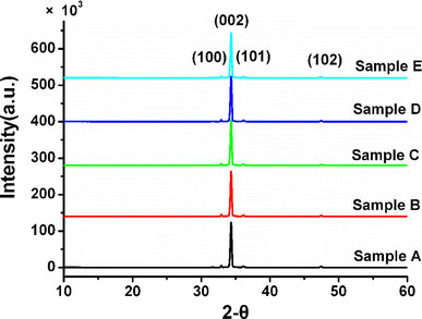
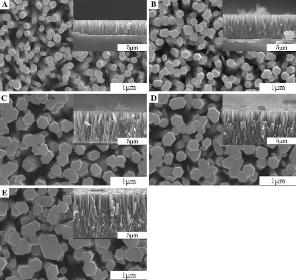
The XRD patterns of those ZnO nanorod arrays are shown in Fig. 1. The diffraction peaks are identified to match the hexagonal ZnO crystalline with wurtzite structure and preferentially aligned in the c-axis direction [0001]. As shown in Fig. 2, for the samples A, B, C, D, and E, the ZnO nanorod arrays aligned on the silicon wafers. The average radiuses of samples A, B, C, D, and E are 90 ± 2 nm, 125 ± 5 nm, 136 ± 5 nm, 150 ± 5 nm, and 168 ± 5 nm, respectively. The average lengths of samples A, B, C, D, and E are 2.5 ± 0.05 μm, 4.2 ± 0.05 μm, 5.3 ± 0.05 μm, 6.3 ± 0.1 μm, and 7.4 ± 0.1 μm, respectively. From sample A to sample B the average radiuses and lengths of ZnO nanorods obviously increased about to 35 nm and 1.7 μm when the reaction times are increased. From sample B to sample E, the average radiuses and lengths of ZnO nanorods equably increased by ~15 nm and ~1 μm. The radiuses and lengths of ZnO are able to be accurately controlled by adjusting the concentration of reactants and reaction times. The average spacing of nanorods of samples A, B, C, D, and E are 195 ± 10 nm, 183 ± 10 nm, 167 ± 10 nm, 143 ± 10 nm, and 126 ± 10 nm, respectively. The average radiuses, lengths, and spacing of the nanorods are listed in Table 1. The aspect ratios of the samples A, B, C, D, and E are 28, 34, 39, 42, and 44, respectively.
Figure 1.

XRD patterns of those ZnO nanorod arrays
Figure 2.

The SEM images of samples A, B, C, D, and E. The inset images are the section view of samples
Table 1.
The morphological characteristic and field emission property of ZnO nanorod arrays. (r: the average radius;L: the length of nanorod;β: the field enhance factor;s: the spacing of nanorods)
| Sample | r(nm) | L(μm) | L/r | s(nm) | Turn-on field (V/μm) | Threshold field (V/μm) | β |
|---|---|---|---|---|---|---|---|
| A |
90 ± 2 |
2.5 ± 0.05 |
28 |
195 ± 10 |
6.33 |
8.58 |
1103 |
| B |
125 ± 5 |
4.2 ± 0.05 |
34 |
183 ± 10 |
5.16 |
7.43 |
1772 |
| C |
136 ± 5 |
5.3 ± 0.05 |
39 |
167 ± 10 |
3.83 |
5.65 |
2612 |
| D |
150 ± 5 |
6.3 ± 0.1 |
42 |
143 ± 10 |
4.16 |
6.57 |
2382 |
| E | 168 ± 5 | 7.4 ± 0.1 | 44 | 126 ± 10 | 4.65 | 6.97 | 1760 |
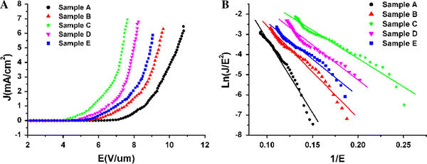
The current density–electric field (J–E) curves and the corresponding Fowler-Nordheim (F-N) plots of ZnO nanorod arrays are illustrated in Fig. 3a and b, respectively. The important field emission parameters extracted from these current density–electric field (J–E) curves are listed in Table 1. Here we define the turn-on field (Eto) and the threshold field (Eth) as the applied electric fields required to produce a current of 10 μA/cm2and 1 mA/cm2, respectively. The Etoof samples A, B, C, D, and E are 6.33 V/μm, 5.16 V/μm, 3.83 V/μm, 4.16 V/μm and 4.65 V/μm, respectively. The Ethof sample A, B, C, D and E are 8.58 V/μm, 7.43 V/μm, 5.65 V/μm, 6.57 V/μm, and 6.97 V/μm, respectively. The sample C has the lowest turn-on field (3.83 V/μm) and threshold field (5.65 V/μm), which indicates that the sample C has the best field emission properties in these samples.
Figure 3.

The field emission properties of ZnO nanorod arrays: (a) J–E plots. (b) The corresponding F-N plots
To further analyze the field emission properties of the ZnO nanorod arrays, the class Fowler-Nordheim (F-N) law [19], which was induced on the basis of the electron emission properties from a semi-infinite flat metallic surface, was used to describe the relationship between the J and the local field nearby the emitter.  is usually related to the average applied field E as follows:
  where d is the inter-electrode spacing, V is the applied voltage, and β is the enhance factor. The F-N law is expressed as
  where
where  ,
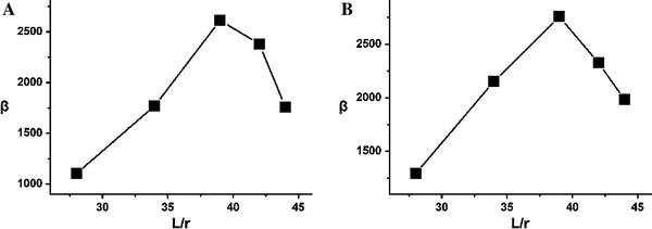
,  , and φ is the work function, which is estimated as 5.2 eV for ZnO [18]. The enhance factor β can be determined by fitting the slope value and taking a reasonable φ value. For those ZnO nanorod arrays, the F-N plots (Fig. 3b) show a rough linear relationship, implying that a quantum-tunneling mechanism is responsible for the emission. The obtained field enhancement factors from the F-N plots are summarized in Table 1. The field enhancement factors of samples A, B, C, D, and E are 1103, 1772, 2612, 2382, and 1760, respectively. The relationship of β and L/r is shown in Fig. 4a. The interesting result is that β is not linearly increasing with the aspect ratio. The apparent reasons might be due to the screening effect [20-25]. An empirical model [21] can be used to explain this phenomenon.
| (1) |
| (2) |
Figure 4.

The relationship between β and L/r. (a) The experiment results, (b) The simulation results
L and r are the length and the radius of ZnO nanorods. h is an alterable parameter which can be adjusted to fit the experiment data. β0 is the intrinsic field enhancement factor for a single emitter which is determined by the aspect ratio [21]. β is the field enhancement factor of the emitter array, which can be determined by the aspect ratio and the interspacing of nanorods (density effect). s is the interspacing of nanorods. When the aspect ratio increases gradually, β0 will keep up with it. Then the β will also increase gradually. When the interspacing s decreasing, there exists a negative effect on the increment of β. When s ≪ L, Eq. 2 has an approximate expression:
| (3) |
Where, C is alterable parameter. The alterable parameter h is chosen −26 to fit the data of samples A and B. Then using the formula (3), the stimulant relationship of β and L/r can be shown in Fig. 4b which shows the sample C (β = 2885) has the highest field enhancement factor. This simulation value is only slightly bigger than the actual value. In this case, β is not only related to aspect ratio but also dependent on s. For the low-density, the interspacing is large, and the screening effect is weak resulting in the field enhancement factor β increasing with the increase of aspect ratio. For the small interspacing, the screening effect is able to be domain factor leading to decrease in the field enhancement factor. These two opposite effects take place simultaneously; the enhancement factor shows a maximum value at balance point (aspect ratio: 38.9, interspacing: 178 nm), which is consistent with the sample C (aspect ratio: 39, interspacing: 167 ± 10 nm), for producing an optimization of field emission properties.
Conclusions
The arrays of ZnO nanorod with different aspect ratios and densities are constructed using a multi-step hydrothermal process by controlling the reaction times and concentrations. The field emission properties of ZnO nanorod arrays are investigated. The results show that the aspect ratio and the density of nanorod arrays play key roles in the field emission. The sample C exhibits the best field emission properties in these samples. The field enhancement factorβenhances with increasing the aspect ratio of the nanorod. For the small interspacing (s), the screening effect may become the domain factor which will decrease the field enhancement factorβ. When the interspacing (s) is larger than 167 nm, the enhancement factorβincreases with aspect ratio, linearly, while the screening effect can be negligible. But when thesis smaller than 167 nm, the screening effect becomes the domain factor. There exists a balance point (aspect ratio: 38.9, interspacing: 178 nm), in which the optimization field emission can be obtained.
Contributor Information
Huibiao Liu, Email: liuhb@iccas.ac.cn.
Yinglin Song, Email: ylsong@hit.edu.cn.
Acknowledgment
This work was supported by the National Nature Science Foundation of China (20531060, 20473102, and 20571078) and the National Basic Research 973 Program of China (Grant No. 2006CB932100 and 2005CB623602).
References
- Huang MH, Mao S, Feick H, Yan HQ, Wu YY, Kind H, Science. 1995. p. 61. [DOI] [PubMed]
- He H, Lao CS, Chen LJ, Davidovic D, Wang ZL. J. 2005. p. 16376. COI number [1:CAS:528:DC%2BD2MXhtFKlurzL] [DOI] [PubMed]
- Wu Y, Yang P. J. 2001. p. 3156.
- Chiou WT, Wu WY, Ting JM. Diam. 2003. p. 18411. [DOI]
- Park W, Yi G, Kim M, Pennycook SJ. Adv. 2002. p. 1841. COI number [1:CAS:528:DC%2BD3sXitlOitw%3D%3D] [DOI]
- Greene LE, Law M, Goldberger J, Kim F, Johnson JC, Zhang YF, Angew. 2003. p. 3031. COI number [1:CAS:528:DC%2BD3sXlslGksbw%3D] [DOI] [PubMed]
- Vayssieres L, Keis K, Hagfeldt A, Lindquist S-E. Chem. 2001. p. 4396.
- Yu HD, Zhang ZP, Han MY, Hao XT, Zhu FR. J. 2005. p. 2378. COI number [1:CAS:528:DC%2BD2MXovFSqsQ%3D%3D] [DOI] [PubMed]
- Wei A, Sun XW, Dong ZL, Yu MB, Huang W. Appl. 2006. p. 213012.
- Wang RC, Liu CP, Huang JL, Chen S-J, Tseng Y-K, Kung S-C. Appl. 2005. p. 013110. [DOI]
- Li YB, Bando Y, Golberg D. Appl. 2004. p. 3604.
- Liao L, Li JC, Liu DH, Wang DF, Song WZ. Appl. 2005. p. 083106. [DOI]
- Yang YH, Wang B, Xu NS, Yang GW. Appl. 2006. p. 043107. [DOI]
- Cao BQ, Cai WP, Duan GT, Li Y, Zhao Q, Yu DP. Nanotechnology. 2005. p. 2567. COI number [1:CAS:528:DC%2BD2MXhtlelsrfE] [DOI]
- Lee CJ, Lee TJ, Lyu SC, Zhang Y, Ruh H, Lee HJ. Appl. 2002. p. 3648. COI number [1:CAS:528:DC%2BD38XosVeisrw%3D] [DOI]
- Zhao Q, Zhang HZ, Zhu YW, Feng SQ, Sun XC, Xu J, Appl. 2005. p. 203115. [DOI]
- Zhao Q, Xu XY, Song XF, Zheng XZ, Yu DP. Appl. 2006. p. 033102. [DOI]
- Wang XD, Zhou J, Lao CS, Song JH, Xu NS, Wang ZL. Adv. 2007. p. 1627. COI number [1:CAS:528:DC%2BD2sXnsVagsb0%3D] [DOI]
- Fowler RH, Nirdheim LW. Proc. R. Soc. Lond. A. 1928. p. 173. COI number [1:CAS:528:DyaB1cXjt1Kktg%3D%3D] [DOI]
- Jo SH, Tu Y, Huang ZP, Carnahan DL, Wang DZ, Ren ZF. Appl. 2003. p. 3520. COI number [1:CAS:528:DC%2BD3sXjvVSls7c%3D] [DOI]
- Patra SK, Mohan Rao G. J. 2006. p. 024319. [DOI]
- Nilsson L, Growning O, Emmengegger C, Kyettek O, Schaller E, Schlaphach L, Appl. 2000. p. 2071. COI number [1:CAS:528:DC%2BD3cXitlSrsr0%3D] [DOI]
- Bonard J-M, Weiss N, Kind H, Kern K. Adv. 2001. p. 184. COI number [1:CAS:528:DC%2BD3MXhs12qu74%3D] [DOI]
- Chhowalla M, Ducati C, Rupesinghe NL, Teo KBK, Amaratunga GAJ. Appl. 2001. p. 2079. COI number [1:CAS:528:DC%2BD3MXntVWhs78%3D] [DOI]
- Suh JS, Jeong KS, Lee JS, Han I. Appl. 2002. p. 2392. COI number [1:CAS:528:DC%2BD38XisVersLw%3D] [DOI]


