Abstract
Multi-walled carbon nanotubes (MWNT) have been synthesized by chemical vapour decomposition (CVD) of acetylene over Rare Earth (RE) based AB2(DyNi2) alloy hydride catalyst. The as-grown carbon nanotubes were purified by acid and heat treatments and characterized using powder X-ray diffraction, Scanning Electron Microscopy, Transmission Electron Microscopy, Thermo Gravimetric Analysis and Raman Spectroscopy. Fully carbon based field emitters have been fabricated by spin coating a solutions of both as-grown and purified MWNT and dichloro ethane (DCE) over carbon paper with and without graphitized layer. The use of graphitized carbon paper as substrate opens several new possibilities for carbon nanotube (CNT) field emitters, as the presence of the graphitic layer provides strong adhesion between the nanotubes and carbon paper and reduces contact resistance. The field emission characteristics have been studied using an indigenously fabricated set up and the results are discussed. CNT field emitter prepared by spin coating of the purified MWNT–DCE solution over graphitized carbon paper shows excellent emission properties with a fairly stable emission current over a period of 4 h. Analysis of the field emission characteristics based on the Fowler–Nordheim (FN) theory reveals current saturation effects at high applied fields for all the samples.
Keywords: Multi-walled carbon nanotubes, DyNi2alloy hydride, Spin coating, Dichloro ethane, Graphitized carbon paper, CNT field emitter, Fowler–Nordheim theory
Introduction
Carbon nanotubes (CNTs) have been considered as one of the best candidates for field emission due to their unique properties such as high aspect ratio, chemical inertness, high mechanical strength and high electrical conductivity [1,2]. In spite of such excellent characteristics, the realization of CNT based vacuum microelectronics has been limited due to the absence of a stable film fabrication process over a suitable substrate. The mechanism of field induced electron emission from a nanotube is understood to be due to the applied electric field undergoing an increase at the tip of the CNT, which is often referred to as the field enhancement factor (β). The value of β depends on the length, radius and type of the structure [1,3,4]. Both single walled nanotubes (SWNT) and multi walled nanotubes (MWNT) have been reported as excellent field emitters at low operating voltages [1-5]. Carbon nanotubes are usually prepared by arc evaporation [6], laser ablation [7] or metal catalyzed CVD [8]. Catalysts with large surface area having active catalytic centers are vital for the large scale production of carbon nanotubes using CVD [9].
CNT based field emitters have been fabricated using different methods such as direct growth [10], screen printing [11], suspension filtering [12], electrophoresis [13] and spray method [14,15]. The major disadvantage with screen printing method is that one cannot study the intrinsic field emission nature of the CNTs due to the surface modification of nanotubes. Moreover, there will be substantial degradation of emission tips, which cannot be avoided [11]. In all other methods weak adhesion of CNTs to the substrate is a serious draw back, which often leads to catastrophic vacuum breakdown or arcing during device operation [16,17]. In addition, the electronic resistance between the CNTs and the substrate results in joule heating of the interface. This damages the electrical contact between the emitters and the substrate, there by increasing the voltage required for emission over extended periods [17,18].
In order to overcome such undesirable effects, we have fabricated a fully carbon based field emitter by spin coating a solution of MWNT over graphitized carbon paper. In this paper we report the fabrication of both as-grown and purified MWNT based field emitters by spin coating method over carbon paper with and without a graphitized layer. The purpose of this paper is to find out how the field emission properties are influenced by the purity of the MWNT and by the presence of the graphitic layer between the MWNT and the substrate (carbon paper). The field emission properties have been studied and the results have been discussed. The results show that this method opens several new possibilities for field emission devices.
Experimental
MWNT were synthesized by the decomposition of acetylene over RE based AB2(DyNi2) alloy hydride powders using a fixed- bed catalytic reactor as discussed in previous work [19]. The as-prepared MWNT were purified by air oxidation followed by acid treatment [19,20]. The samples were heated in air at 400 °C for 3 h to remove the amorphous carbon, lead to expose the catalytic metal surface. The catalytic impurities were then removed by refluxing with concentrated HNO3 for 24 h, followed by washing with de-ionized water and then the sample was dried in air for 30 min at 100 °C. The crystallinity and purity of the samples were verified by XRD (Cu-Kαradiation) and thermo gravimetric measurements (20 °C/min). The samples were characterized using Raman spectroscopy, SEM and TEM.
The graphitized carbon paper is a double layer structured gas diffusion layer porous carbon paper which consists of a macroporous layer of carbon fiber paper (SGL, Germany) and a microporous layer of carbon black powder and a hydrophobic agent. The carbon black powder enhances an intimate electronic contact between the CNTs and the macroporous carbon paper. The graphitized carbon paper was prepared by deposition of a mixture of carbon black and poly-tetrafluoroethylene powders onto carbon paper in combination with a subsequent rolling process.
For the fabrication of field emission arrays of randomly oriented as-grown MWNT over carbon paper, as-grown MWNT were first dispersed in 1, 2 dichloroethane (DCE). DCE helps the dispersion of MWNT without surface modification, besides being volatile [14,15]. The dispersion process involved the ultrasonication of 50 mg of MWNT in 10 ml of DCE for 1 h, followed by centrifugation at a speed of 5,000 rpm for 30 min to precipitate the undissolved MWNT. After decanting the supernatants, the as-grown MWNT-DCE solution was spin coated on the graphitized carbon paper at a speed of 3,200 rpm at room temperature to obtain a uniform distribution of randomly oriented MWNT on the graphitized carbon paper (Sample A). Sample B was prepared by spin coating of the as-grown MWNT-DCE solution over the carbon paper without the graphitized layer. Using the same method, purified MWNT were also spin coated over the graphitized carbon paper, to obtain field emission arrays of randomly oriented purified MWNT (Sample C). Sample D was prepared by spin coating of the purified MWNT-DCE solution over the carbon paper with out the graphitized layer.
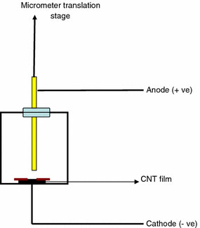
The field emission characteristics were studied using an indigenously fabricated set-up (Fig. 1). It consists of a cylindrical gold coated copper anode of 1 cm diameter and a stainless steel (SS) cathode. The carbon films were kept placed over the cathode and electrical contacts were made using silver paste. A dielectric spacer with a hole of 1 mm diameter was kept over the film. The whole arrangement was kept inside a vacuum chamber and all measurements were carried out at a base pressure of 2 × 10⁻⁶ torr. The distance between the emitting surface and the anode could be adjusted using a micrometer controlled translational stage and in the case of samples A and B the distance was held at 400 μm and for samples B and D, the separation was 500 μm. A DC power source was used for sourcing the voltage up to 2,000 V and current was measured with nA sensitivity.
Figure 1.

Schematic diagram of the field emission set up housed inside the vacuum chamber
Results and Discussion
The powder X-ray diffraction (XRD) patterns were obtained using an X’pert PRO, PANalytical diffractometer with nickel-filtered Cu Kα radiation under ambient air and scanning in the 2θ range of 10−90°, in steps of 0.05°. X-ray diffraction pattern of DyNi2 alloy shows the formation of single phase with a C 15 type cubic structure. XRD pattern of as-prepared CNTs using DyNi2alloy hydride catalyst shows the presence of the catalytic impurities, while the removal of these impurities can be verified from the XRD pattern of for purified CNTs. These results have been explained in detail in our previous work [21].
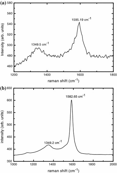
FT-Raman Spectroscopy studies were carried out on as-grown and purified MWNT, using WiTec GmbH confocal Raman microscope using argon ion laser having an excitation wavelength of 514.5 nm. Fig. 2a shows the Raman spectra of as-grown MWNT and Fig. 2b represents that of purified MWNT. Even though, similar peaks are observed in both the spectra, the spectral peaks are sharper in the case of purified MWNT. Its spectrum consists of two peaks at 1,595.16 cm−1 and 1,345.2 cm−1, which are designated as the tangential modes of CNTs. The peak at 1,595.16 cm−1 is due to the Raman-active E2g mode analogous to that of graphite, while that at 1345.2 cm−1 corresponds to that of disordered carbon.
Figure 2.

(a) Raman spectrum of as-grown MWNT, (b) Raman spectrum of purified MWNT
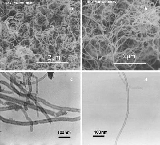
Figure 3a and b show respectively the SEM images (SEM; JEOL JSM 840 A) of as-grown and purified CNTs obtained by the catalytic decomposition of acetylene over hydrogen storage RE based AB2 alloy hydride catalyst. From the SEM image, it is evident that the packing density of carbon nanotubes is very high. As the bottom layer of the deposits inside the quartz tube were left out, not many of the catalytic particles were seen in the SEM image, unlike those reported by Gao et al. [22]. TEM images (Philips Electron Microscope, acceleration voltage 120 KV) of as-grown and purified MWNT are shown in Fig. 3c and d, respectively. The TEM micrograph shows that the nanotubes have an outer diameter of about 30 nm and an inner diameter of about 10 nm.
Figure 3.

(a) SEM image of the as-grown MWNT, (b) SEM image of the purified MWNT, (c) TEM image of the as-grown MWNT, (d) TEM image of the purified MWNT
The as-grown and purified samples were analyzed for their total carbon content by thermogravimetry in air (20 °C min−1) employing a Perkin-Elmer TGA 7 analyzer. A slight weight loss is observed below 500 °C for the purified sample which is due to the burning of amorphous carbon. Weight loss between 500°C and 700°C is assigned to the burning of MWNT. Final residual weight of 1.5% was obtained for the purified MWNT. The purity of the purified sample is about 95% whereas the TG curve for the as-grown MWNT indicates a purity of only 21%. The yield of MWNT is defined as the ratio of weight loss between 500 °C and 700 °C to the weight that remain at 850 °C. This is a measure of the ratio of the weight gain by MWNT to the weight of the catalytic powder. From the TG curves the yield of MWNT is estimated to be about 40% [21].
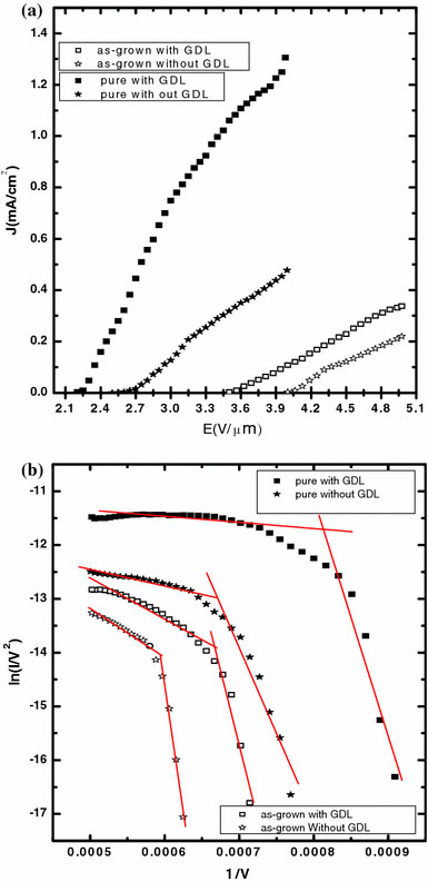
Figure 4a shows the field emission current density as a function of applied field for samples A, B, C and D. The corresponding Fowler–Nordheim (FN) plots are shown in Fig. 4b. Field emission by the samples have been analyzed using the Fowler–Nordheim theory, according to which emission current density (J) of a metal tip is expressed as a function of the local electric field (Elocal) and the work function (Φ) of the emitter tip. i.e.
Figure 4.

(a) Field emission characteristics of as-grown MWNT spin coated over carbon paper with and without graphitic layer (sample A and sample B) and that of purified MWNT spin coated over carbon paper with and without graphitic layer (sample C and sample D), (b) Fowler–Nordheim plots of as-grown MWNT spin coated over carbon paper with and without graphitic layer (sample A and sample B) and that of purified MWNT spin coated over carbon paper with and without graphitic layer (sample C and sample D)
where B = 6.83 × 10⁹ V eV−3/2 m−1. In the present case, for all the samples, emission occurs from multiple emitters and hence the measured current is an average of currents due to individual emitters. The exact analysis of field emission characteristics of the samples is a tedious task, as the work function of the individual emitters may be different. Also the local field on each emitter tip may vary. The local field Elocalis related to the macroscopic applied field E by a dimensionless geometrical enhancement factor (β) as
The value of β has been determined from the slope of the FN plot using the relation
where d is the distance of the anode from the emitting surface. The work function of the nanotube is assumed to be 5.0 eV (that of graphite) for comparison of the samples. The turn-on field, i.e. the applied field at which emission current density becomes 10 μA/cm2, the threshold field at an emission current density of 0.2 mA/cm2 and the field enhancement factor β, for the samples are listed in Table 1. Sample C shows superior emission properties compared to samples A, B and D and this can be attributed to both the purity of the MWNT and the presence of the graphitized layer between the nanotubes and carbon paper in Sample C. The absence of the graphitized layer between the MWNT and carbon paper in samples B and D adversely affects their performance. Moreover, for samples A and B, the presence of catalytic impurities leads to weak adhesion of CNTs to the substrate, which results in their poor performance.
Table 1.
Comparative field emission characteristics of sample A, sample B, sample C and sample D coated over carbon paper
| Sample | βL | βH | Turn-on (10 μA/cm2) field(V/μm) | Threshold field at 0.2 mA/cm2(V/μm) |
|---|---|---|---|---|
| A |
548 |
3,995 |
3.51 |
4.38 |
| B |
322 |
6,066 |
4.01 |
4.94 |
| C |
1,389 |
15,881 |
2.3 |
2.85 |
| D | 1,199 | 12,266 | 2.59 | 3.15 |
It is clearly seen from Fig. 4b that for all the four samples, the FN plot has two distinct slopes. The slope in the high field region is much lower than that in the low field regime. This current saturation behavior at high field regime may be attributed to a number of mechanisms [1,12,23,24]. Among them are vacuum space charge effect, changes in local density of states at the emitter’s tip, solid state transport, interaction among adjacent tubes and adsorption/desorption of gaseous species even under high vacuum conditions due to emission assisted surface reaction processes [25-27].
The current stability of the samples was monitored continuously for a period of 4 h at a current density of 0.2 mA/cm−2. The emission current remained fairly constant for samples A and C. The fluctuation in emission current for sample A was within 4% and that of sample C was within 1%. This indicates that there is an improvement in the field emission characteristics upon purification of MWNT. In the case of the other two samples (B and D), fluctuations were very high. Visual inspection of the samples after the current stability studies revealed that the morphology of the samples A and C remain intact and that of samples B and D got damaged. Also, the emission characteristics of samples A and C were exactly reproducible after the current stability studies, which reveal that the average number of active emission sites of the samples remains fairly constant throughout the study. The weak adhesion of CNTs to the substrate due to the absence of the graphitized layer is responsible for the damage of samples B and D. However, in order to bring out the exact dynamics behind the emission process further studies are required.
Conclusions
MWNT with a purity of 95% have been prepared by the pyrolysis of acetylene over DyNi2alloy hydride catalyst by CVD technique. Fully carbon based field emitters have been fabricated by spin coating a solution of MWNT and dichloroethane (DCE) over carbon paper with and without graphitic layer. The field emission properties of CNT film prepared by spin coating of the purified MWNT–DCE solution over graphitized carbon paper are superior compared to the other samples, due to the purity of the carbon nanotubes and the presence of the graphitic layer which provides better adhesion between the CNTs and the substrate. It shows excellent field emission properties with a fairly stable emission current over a period of 4 h. All the samples show current saturation effects. The use of graphitized carbon paper as substrate opens several new possibilities for CNT field emitters, with reduced contact resistance.
Acknowledgement
The authors are grateful to IITM and DRDO for financial assistance. One of the authors, R.B Rakhi wishes to thank Council of Scientific and Industrial Research (CSIR) India, for the financial assistance provided in the form of a senior research fellowship.
References
- Bonard JM, Salvetat JP, Stockli T, Forro L, Chaelain A. Appl. Phys. A. 1999. p. 245. COI number [1:CAS:528:DyaK1MXls1KmtbY%3D] [DOI]
- Kyung S, Lee Y, Kim Lee CJ, Yeom G. Carbon. 2006. p. 1530. COI number [1:CAS:528:DC%2BD28XjvFShs7c%3D] [DOI]
- Cheng Y, Zhou O. C.R. Physique. 2003. p. 1021. COI number [1:CAS:528:DC%2BD3sXptlGmsLg%3D] [DOI]
- Chen SY, Miao HY, Lue JT, Ouyang MS. J. 2004. p. 273. COI number [1:CAS:528:DC%2BD2cXpsVWnsQ%3D%3D] [DOI]
- Sheng LM, Liu M, Liu P, Wei Y, Liu L, Fan SS. Appl. 2005. p. 9. COI number [1:CAS:528:DC%2BD2MXot1Wnu7s%3D] [DOI]
- Bethune DS, Kiang CH, de Vries MS, Gorman G, Savoy R, Vazquez J, Beyers R. Nature. 1993. p. 605. COI number [1:CAS:528:DyaK3sXltVOrs7s%3D] [DOI]
- Guo T, Nikolaev P, Thess A, Colbert DT, Smalley RE. Chem. 1995. p. 49. COI number [1:CAS:528:DyaK2MXnvFWisLg%3D] [DOI]
- Yudasaka M, Kikuchi R, Matsui T, Ohki Y, Yoshimura SE, Ota SE. Appl. 1995. p. 2477. COI number [1:CAS:528:DyaK2MXovVGktr0%3D] [DOI]
- M.M. Shaijumon, S. Ramaprabhu. Chem Phys Lett. 374(5–6), 513 (2003)
- Ren ZF, Huang ZP, Xu JW, Wang JH, Bush P, Siegal MP. Science. 1998. p. 1105. COI number [1:CAS:528:DyaK1cXntlarurs%3D] [DOI] [PubMed]
- Choi WB, Chung DS, Kang JH, Kim HY, Jin YW, Han IT. Appl. 1999. p. 3129. COI number [1:CAS:528:DyaK1MXnt12qs7w%3D] [DOI]
- Bonard JM, Salvetat JP, Stockli T, de Heer WA, Forro L, Chaelain A. Appl. 1998. p. 918. COI number [1:CAS:528:DyaK1cXltVSmsb0%3D] [DOI]
- Choi WB, Jin YW, Kang JH, Kim HY, Lee SJ. Appl. 2001. p. 1547. COI number [1:CAS:528:DC%2BD3MXhslWju74%3D] [DOI]
- Lim SC, Choi HK, Jeong HJ, Song YI, Kim GY, Jung KT, Lee YH. Carbon. 2006. p. 2809. COI number [1:CAS:528:DC%2BD28XoslGnsLg%3D] [DOI]
- Jeong HJ, Choi Kim HK GY, Song YI, Tong Y, Lim SC, Lee YH. Carbon. 2006. p. 2689. COI number [1:CAS:528:DC%2BD28XoslGns74%3D] [DOI]
- Mauricio Roselen Patrick Poa J CH, Tronto Simone, Marchesin Marcel S, Ravi S, Silva P. Chem. 2006. p. 151. COI number [1:CAS:528:DC%2BD28XltV2gtbg%3D] [DOI]
- S. Uemura, J. Yotani, T. Nagasako, H. Kurachi, H. Yamada, T. Ezaki et al., in Field emission display, vol. 33 (The Society for Information Display, 2002), p. 1132.
- Park JH, Choi JH, Moon JS, Kushinov DG, Yoo JB, Park CY. Carbon. 2005. p. 698. COI number [1:CAS:528:DC%2BD2MXhtFGks7c%3D] [DOI]
- Shaijumon MM, Bijoy N, Ramaprabhu S. Appl. 2005. p. 192. COI number [1:CAS:528:DC%2BD2MXktFKktA%3D%3D] [DOI]
- Chiang IW, Brinson BE, Smalley RE, Margrave JL, Hauge RH. J. 2001. p. 1157. COI number [1:CAS:528:DC%2BD3MXislyitA%3D%3D] [DOI]
- R.B. Rakhi, K. Sethupathi, S. Ramaprabhu Int. J. Hydrogen Energy (2007), in press.
- Gao XP, Qin X, Wu F, Liu H, Lan Y, Fan SS, Yuan HT, Song DY, Shen PW. Chem. 2000. p. 271. COI number [1:CAS:528:DC%2BD3cXmt1ent7Y%3D] [DOI]
- Williams MV, Begg E, Bonville L, Kunz HR, Fenton JM. J. 2004. p. 1173. COI number [1:CAS:528:DC%2BD2cXmt1Slt7g%3D] [DOI]
- Dong C, Gupta MC. Appl. 2003. p. 159. COI number [1:CAS:528:DC%2BD3sXltFKisb0%3D] [DOI]
- Dean KA, Chalamala BR. Appl. 2000. p. 375. COI number [1:CAS:528:DC%2BD3cXksVChtg%3D%3D] [DOI]
- Collins PG, Zettl A. Phys. 1997. p. 9391. COI number [1:CAS:528:DyaK2sXivVWrs70%3D] [DOI]
- Srivastava SK, Vankar VD, Rao DVS, Kumar V. Thin Solid Films. 2006. p. 1851. COI number [1:CAS:528:DC%2BD28Xht1WqsrzM] [DOI]


