Abstract
The growth of para-sexiphenyl (6P) thin films as a function of substrate temperature on Ir{111} supported graphene flakes has been studied in real-time with Low Energy Electron Microscopy (LEEM). Micro Low Energy Electron Diffraction (μLEED) has been used to determine the structure of the different 6P features formed on the surface. We observe the nucleation and growth of a wetting layer consisting of lying molecules in the initial stages of growth. Graphene defects – wrinkles – are found to be preferential sites for the nucleation of the wetting layer and of the 6P needles that grow on top of the wetting layer in the later stages of deposition. The molecular structure of the wetting layer and needles is found to be similar. As a result, only a limited number of growth directions are observed for the needles. In contrast, on the bare Ir{111} surface 6P molecules assume an upright orientation. The formation of ramified islands is observed on the bare Ir{111} surface at 320 K and 352 K, whereas at 405 K the formation of a continuous layer of upright standing molecules growing in a step flow like manner is observed.
Keywords: Graphene, Low energy electron microscope (LEEM), Self-assembly, Organic thin film, Sexiphenyl(6P), LEED, Iridium
Highlights
► Para-sexiphenyl growth on graphene and Ir was observed in real time using LEEM. ► The structure of individual 6P features was analyzed using μLEED. ► At 320 K and 352 K Stranski–Krastanov growth of flat lying 6P is found on graphene. ► Islands formed by upright standing molecules are found on Ir(111). ► At 405 K only propagation of upright 6P islands, nucleated at graphene rims on Ir.
1. Introduction
In recent years, the growth of organic semiconductors on solid substrates has received significant attention for both scientific and technological reasons. One such organic semiconductor is para-sexiphenyl (6P), a rigid rod-like conjugated molecule. Thin film growth of 6P molecules has been investigated intensely due to the unique optical and electronic properties of the molecule. These properties are found to be subject to substrate anisotropy and also depend on the arrangement of the molecules in a thin film [1,2]. The molecular orientation can be controlled by using appropriate substrates from lying [3] to upright standing [4]. In-depth knowledge of the growth behavior as a function of temperature is a key to controlling the thin film structure and exploiting its full technological potential [5]. In several recent publications it has been shown how the growth parameters can be used to tailor the morphology of 6P thin films on different substrates [6–8]. In this paper, we investigate the growth and structure of 6P molecules at different surface temperatures on epitaxially grown graphene sheets supported by an Ir{111} surface. The layers and needles that form on graphene as well as the ramified structures that grow on Ir{111} are studied as a function of substrate temperature. The role of defects in the graphene sheets is also analyzed using Low Energy Electron Microscopy (LEEM) and Photoemission Electron Microscopy (PEEM). Micro Low Energy Electron Diffraction (μLEED) is used to locally obtain structural information [9].
2. Experimental
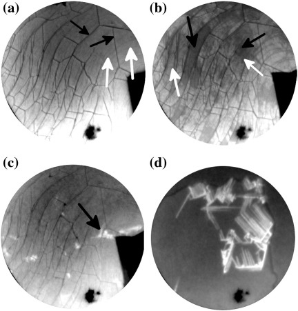
The experiments are carried out in an Elmitec LEEM III apparatus of Bauer's design [10] with a base pressure of less than 1 × 10− 10 mbar. A 1.4 μm field-limiting aperture has been utilized to collect local structural information from features of interest. An Ir{111} substrate is atomically cleaned by exposing to low pressures of O2 at elevated temperature. Graphene films are then prepared by Chemical Vapor Deposition (CVD) of ethylene (C2H4) on the Ir{111} surface at a temperature of 875 K [11]. The growth of the graphene flakes is followed in-situ using PEEM until sufficiently large graphene flakes have formed on the Ir{111} surface. A LEEM image of such a flake is shown in Fig. 1(a). Substrate steps (thin lines, indicated by white arrows) are still visible in Fig. 1(a) as the graphene flake follows the topographic contours of the underlying substrate. A network of straight linear features (indicated by black arrows), appearing much darker and wider than the steps, is also visible on the graphene. These linear features are wrinkles in the graphene sheet that result from elastic relaxations that occur when the sample is cooled from the graphene growth temperature to the 6P deposition temperature. The wrinkles extend about 3 nm from the surface and are a few nanometers in width [12]. Commercially available 6P molecules in powder form are deposited by Organic Molecular Beam Epitaxy (OMBE) from a Knudsen-cell type evaporator that is held at a temperature of 553 K for all described experiments. From previous experiments it was calibrated to yield an average growth rate of 6.3 × 10− 4 6P/(nm2s). This corresponds to a growth rate of 2.7 ML/h of flat lying 6P molecules [13]. We use the term monolayer for a closed layer of molecules having the mentioned structure. The number of 6P molecules per surface atom varies between 0.015 6P/graphene and 0.28 6P(100)/Ir{111}, consequently only deposition times and molecular densities are given. The sample temperature during deposition of 6P has been varied between 320 K and 405 K. In what follows we will refer to this as the deposition temperature. These deposition temperatures are precise relative to each other. However, thermal effects in the sample holder might lead to a small but unknown offset of all temperatures given throughout the text.
Fig. 1.
LEEM images acquired at a temperature of 320 K with an electron energy of 2.7 eV for (a)–(c) and 3.7 eV for (d). The Field of View (FoV) is 6 μm for (a)–(c) and 4 μm for (d). Times indicated are measured with respect to the start of 6P deposition. (a, t = 0 s) A single graphene flake on the Ir{111} surface is imaged prior to exposure to 6P. Graphene wrinkles (indicated with black arrows) and the faint contours of Ir{111} surface steps (indicated with white arrows) are visible on the single layer graphene flake. (b, t = 813 s, 0.52 6P/nm2) The graphene flake is covered by a wetting layer of 6P. The two additional grey levels correspond to the initial layer formed by flat lying face-on molecules only (white arrows), and the final wetting layer with a face-on/edge-on, like structure (black arrows). The nucleation of this film happens next to the wrinkles. (c, t = 1268 s, 0.80 6P/nm2) Bright crystallites occur on top of the wetting layer next to the wrinkles (black arrow). (d, t = 2149 s, 1.36 6P/nm2) Parallel needles continue to grow with ongoing deposition. The dark area in the lower part of the images is a defect in the channel plate.
3. Results and discussion
3.1. Deposition of 6P at 320 K
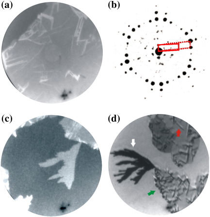
A sequence of bright field LEEM images acquired during the deposition of 6P molecules is shown in Fig. 1. Fig. 1(a) shows the pristine graphene surface with graphene wrinkles (thick straight lines) and steps in the underlying Ir{111} surface (thin curved lines). For a detailed discussion of the morphology of graphene flakes on Ir{111} the reader is referred to [11,12,14]. With the deposition of 6P molecules, the intensity of reflected electrons from the graphene decreases, indicating the presence of a diluted phase of 6P molecules on the surface. After 727 s (0.46 6P/nm2) of deposition, nucleation of 6P domains takes place next to the wrinkles. The domains are mobile and move over the graphene surface [15]. After 813 s (0.52 6P/nm2) of deposition, the intensity that is measured on 6P domains reduces even further (indicated by black arrows in Fig. 1(b)). The dark 6P domains grow to form a complete monolayer after 948 s (0.60 6P/nm2) of 6P deposition. For the next 130 s no new features or significant contrast changes are observed. After this, bright 6P crystallites can be observed. These crystallites also nucleate next to the wrinkles, as indicated by the black arrow in Fig. 1(c). In contrast to the initial islands, these crystals are immobile. With continued deposition, they elongate, resulting in a fiber like morphology. Fig. 1(d) shows a LEEM image after stopping 6P growth at 2149 s (1.36 6P/nm2). The graphene surface is covered by a 6P wetting layer of monolayer thickness and long fiber-like structures, which nucleated either from defects in the wetting layer caused by the wrinkles, or from other needles.
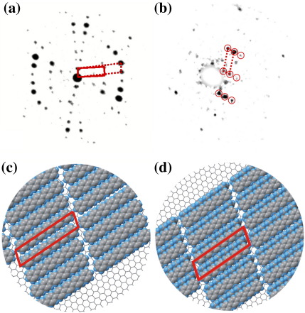
Fig. 2(a) shows a μLEED pattern that is obtained from an area without needles which is only covered by the monolayer thick wetting layer. The μLEED pattern consists of the specular reflection surrounded by several rings of LEED spots. It reveals an ordered molecular structure. Within the 1.4 μm aperture that we used to obtain the μLEED pattern several different rotational domains are present. Careful analysis of the μLEED pattern also shows that the 6P molecules are arranged in two different ways, in other words there are two different phases present. The unit cells are highlighted with solid and dotted lines. The length of the unit cell vectors, highlighted with dashed lines, are 5.2 Å and 27.8 Å at an angle β of 72°. Here, β is the angle between the two lattice vectors. The angle Θ between the long axis of the 6P unit cell and the graphene unit cell vector is 79°. The dimensions of the unit cell vectors, highlighted with solid lines, are 8.3 Å and 27.8 Å at an angle β of 70°. Taking into account distortions in the LEED pattern this numbers are accurate within 5%. In accordance with the results obtained at 240 K [13] we assume that the first small unit cell contains one molecule in a face-on configuration (Fig. 2(c)), while the second larger unit cell contains two molecules which are assembled in a face-on / edge-on arrangement (Fig. 2(d)). The latter arrangement is similar to the one found in the surface unit cell of the bulk 6P plane [16]. Also the size of the unit cell is similar to the bulk surface unit cell. However, the underlying substrate does not allow the film to relax completely. This results in a larger spacing along the long molecular axis. We obtain the following matrix notations for the unit cell vectors of the adsorbate lattice in terms of the substrate lattice vectors (a = b = 2.46 Å and α= 120°): for the initial layer while the final bulk like layer has a matrix notation of . These latter values show a good match with structural data ( for the final layer) obtained at a much lower temperature of 240 K [13]. The fact that this relationship between the 6P layer and graphene does not change over a temperature range of at least 80 K is a strong hint towards a fixed relationship between the two. Keeping in mind the accuracy of our initial measurements we therefore interpret this as a coincidence type II quasiepitaxial relationship [17]. In fact a 5×10 superstructure describes the layer more accurately. Taking into account the superstructure we arrive at the following matrix notations for the initial and the final monolayer thick wetting layer . This also better reflects the fact that in the superstructure the flexible molecules are free to relax their orientation and position in the superstructure by small amounts.
Fig. 2.
(a) μLEED pattern measured from graphene covered with one monolayer of 6P at an electron energy of 14 eV. The specular reflection and other LEED spots associated with various rotational domains of the ordered 6P structure are visible. (b) μLEED pattern measured from a graphene area covered by needles at an electron energy of 21 eV. The LEED spots are marked with red circles to guide the eyes. (c) Molecular arrangement corresponding to the dashed unit cell in (a). The unit cell contains one face-on molecule. (d) Sketch of the molecular arrangement corresponding to the solid unit cell in (a). Two molecules per unit cell in an alternating face-on / edge-on configuration are found here. The molecular arrangement in the needles (b) is similar to this second denser phase present in the wetting layer.
A typical μLEED pattern taken from needles is shown in Fig. 2(b). It consists of LEED spots from a single domain and thus reveals an ordered molecular structure. The dimensions of the unit cell vectors are 9.5 Å and 26.9 Å at an angle β of 69°. The molecular arrangement is similar to the second denser phase found in the wetting layer (Fig. 2(d)). Again these values are very similar to the size of the 6P surface unit cell and the size of the bigger unit cell found in the wetting layer. However, the three dimensional shape of the fiber crystallites allows the unit cell to relax towards the bulk value.
The growth of 6P on graphene at 320 K can be summarized by the following four steps. (1) An initial layer of only flat lying molecules is formed on the graphene surface. This layer nucleates next to the wrinkles. (2) When a critical coverage is reached, the initial layer transforms into a bulk like layer (Fig. 1(b)). The molecules obtain a flat face-on / edge-on configuration similar to the 6P plane. (3) 6P fibers nucleate on top of the monolayer thick wetting layer (Fig. 1(c)). This nucleation occurs next to the wrinkles. (4) Parallel bundles of needles grow away from the wrinkles (Fig. 1(d)). The needles have the same orientation as the underlying wetting layer. The azimuthal orientation of the long needle axis is roughly perpendicular to the azimuthal orientation of the long unit cell axis and the long molecular axis.
Nearly all nucleation events are occurring next to the wrinkles. The change in curvature of the graphene next to the wrinkle, strain in the adsorbed 6P islands, and the high mobility are responsible for the preferred nucleation of the wetting layer next to wrinkles and the observed large domain size, which is in the μm range. The preferred nucleation, mobility, and formation of the initial wetting layer of 6P on graphene are discussed in detail elsewhere [13,15]. The wrinkles – by creating a large network of 1D defects in the 6P wetting layer – are responsible for the preferred nucleation of the needles next to them.
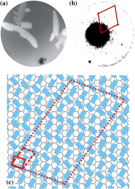
Although the graphene flakes cover extended areas of the Ir{111} surface, they still do not cover the entire surface. The remaining bare Ir{111} surface areas are inspected after stopping the deposition of 6P molecules (1.36 6P/nm2). LEEM images show the presence of irregularly shaped 6P structures, as presented in Fig. 3(a). A μLEED measurement obtained from a branch of one of the irregularly shaped structures is shown in Fig. 3(b). The μLEED pattern reveals that 6P molecules form an ordered structure on the Ir{111} surface. The dimensions of the nearest neighbor cell vectors are 5.0 Å by 5.0 Å at an angle β of 108°. The size of this nearest neighbor cell implies that in these irregularly shaped structures the long axis of the molecules is roughly perpendicular to the surface. However, the cell vectors given above are the nearest neighbor distances and not the real unit cell vectors. This is a consequence of the molecular form factors for the two differently rotated upright standing molecules being nearly identical. The unit cell vectors are: 5.0 Å by 9.1 Å at an angle β of 105° and Θ= 25° (). Considering the above mentioned measurement precision and the fact that some of the molecules will shift slightly to reach a more favorable position, a 5×5 superstructure with a matrix notation of (a coincidence type II quasiepitaxial relationship [17]) describes the situation more accurately. This can be seen in Fig. 3(c) where some of the molecules would need to be shifted only slightly by fractions of an Ångstrom to reach a well coordinated site. The 6P molecules are arranged in a similar (up-right standing) fashion as in the (100) plane of the 6P bulk crystal. Different 6P islands or arms of them can have different azimuthal crystallographic orientations. This has been made visible in Fig. 3(a) by using a slightly off normal incident of the electron beam. As a result different crystallographic orientations show different intensities similar to a dark field image. μLEED patterns recorded away from the irregular structures consist only of Ir{111} spots and a dominant diffuse background. The latter is attributed to an unordered 2D gas phase layer of 6P present on the surface of the Ir.
Fig. 3.
(a) LEEM image of irregularly shaped structures of 6P grown on the Ir{111} surface. The Ir{111} surface appears dark and the ramified 6P islands show different shades of grey. (FoV: 15 μm, electron energy: 3.5 eV, deposition temperature: 320 K) (b) μLEED pattern obtained from one of the islands at an electron energy of 19.4 eV. The nearest neighbor cell is highlighted by red lines. (c) The structural model proposed from the μLEED pattern shown in (b). The molecules are arranged in up-right standing orientation on Ir{111}. Nearest neighbor cell, unit cell and the 5×5 superstructure are indicated by red lines (solid, dashed, and dotted respectively).
It is well known that on clean metal surfaces para-n-phenyl oligomers prefer a lying configuration [18–20]. However, small amounts of surfactants will lead to an upright standing configuration of the molecules [19–22]. Therefore, it is reasonable to assume that carbon residues of the graphene growth are causing the appearance of these irregularly shaped structures on Ir{111}.
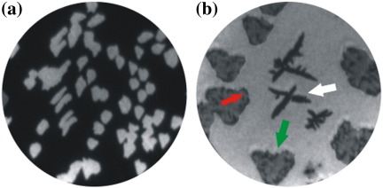
PEEM relies on photo-emitted electrons and therefore depends on changes in the work function of a sample to create image contrast. The clean Ir{111} surface appears dark, since its work function (5.76 eV [23]) is higher than the photon energy (4.9 eV) whereas the graphene (4.8 eV–4.9 eV [24]) flakes appear bright (Fig. 4(a)). However, after deposition of 6P the Ir{111} surface appears brighter than graphene (Fig. 4(b)). The change in contrast is suggestive of a surface work function variation caused by 6P adsorption and the formation of an interface dipol – both on Ir{111} and graphene. The 6P needles grown on graphene (indicated by a red arrow) appear darker than the 6P wetting layer on the graphene (Fig. 4(b)). A white arrow is indicating the irregularly shaped structures on the Ir{111} surface which gives a relatively darker contrast. The 6P covered graphene flakes appear darker than Ir{111} and have lighter shade of grey than the 6P needles. Therefore, the resulting order in brightness (from low to high) of the materials roughly grouped by work function is: Ir{111} and upright standing 6P islands on Ir{111} (both higher or similar to the photon energy), 6P-needles, 6P wetting layer on graphene, disordered 6P on Ir{111}. The non-emitting 6P needles are therefore only visible because they sit on a brighter background. This is similar to the contrast mechanism observed for the case of 6P/Cu(110) 2×1-O [25].
Fig. 4.
(a, t = 205 s) 100 μm FoV PEEM image of Ir{111} covered with graphene flakes. The Ir{111} surface appears dark, since its work function (5.76 eV) is higher than the photon energy (4.9 eV). (b, t = 2149 s) 50 μm FoV PEEM image acquired after 6P deposition at a temperature of 320 K. The 6P structures, graphene flakes, and ramified islands on Ir{111} are marked with red, green, and white arrows, respectively. Times indicated are measured with respect to the start of ethylene (C2H4) and 6P deposition, respectively.
3.2. Measurements at 352 K
Increasing the deposition temperature to 352 K, leads to no principle changes in the film formation process. After the initial two-step formation of a wetting layer – by nucleation of domains near the wrinkles – the growth of parallel needles sets in. Again the needles nucleate either near the wrinkles, or from existing needles creating comb like structures (Fig. 5(a)). As expected, higher deposition temperatures and the resulting enhanced mobility of 6P leads to fewer, but longer needles [26].
Fig. 5.
(a, t = 2130 s, 1.35 6P/nm2) 10 μm FoV LEEM image acquired at an electron energy of 2.7 eV and 352 K. A single graphene flake on the Ir{111} surface is imaged after deposition of 6P. The edge of the graphene flake is visible in the upper left part. The graphene flake is covered with 6P needles of different orientation. (b) μLEED pattern measured from graphene covered by the wetting layer at an electron energy of 19.3 eV. (c) 20 μm FoV LEEM images acquired at an electron energy of 2.7 eV and a temperature of 352 K. The Ir{111} surface with an irregular shaped island and three graphene flakes covered with 6P is visible. The 6P island on the Ir{111} surface is connected to the graphene flake. (d) 50 μm FoV PEEM image acquired after stopping the 6P deposition. 6P needles, graphene flakes, and 6P islands on Ir are present and marked by red, green, and white arrows, respectively (352 K).
A typical μLEED pattern measured from the graphene surface covered by the wetting layer is shown in Fig. 5(b). The μLEED pattern consists of the specular beam reflection surrounded by several rings of LEED spots. This μLEED pattern is similar to the one obtained at 320 K presented in Fig. 2(a). The structure of the wetting layer at this elevated temperature is identical to the one that was already found for the growth at 320 K. Due to the small signal, no reliable structural information could be obtained from the needles. However, taking into account the similarities in the wetting layer and the comparable morphology, one can conclude their structure is similar to the structure at 320 K presented in Fig. 2(d).
Post-deposition (2130 s, 1.35 6P/nm2) LEEM imaging of the Ir{111} surface reveals the presence of branched 6P structures (Fig. 5(c)). All 6P structures on Iridium nucleate at the edges of the graphene flakes. The increased mobility of 6P on Ir{111} at this high temperature requires the stable graphene flakes for nucleation. Once formed, they act as sinks for all 6P diffusing on the Ir{111} surface. A similar structure of upright molecules as observed for the other deposition temperatures is proposed.
A PEEM image acquired after stopping the deposition of 6P is shown in Fig. 5(d). The 6P needles on the graphene flake (indicated with a red arrow) appear darker than the 6P wetting layer in the same way as described above. A white arrow marks the irregular and branched structures on the Ir{111} surface. Again, they show a darker contrast than the surrounding surface. The 6P wetting layer on the graphene flakes itself shows an intermediate grey level.
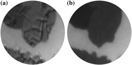
Post deposition annealing of the film leads to a decay of the structures. From deposition temperature to 381 K 6P structures on graphene and Ir{111} remain intact and immobile (Fig. 6(a)). With a further increase of temperature, first the small and later also the bigger needles start to decay until at 400 K all structures on the flakes have disappeared (Fig. 6(b)). The excess molecules can diffuse off the graphene flake into the 2D gas phase on the supporting Ir{111} substrate. A further increase of temperature results in a shrinking of the – so far unchanged – irregularly shaped structures on the Ir{111} surface. They eventually disappear all at 416 K. When comparing these results to desorption data obtained on other substrates [19,27], uncertainties of the temperature measurements in the LEEM sample holder as well as the low heating rate of only 6 K/min have to be taken into account. The sequence in which 6P desorbs from the different substrates is further evidence underlining the weak interaction of 6P with graphene.
Fig. 6.
(a, T = 381 K) PEEM image acquired after stopping the 6P deposition. The 6P needles, on two graphene flakes can be seen. (b, T = 401 K) The same two graphene flakes are cleared from all 6P needles. (FoV: 26 μm).
3.3. Measurements at 405 K
Fig. 7 is a sequence of images recorded during 6P deposition at 405 K.
Fig. 7.
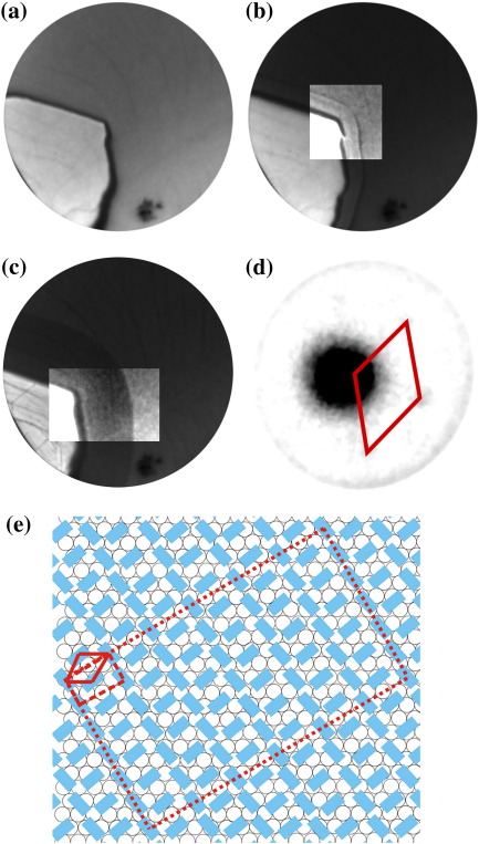
6 μm FoV LEEM images acquired at an electron energy of 2.7 eV and temperature of 405 K. (a, t = 0 s) A graphene flake residing on the Ir{111} surface prior to exposure to 6P. Wrinkles and the contours of Ir{111} surface steps are visible on the single layer graphene flake. (b, t = 831 s, 0.53 6P/nm2) The nucleation of a 6P film takes place on the edges of the graphene flake, as is witnessed by the appearance of a band of different intensity at the edge of the graphene (see contrast enhanced center). The reflected intensity from the Ir{111} surface decreases. Three different levels of contrast are found. From left to right: graphene, ordered 6P layer and 6P lattice gas on Ir{111}. (c, t = 1391 s, 0.88 6P/nm2) The ordered 6P film extending from the graphene flake has grown further (see contrast enhanced center). (d) A μLEED pattern is measured at electron energy of 25.6 eV using a 1.4 μm field-limiting aperture from the Ir{111} surface area completely covered with the ordered 6P layer. The nearest neighbor cell is highlighted by red lines. (e) The structural model proposed from the μLEED pattern shown in panel (d). The molecules are arranged in an up-right standing orientation on Ir{111}. The unit cell (dashed lines) and the nearest neighbor cell (solid line) are shown. The 6×6 superstructure is indicated by a dotted line. Times indicated are measured with respect to the start of 6P deposition.
Fig. 7(a) shows the initial situation. The reflected intensity from the Ir{111} surface decreases with deposition time, indicating the presence of a diluted phase of 6P on the surface. However, at this elevated temperature neither the formation of a wetting layer, nor the nucleation of any other 6P structure is observed on graphene. We believe, that the already large diffusion length of 6P at lower temperatures (i.e. as low as 240 K [13]), will be of the order of the radius of the graphene flakes (roughly 2 μm) at 405 K. As a result, the 6P molecules diffuse from the flakes onto the Ir{111} surface, where 6P domains nucleate at the edges of the graphene flake. This process begins after 230 s (0.14 6P/nm2) of deposition (Fig. 7(b) and (c)). The contrast enhanced centers of Fig. 7(b, c) allow to distinguish between the graphene flake (left and brightest), ordered 6P film and 6P gas phase (upper right). However, the borders between the different areas (in particular in Fig. 7(b)) are affected by a LEEM image artefact related to abrupt changes in morphology and work function [28].
A μLEED pattern obtained from the dark band next to graphene flake in Fig. 7(c) on the 6P covered Ir{111} surface is shown in Fig. 7(d). Only very diffuse spots can be found, superimposed on a homogeneous, diffuse background. The crystalline quality of this film is not very high. The nearest neighbor cell highlighted in Fig. 7(d) has a size of 5.0 Å by 5.0 Å with an angle β of 120°. The obvious way to accommodate the 6P molecules into such a small space is in an upright standing way where the long molecular axis is roughly perpendicular to the substrate. Using the unit cell of the bulk (100) plane (8.091 Å by 5.568 Å and β = 90° [16]) as a starting point we can deduct the unit cell of 6P on Ir{111} to be 8.7 Å by 5 Å and β and Θ = 90° (dashed line in Fig. 7(e)). Compared to the bulk structure this unit cell is compressed along the short axis. The resulting matrix notation of the overlayer with respect to the underlying Ir{111} is given by the following quasiepitaxial coincidence type II relationship [17] . Using the same arguments as for the previous structures a 6×6 superstructure describes the situation more precisely and results in the following matrix notation which is depicted in Fig. 7(e). The distortion of the 6P unit cell is geometrically justified as the molecular rows will have the substrate dictated 120° angle. μLEED patterns obtained far away from the flakes show only the unordered 2D gas phase of 6P. Different to the well investigated [29–31], but non-metallic system – 6P on TiO2 – we see no evidence for an additional ordered layer of flat lying molecules [32].
In general, increased substrate temperatures have been identified as one of the reasons for the growth of up-right standing 6P molecules [7,33,34]. In the same way, the elevated surface temperature of Ir{111} favors the growth of up-right standing 6P thin films. No other structures – neither on Ir{111} nor on graphene – were found for this deposition temperature.
4. Summary and conclusions
The deposition of 6P molecules and growth of 6P structures on graphene has been studied at different temperatures. For sample temperatures during deposition up to 352 K, wrinkles in the graphene act as preferential nucleation sites for both, a wetting layer and 6P needles with the same crystallographic orientation. The 6P needles form after the completion of the wetting layer. This is usually identified as the Stranski–Krastanov growth mode, often observed for 6P films formed from flat lying molecules [3].
Defects of the Ir{111} substrate – a result of carbon residues after the formation of the graphene flakes – are nucleation sites for the growth of ramified structures consisting of upright standing 6P molecules. However, with increasing sample temperature (compare Fig. 1(d) at 320 K to Fig. 5(a) at 352 K), less but longer 6P needles are formed on graphene. In addition 6P nucleation on the Ir{111} surface gets increasingly difficult and ramified islands of upright 6P are exclusively nucleated at the rim of graphene flakes. Further increase of the deposition temperature to 405 K results in a considerable change of growth behavior. Neither a wetting layer, nor any three dimensional needles are observed on graphene. A 6P(100) layer does, however, nucleate at the edges of the graphene flakes. It grows on the Ir{111} surface in a step flow-like fashion. This layer built from upright standing molecules shows poor crystallinity.
Our study illustrates that at all temperatures investigated, the growth behavior of 6P on graphene and Ir{111} is governed by defects. Up to 352 K, graphene wrinkles dictate the nucleation and growth behavior of the 6P wetting layer, and needles. At 405 K, the edges of the graphene flakes are the sites where 6P domains develop on Ir{111}.
Acknowledgement
This work was financially supported by the Austrian Science Fund (FWF) project N9707-N20, STW, and is part of the research program of the Foundation for Fundamental Research on Matter, which is financially supported by the Netherlands Organization for Scientific Research.
References
- 1.Niko A., Meghdadi F., Ambrosch-Draxl C., Vogl P., Leising G. Synth. Met. 1996;76:177. [Google Scholar]
- 2.Mikami T., Yanagi H. Appl. Phys. Lett. 1998;73:563. [Google Scholar]
- 3.Teichert C., Hlawacek G., Andreev, Sitter H., Frank P., Winkler A., Sariciftci N.S. Appl. Phys. A. 2006;82:665. [Google Scholar]
- 4.Hlawacek G., Puschnig P., Frank P., Winkler A., Ambrosch-Draxl C., Teichert C. Science. 2008;321:108. doi: 10.1126/science.1159455. [DOI] [PubMed] [Google Scholar]
- 5.Yang F., Shtein M., Forrest S.R. Nat. Mater. 2004;4:37. [Google Scholar]
- 6.Kintzel E.J., Smilgies D.M., Skofronick J.G., Safron S.A., Van Winkle D.H. J. Vac. Sci. Technol., A. 2004;22:107. [Google Scholar]
- 7.Müllegger S., Hlawacek G., Haber T., Frank P., Teichert C., Resel R., Winkler A. Appl. Phys. A. 2007;87:103. [Google Scholar]
- 8.Lengyel O., Šatka A., Haber T., Kovać, Sitter H., Resel R. Cryst. Res. Technol. 2008;43:44. [Google Scholar]
- 9.Bauer E. Surf. Rev. Lett. 1998;5:1275. [Google Scholar]
- 10.Bauer E. Rep. Prog. Phys. 1994;57:895. [Google Scholar]
- 11.Coraux J., N'Diaye A.T., Engler M., Busse C., Wall D., Buckanie N., Meyer zu Heringdorf F.J., van Gastel R., Poelsema B., Michely T. New J. Phys. 2009;11:023006. [Google Scholar]
- 12.N'Diaye A.T., van Gastel R., Martínez-Galera A.J., Coraux J., Hattab H., Wall D., Meyer zu Heringdorf F.J., Horn von Hoegen M., Gómez-Rodríguez J.M., Poelsema B., Busse C., Michely T. New J. Phys. 2009;11:113056. [Google Scholar]
- 13.Hlawacek G., Khokhar F.S., van Gastel R., Poelsema B., Teichert C. Nano Lett. 2011;11:333. doi: 10.1021/nl103739n. [DOI] [PMC free article] [PubMed] [Google Scholar]
- 14.van Gastel R., N'Diaye A.T., Wall D., Coraux J., Busse C., Buckanie N.M., Meyer zu Heringdorf F.J., Horn von Hoegen M., Michely T., Poelsema B. Appl. Phys. Lett. 2009;95:121901. [Google Scholar]
- 15.Hlawacek G., Khokhar F.S., van Gastel R., Teichert C., Poelsema B. IBM J. Res. Dev. 2011;55:15. doi: 10.1021/nl103739n. [DOI] [PMC free article] [PubMed] [Google Scholar]
- 16.Baker K., Fratini A., Resch T., Knachel H., Adams W., Socci E., Farmer B. Polymer. 1993;34:1571. [Google Scholar]
- 17.Hooks D.E., Fritz T., Ward M.D. Adv. Mater. 2001;13:227. [Google Scholar]
- 18.Winter B., Ivanco J., Netzer F.P., Ramsey M.G. Thin Solid Films. 2003;433:269. [Google Scholar]
- 19.Müllegger S., Winkler A. Surf. Sci. 2006;600:1290. [Google Scholar]
- 20.Hlawacek G., Teichert C., Müllegger S., Resel R., Winkler A. Synth. Met. 2004;146:383. doi: 10.1063/1.1767154. [DOI] [PubMed] [Google Scholar]
- 21.Resel R., Oehzelt M., Haber T., Hlawacek G., Teichert C., Müllegger S., Winkler A. J. Cryst. Growth. 2005;283:397. [Google Scholar]
- 22.Winter B., Berkebile S., Ivanco J., Koller G., Netzer F.P., Ramsey M.G. Appl. Phys. Lett. 2006;88:253111. [Google Scholar]
- 23.Strayer R., MacKie W., Swanson L. Surf. Sci. 1973;34:225. [Google Scholar]
- 24.Starodub E., Bostwick A., Moreschini L., Nie S., Gabaly F.E., McCarty K.F., Rotenberg E. Phys. Rev. B. 2011;83:125428. [Google Scholar]
- 25.Fleming A.J., Netzer F.P., Ramsey M.G. J. Phys. Condens. Matter. 2009;21:445003. doi: 10.1088/0953-8984/21/44/445003. [DOI] [PubMed] [Google Scholar]
- 26.Balzer F., Rubahn H.G. Surf. Sci. 2004;548:170. [Google Scholar]
- 27.Winter B., Ivanco J., Netzer F.P., Ramsey M.G., Salzmann I., Resel R. Langmuir. 2004;20:7512. doi: 10.1021/la049529q. [DOI] [PubMed] [Google Scholar]
- 28.Schertz F., Kutnyakhov D., Schuppler S., Nagel P., Nepijko S., Schönhense G. Appl. Phys. A. 2011;102:253. [Google Scholar]
- 29.Resel R., Oehzelt M., Lengyel O., Haber T., Schulli T., Thierry A., Hlawacek G., Teichert C., Berkebile S., Koller G. Surf. Sci. 2006;600:4645. [Google Scholar]
- 30.Hlawacek G., Teichert C., Andreev A.Y., Sitter H., Berkebile S., Koller G., Ramsey M., Resel R. Phys. Status Solidi (A) 2005;202:2376. [Google Scholar]
- 31.Berkebile S., Koller G., Hlawacek G., Teichert C., Netzer F.P., Ramsey M.G. Surf. Sci. 2006;600:L313. [Google Scholar]
- 32.Sun L., Berkebile S., Weidlinger G., Koller G., Hohage M., Netzer F.P., Ramsey M.G., Zeppenfeld P. Phys. Chem. Chem. Phys. 2010;12:3141. doi: 10.1039/b922285e. [DOI] [PubMed] [Google Scholar]
- 33.Athouel L., Froyer G., Resel R., Koch N., Meghdadi F., Leising G. Synth. Met. 1999;101:627. [Google Scholar]
- 34.Haber T., Müllegger S., Winkler A., Resel R. Phys. Rev. B. 2006;74:045419. [Google Scholar]


