Abstract
Although tremendous progress has been made in organic light-emitting diodes (OLEDs), with few exceptions they are fabricated in the standard way by sequentially depositing active layers and electrodes onto a substrate. Here we describe a different approach for building OLEDs, which is based on physical lamination of thin metal electrodes supported by an elastomeric layer against an electroluminescent organic. This method relies only on van der Waals interactions to establish spatially homogeneous, intimate contacts between the electrodes and the organic. We find that devices fabricated in this manner have better performance than those constructed with standard processing techniques. The lamination approach avoids forms of disruption that can be introduced at the electrode/organic interface by metal evaporation and has a reduced sensitivity to pinhole or partial pinhole defects. In addition, because this form of “soft” contact lamination is intrinsically compatible with the techniques of soft lithography, it is easy to build patterned OLEDs with feature sizes into the nanometer regime. This method provides a new route to OLEDs for applications ranging from high performance displays to storage and lithography systems that rely on subwavelength light sources.
Organic optoelectronic materials enable new classes of devices that could be important for consumer electronics. Organic light-emitting diodes (OLEDs) (1, 2), for example, form the basis of ultrathin and power efficient mechanically flexible display systems. In addition, miniaturized devices that have features in the micro- and nanometer regime also have the potential to be important for applications in photonics, chem/biosensing, and other areas. There are significant technical and scientific challenges associated with building high-performance devices of this type and with understanding the details of their behavior. In particular, the nature of the interface between an organic semiconductor and a metal electrode is critical to the performance of these as well as other organic electronic and optoelectronic devices such as photovoltaic cells (3) and transistors (4). It is known that evaporation of metals onto organics, which represents the most common way to establish electrical contacts, leads to in-diffusion of the metal, changes in the morphology of the organic, and, in some cases, disruption of chemical bonds (5, 6). These effects are important because they can lead to the generation of luminescence quenching centers in OLEDs (5–7) and large interfacial resistances in transistors (8). The interfaces are difficult to control, however, because they depend sensitively on complex chemical and physical interactions between the metal and the organic, and also on the detailed processing conditions. A new technique, soft contact lamination (ScL) (3, 8, 9), provides a means for establishing electrical contacts at room temperature in ambient conditions without the externally applied pressures and heating that are associated with other lamination techniques (4, 10) or the disruption of the organic that can be associated with evaporation. It thereby minimizes chemical, physical, and morphological changes to the organic. This paper shows that the OLEDs built with this ScL method outperform identical devices produced by direct evaporation. Measurements of current–voltage characteristics, photoluminescence (PL), and electroluminescence (EL) provide some information that may partly explain the improved performance. The paper concludes by demonstrating that these good characteristics persist in micrometer- and nanometer-scale OLEDs fabricated by the combined use of ScL and soft lithographic techniques, including a form of near-field optical lithography to define electrodes with dimensions of ∼150 nm. Facile large area nano-patterning of the flexible electrode and the ability to modify the physical and chemical properties of the top electrode are both important features that the ScL technique brings to the area of high-performance, f lexible nanooptoelectronic devices.
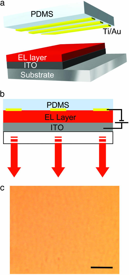
Fig. 1 schematically illustrates an OLED fabricated by ScL. The ScL device consists of two parts: a transparent elastomeric element coated with a thin metal film and a transparent substrate that supports an electrode and a film of an electroluminescent organic. When these two components are brought together, van der Waals interactions pull them into intimate contact to complete the device. This soft, laminated contact is robust (i.e., the device can be turned upside down without the pieces coming apart), reversible (i.e., the components can be peeled apart with no visual damage to either) and can be established at room temperature without any applied pressure. The elastomer that we use for the experiments is PDMS (Sylgard 184, Dow-Corning) cast and cured (60°C for 3 h) against the flat surface of a silicon wafer. Exposing the PDMS (typical thickness between 1 and 5 mm) to an oxygen plasma (∼2 s, 30 standard cm3/min, 30 mT, 100 V; Plasma-Therm reactive ion etcher) followed by electron beam evaporation at ∼5 × 10⁻⁷ torr (1 torr = 133 Pa) of ∼1-nm Ti (adhesion promoter; 0.3 nm/s) and 20- to 60-nm Au (1 nm/s) generates thin electrically continuous metal films that are strongly bonded to the PDMS. [We use Au in these studies because, unlike the more typical materials such as Ca and Al, it does not chemically interact with most organics and does not form a surface oxide. These features greatly simplify the interpretation of device characteristics. Certain other metals can be used (for example, Pd can be evaporated on top of PDMS with the same procedures used for Au, and Al and Ag can be evaporated on top of Au/PDMS).] Evaporating through a shadow mask placed near the PDMS enables coarsely patterned OLEDs. Micrometer and nanoscale devices can be achieved by using various soft lithographic methods. Spin casting forms a uniform film of the electroluminescent material on a thin (∼100 nm) layer of ITO (∼15 Ω per square) on a glass slide (0.4 mm thick). When the bottom and top pieces are brought together, van der Waals forces pull the electrodes into intimate contact with the EL layer at room temperature, without application of external pressure. Typically this contact initiates on one side of the structure; a wetting front then progresses naturally across the sample until the entire surface is in contact. We typically observed, using an optical microscope, perfect contact (i.e., absence of any air gaps) over large areas (see Fig. 1c). In all cases, the metal-coated PDMS was either used to build devices immediately after evaporation or after removal from brief storage in a dry nitrogen environment.
Fig. 1.
Schematic illustration of OLEDs formed by ScL. (a) A piece of the elastomer poly(dimethylsiloxane) (PDMS) supports thin conducting electrodes of Ti (1 nm)/Au (20–60 nm), and a transparent substrate supports an electroluminescent (EL) layer on indium tin oxide (ITO). (b) When these pieces are brought together, van der Waals forces pull the electrodes into intimate contact with the EL layer at room temperature, without application of external pressure. (c) A reflection image taken with an optical microscope on lamination of Au/PDMS on the EL layer. (Scale bar, 50 μm.)
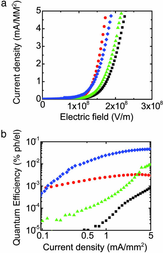
We first compare the performance of OLEDs built by ScL and by direct evaporation of Au electrodes (conventional devices) onto thin (∼65 nm) films of poly[2-methoxy-5-(2′-ethylhexyloxy)-1,4-phenylenevinylene] (MEH-PPV; MW 90000, H. W. Sands, Jupiter, FL) spin cast onto ITO/glass. The Au was evaporated on MEH-PPV at a relatively high rate of 10 Å/s by electron beam with a long distance (∼30 cm) between the metal source and the sample, and with a rotating sample mount (5). The current and light output of these devices were measured while biasing the voltage positively to either the ITO or the Au. Qualitatively, the emission from both types of devices is spatially uniform as viewed by eye or through a microscope. Fig. 2a shows typical current–voltage behavior. The similar current–voltage characteristics, together with the uniform emission, suggest that the two types of devices have similar electrical properties. Fig. 2b displays typical external EL quantum efficiencies (11) as a function of current density. Because the work function of ITO [∼4.7 eV (1 eV = 1.602 × 10⁻¹⁹ J)] is smaller than that of Au (∼5.1 eV), the efficiencies are higher when Au is biased positively than when ITO is biased positively because of enhanced electron injection. In contrast to the similar electrical properties, the ScL devices have efficiencies that are larger [maximum quantum efficiency: 0.015% ph/el for ITO-positive direction and 0.056% ph/el for Au-positive direction] than the conventional ones (maximum quantum efficiency: 0.0015% ph/el for ITO-positive direction and 0.003% ph/el for Au-positive direction).§ The quantum efficiencies of ScL devices with Au electrodes in both bias directions are also comparable to thermally evaporated ITO/MEH-PPV/Al devices with a lower work function metal (Al) that we fabricated (maximum quantum efficiency: 0.01% ph/el for ITO-positive direction and 0.04% ph/el for Al-positive direction) and previous reported values on similar Al devices (12, 13). Because the MEH-PPV is primarily a hole transporting material, most of the excitons form near the Au in both types of devices when the ITO is biased positively. Nonradiative energy transfer from these excitons to metal (i.e., luminescence quenching by metal) represents one mechanism that reduces the efficiency (14). This effect occurs in both conventional and ScL devices. The lower efficiency in the conventional devices suggests the presence of additional quenching mechanisms. These could arise from various pathways associated with metal indiffusion, changes in morphology, bond disruption, and other effects caused by deposition of the Au. The large difference in efficiency is also present when the Au is positively biased. Although most excitons in this case are generated near the ITO, they can readily diffuse toward the Au side of the device during operation because their characteristic diffusion length is ∼20 nm (15), which represents a substantial fraction of the thickness of the MEH-PPV. In addition, the peak recombination zone moves toward the Au electrode because of the enhancement of charge-carrier mobility in increasing electric fields (16). As a result, the excitons can be quenched through the same pathways, independent of the direction of the bias.
Fig. 2.
Characteristics of OLEDs formed from a stack of ITO (100 nm)/MEH-PPV (65 nm)/Au (20 nm), fabricated by ScL and by evaporation (conventional) of the Au layer. (a) Current density as a function of electric field. (b) External quantum efficiency [% photons per electron (ph/el)] as a function of current density. Squares, conventional device operated with ITO positively biased; triangles, ScL device operated with ITO positively biased; circles, conventional device operated with Au positively biased; diamonds, ScL device with Au positively biased. For both bias directions, the efficiency of the ScL device is much higher than that of the conventional device.
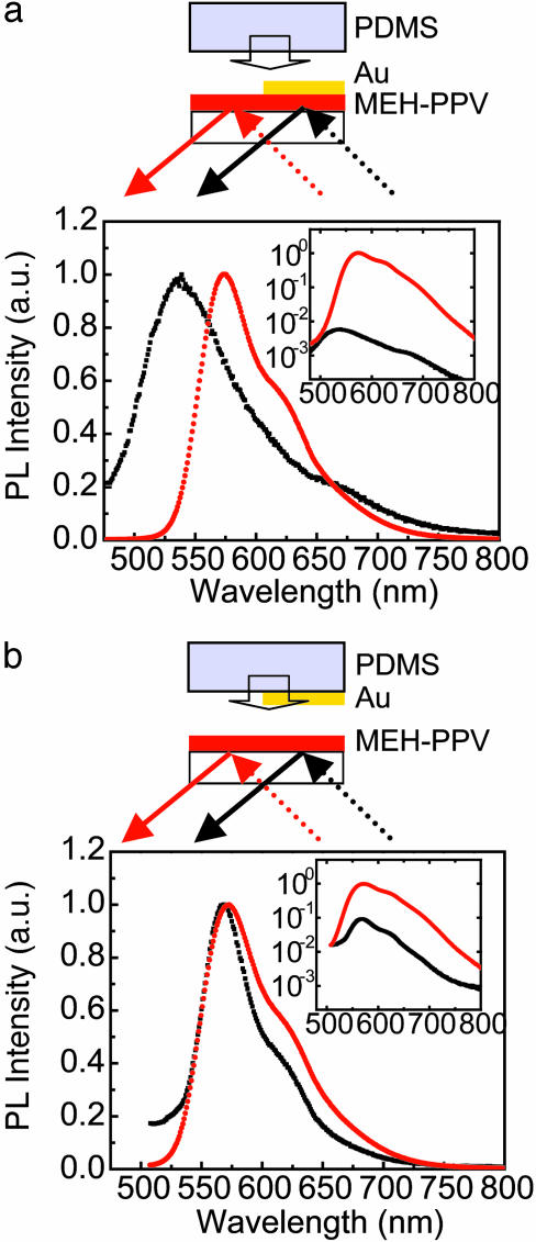
To provide additional insight into the differences in quantum efficiency between these two types of devices, we measured the PL spectra from test structures that consisted of ∼10-nm-thick MEH-PPV films spin cast onto glass slides. Half of the film in each case was covered by a layer of Au (20 nm thick) formed either by evaporation (Fig. 3a) or by ScL (Fig. 3b). Laminating a bare piece of PDMS against the evaporated sample makes it similar in construction to the ScL structure. Data were collected in the same reflection mode geometry for both samples. Fig. 3a Inset shows that the PL intensity in the evaporated structure is more than two orders of magnitude lower in the region coated with Au. More significantly, this reduced PL has a spectrum that is blue-shifted relative to MEH-PPV (Fig. 3a), suggesting disruption of the π–π conjugation of the polymer in the part of the sample that was evaporated with Au.¶ Fig. 3b shows, in contrast, that the ScL structures have PL spectra that are similar to those obtained from regions of the MEH-PPV that are not coated with Au. Furthermore, the PL intensity is only one order of magnitude smaller on the side that has laminated Au (Fig. 3b Inset). This decrease likely arises from simple metal quenching effects at the interface. It is reversible: removing the ScL electrode returns the PL intensity and spectrum to those characteristics of portions of the MEH-PPV that were never in contact with Au. From these results and the EL measurements, we conclude that detrimental effects at the interface of the evaporated device, which may include disruption of conjugation in the polymer chains and metal in-diffusion, lead to quenching that can reduce the device efficiency compared to those formed by ScL. Other reports describe quenching induced by interaction with secondary electrons in electron beam evaporators; these effects likely play a role here. It is also possible that different sensitivities to partial pinhole defects of ScL and evaporated electrodes contribute to different apparent device efficiencies.
Fig. 3.
Normalized and unnormalized (Insets) PL spectra. (a) PL spectra of 10-nm MEH-PPV films with evaporated Au coatings on half. In the main part of the graphs, the spectra were normalized to the maximum intensities of the PL from the bare regions of the MEH-PPV film (without Au), which were identical for both samples. (b) PL spectra of 10-nm MEH-PPV films with Au coatings formed by ScL on half of it. The films were excited at a wavelength of 420 nm in the uncoated and Au-coated regions by using the same excitation/detection geometry. The data taken from the bare MEH-PPV region are shown in red, and those taken from the Au-coated region are shown in black. The PL from the evaporated Au region is lower in intensity and blue-shifted compared to the regions that do not have Au. In contrast, PL from regions with laminated Au coatings show decreases in intensity but no spectral shift. In the main graphs, the PL intensities are normalized to the peak intensity of the bare film without Au coating.
Although the absolute efficiencies of even the ScL devices are relatively low when Au is used, the performance can be improved through various strategies. For example, blending organic salts [tetra-n-butylammonium tetrafluoroborate (TBABF4)] into the emitting polymer (MEH-PPV:TBABF4 = 0.865:0.135) produces field-induced dipoles that enhance hole and electron injections from both electrodes (17–19). For a single-layer ScL device made of 190-nm film of the MEH-PPV and TBABF4 blend with 60-nm Au/PDMS, a maximum external efficiency of 2.5% ph/el was measured at 3.4 V. Pure MEH-PPV ScL devices with 60-nm Au/PDMS can also be improved by depositing a thin (∼10 nm) electron injecting layer [the blend of poly(ethylene oxide) and TBABF4] onto MEH-PPV (2, 17–19). With this strategy, we obtained maximum external quantum efficiency of 0.53% ph/el at 6.8 V for ScL devices. ScL devices might also be improved by employing other proven methods used in conventional OLED devices (2). For example, low work function metals could be used in place of Au. This strategy, however, requires careful experimental control to avoid surface oxides that can form before or during lamination.
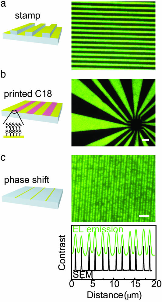
In addition to high efficiencies and noninvasive, reversible electrical contacts, ScL provides unique opportunities for using soft lithography to make patterned OLEDs with high resolution, in ways that might complement other reported techniques (20–23). Here we demonstrate three different approaches, using a polyfluorene derivative (24) as the electroluminescent layer because of its better stability than MEH-PPV: (i) the PDMS element itself can provide surface relief to pattern the contacts (Fig. 4a) (8, 9, 25), (ii) the Au on the PDMS can be chemically modified by microcontact printing patterns of insulating thiols (21, ∥) as barriers to charge injection (Fig. 4b), and (iii) photo-lithography with conformable phase masks (26) and etching can be used to pattern directly the Au on the PDMS with nanometer resolution (Fig. 4c). Each of these approaches achieves high contrast patterned emission by modifying the top electrode before lamination. The spatial homogeneity of the emission in the patterned areas is, in all cases, comparable to that of unpatterned devices formed by evaporation. We observed, however, much slower growth in the dark spots in ScL devices than evaporated ones. The nanopatterned OLEDs (Fig. 4c) have ∼150-nm-wide Au line electrodes but show emission profiles of ∼600-nm linewidth, which is comparable to the resolution of the optical imaging system. The efficiency of these nanodevices is nearly as good (0.23% ph/el with 20-nm Au) as unpatterned ones (0.65% ph/el). Ultrasmall, flexible OLEDs such as these could potentially be useful, for example, as conformable light sources for subwavelength storage or lithography systems, or nanoscale optoelectronics. These and other more conventional applications, as well as fundamental investigations of electrode/organic semiconductor interfaces, represent some of the many promising areas of use for ScL.
Fig. 4.
Patterned OLEDs formed by the combined use of ScL and soft lithography. In all cases, the Au was 20 nm thick and the electroluminescent layer was a polyfluorene derivative blended with 17 wt % of TBABF4 (100 nm). The unpatterned devices showed EL efficiencies of 0.65% ph/el. The schematic illustrations on the left show the modifications to the ScL electrodes, and the images on the right represent an example of OLEDs fabricated by using the approach. (a) Molding features of relief into the PDMS followed by blanket deposition of the electrode generates emission in the pattern of the raised features. (Scale bar, 100 μm.) (b) Microcontact printing an insulating self-assembled monolayer (octadecanethiol; C18) before lamination yields emission only in the bare Au regions. (Scale bar, 100 μm.) (c) Photolithography with a conformable phase mask followed by etching directly patterns lines (150 nm wide) of Au on the PDMS. The averaged linewidth (∼600 nm) of the pattern of emission (graph below) in this case is comparable to the resolution of the optical imaging system. (Scale bar, 5 μm.) The Rayleigh diffraction limit for the 0.55-numerical-aperture microscope objectives is 590 nm at a wavelength of 540 nm. The EL image was taken through the ITO (100 nm)/glass (0.4 mm), which reduces the effective numerical aperture.
In summary, organic/polymer EL devices formed by ScL exhibit homogeneous physical contacts and improved quantum efficiency compared to conventional devices. This latter feature may result, at least partly, because ScL avoids the detrimental effects caused by metal evaporation that give rise to nonradiative decay channels for excitons. In addition to excellent performance, micro- and nanoscale devices based on chemical or physical modification of the top electrodes before lamination demonstrates the power of ScL for fabricating high-resolution organic optoelectronic devices.
Acknowledgments
We thank B. Acharya for technical help with the microscope and J. Kim for helpful comments. T.-W.L. thanks the Korea Science and Engineering Foundation for partial financial support. J.Z. thanks the Dr.-Jürgen-Ulderup Foundation for financial support.
This paper was submitted directly (Track II) to the PNAS office.
Abbreviations: EL, electroluminescence; ITO, indium tin oxide; MEH-PPV, poly[2-methoxy-5-(2′-ethyl-hexyloxy)-1,4-phenylenevinylene]; OLED, organic light-emitting diode; PDMS, poly(dimethylsiloxane); ph/el, photons per electron; PL, photoluminescence; ScL, soft contact lamination; TBABF4, tetra-n-butylammonium tetrafluoroborate.
Footnotes
For comparison, a thermally evaporated device of the same structure with Au electrode showed 5.9 × 10⁻⁵% quantum efficiency for ITO-positive direction and 1.6 × 10⁻⁴% quantum efficiency for Au-positive direction.
The degree of quenching rates and blue shift in spectra because of bond disruption depends on the evporation method (electron beam or thermal), the evaporation rate, and the molecular weight and chemical structures of the material, etc.
We put high-concentration (5 mM) octadecanethiol solution on the patterned stamp to generate high-contrast patterned images.
References
- 1.Tang, C. W. & Van Slyke, S. A. (1987) Appl. Phys. Lett. 51, 913–915. [Google Scholar]
- 2.Friend, R. H., Gymer, R. W., Holmes, A. B., Burroughes, J. H., Marks, R. N., Taliani, C., Bradley, D. D. C., Dos Santos, D. A., Brédas, J. L., Lögdlund, M. & Salaneck, W. R. (1999) Nature 397, 121–128. [Google Scholar]
- 3.Granström, M., Petritsch, K., Arias, A. C., Lux, A., Andersson, M. R. & Friend, R. H. (1998) Nature 395, 257–260. [Google Scholar]
- 4.Loo, Y.-L., Someya, T., Baldwind, K. W., Bao, Z., Ho, P., Dodabalapur, A., Katz, H. E. & Rogers, J. A. (2002) Proc. Natl. Acad. Sci. USA 99, 10252–10256. [DOI] [PMC free article] [PubMed] [Google Scholar]
- 5.Faupel, F., Willecke, R. & Thran, A. (1998) Mater. Sci. Eng. R 22, 1–55. [Google Scholar]
- 6.Birgerson, J., Fahlman, M., Bröms, P. & Salaneck, W. R. (1996) Synth. Met. 80, 125–130. [Google Scholar]
- 7.Choong, V.-E., Park, Y., Gao, Y., Wehrmeister, T., Müllen, K., Hsieh, B. R. & Tang, C. W. (1997) J. Vac. Sci. Technol. A 15, 1745–1749. [Google Scholar]
- 8.Zaumseil, J., Baldwin, K. W. & Rogers, J. A. (2003) J. Appl. Phys. 93, 6117–6124. [Google Scholar]
- 9.Zaumseil, J., Someya, T., Bao, Z., Loo, Y.-L., Cirelli, R. & Rogers, J. A. (2003) Appl. Phys. Lett. 82, 793–795. [Google Scholar]
- 10.Guo, T.-F., Pyo, S., Chang, S.-C. & Yang, Y. (2001) Adv. Funct. Mater. 11, 339. [Google Scholar]
- 11.Greenham, N. C., Friend, R. H. & Bradley, D. D. C. (1994) Adv. Mater. 6, 491–494. [Google Scholar]
- 12.Parker, I. D. (1994) J. Appl. Phys. 75, 1656–1666. [Google Scholar]
- 13.Lee, T.-W. & Park, O. O. (2000) Appl. Phys. Lett. 76, 3161–3163. [Google Scholar]
- 14.Becker, H., Burns, S. E. & Friend, R. H. (1997) Phys. Rev. B 56, 1893–1905. [Google Scholar]
- 15.Savenije, T. J., Warman, J. M. & Goossens, A. (1998) Chem. Phys. Lett. 278, 148–153. [Google Scholar]
- 16.Zhang, F., Wang, Y., Yang, X., Hou, Y., Xu, Z., Xu, X., Zhang, R. & Huang, Z. (2000) J. Lumin. 87–89, 1149–1151. [Google Scholar]
- 17.Lee, T.-W., Lee, H.-C. & Park, O. O. (2002) Appl. Phys. Lett. 81, 214–216. [Google Scholar]
- 18.Sakuratani, Y., Asai, M., Tokita, M. & Miyata, S. (2001) Synth. Met. 123, 207–210. [Google Scholar]
- 19.deMello, J. C., Tessler, N., Graham, S. C. & Friend, R. H. (1998) Phys. Rev. B 57, 12951–12963. [Google Scholar]
- 20.Veinot, J. G. C., Yan, H., Smith, S. M., Cui, J., Huang, Q. & Marks, T. J. (2002) Nano Lett. 2, 333–335. [Google Scholar]
- 21.Koide, Y., Such, M. W., Basu, R., Evmenenko, G., Cui, J., Dutta, P. Hersam, M. C. & Marks, T. J. (2003) Langmuir 19, 86–93. [Google Scholar]
- 22.Kim, C. S., Burrows, P. E. & Forrest, S. R. (2000) Science 288, 831–833. [DOI] [PubMed] [Google Scholar]
- 23.Rogers, J. A., Bao, Z. & Dhar, L. (1998) Appl. Phys. Lett. 73, 294–296. [Google Scholar]
- 24.Bernius, M. T. & Inbasekaran, M. (2000) Adv. Mater. 12, 1737–1750. [Google Scholar]
- 25.Schmid, H., Wolf, H., Allenspach, R., Riel, H., Karg, S., Michel, B. & Delamarche, E. (2003) Adv. Funct. Mater. 13, 145–153. [Google Scholar]
- 26.Rogers, J. A., Paul, K. E., Jackman, R. J. & Whitesides, G. M. (1997) Appl. Phys. Lett. 70, 2658–2660. [Google Scholar]


