Abstract
High-density stretchable electronics is achieved using multilayer interconnects on an elastomeric substrate. Two major challenges associated with stretchable electronics—increasing integration density and improving electrical bonding—have been addressed by our innovative multilayer via-bonding technology. The resulting multichip-module architecture provides an elastic, high-density solution for numerous potential applications.
Keywords: Stretchable electronics, multilayer interconnect, bonding, polydimethylsiloxane (PDMS), multichip module (MCM)
In recent years, interest has developed for implementing electronics using flexible, foldable, and even stretchable materials; the potential applications of such technologies include consumer products ranging from flexible/elastic displays to skin-like electronics.[1] Although it remains impractical to fabricate electronic components directly using soft materials, it is possible to connect an array of (rigid) component and subcircuit islands using flexible/stretchable interconnects to achieve system-level flexibility or conformability.[1,2] The components can be interconnected via a compliant substrate[1-5] or via a wiring mesh.[6-8] One of the primary challenges associated with the implementation of these systems is the limitation to integration density of the electronics when only a single layer of interconnect is used. To address this limitation, dual-layer interconnects have been fabricated (e.g., on flexible parylene substrates).[9] Another major challenge is the achievement of robust electrical connections between the soft material and rigid components or substrate. This bonding issue has significantly hindered the practical utility of flexible/stretchable electronics.
We have addressed these two challenges to create stretchable electronics by developing fabrication techniques that enable reliable multilayer interconnects both within an elastic polydimethylsiloxane (PDMS) substrate and between the PDMS and a rigid substrate. This interconnect technology addresses the challenge of integration density by providing multiple layers of wiring in the flexible PDMS device. The PDMS–to–rigid-substrate interconnect facilitates robust, high-density electrical connections between the two materials. Taken together, these two integral parts facilitate a new high-density bonding method called via bonding. This multilayer via-bonding technology facilitates high-density, module-level integration of electronic components in an integrated multilayer composite.
The key to our via-bonding technology is the combination of a lift-off method, which requires an anisotropic metal-deposition process, with an innovative inclined-via technique. Fig. 1 illustrates the method for fabricating multilayer interconnects within PDMS or between PDMS and another substrate. Such lift-off methods—because of their cleanness and process compatibility—are conventionally used in the patterning of thin-film metal features on PDMS.[10,11] In order to implement multilayer interconnects both within PDMS and between PDMS and another substrate, we have created a process for fabricating vias with inclined sidewalls through the PDMS. The inclined sidewalls are essential to provide electrical connections between the conductors on different layers. Because we use a lift-off method [Fig. 1(a)], we must use anisotropic metal deposition to create the gold conductors on the PDMS. Vias with vertical sidewalls would fail to make electrical connections between conducting layers because the anisotropic deposition would not result in metal on the sidewalls. The thin gold film deposited on the recessed slope of inclined vias, however, functions to electrically bridge two conducting layers.
Figure 1.
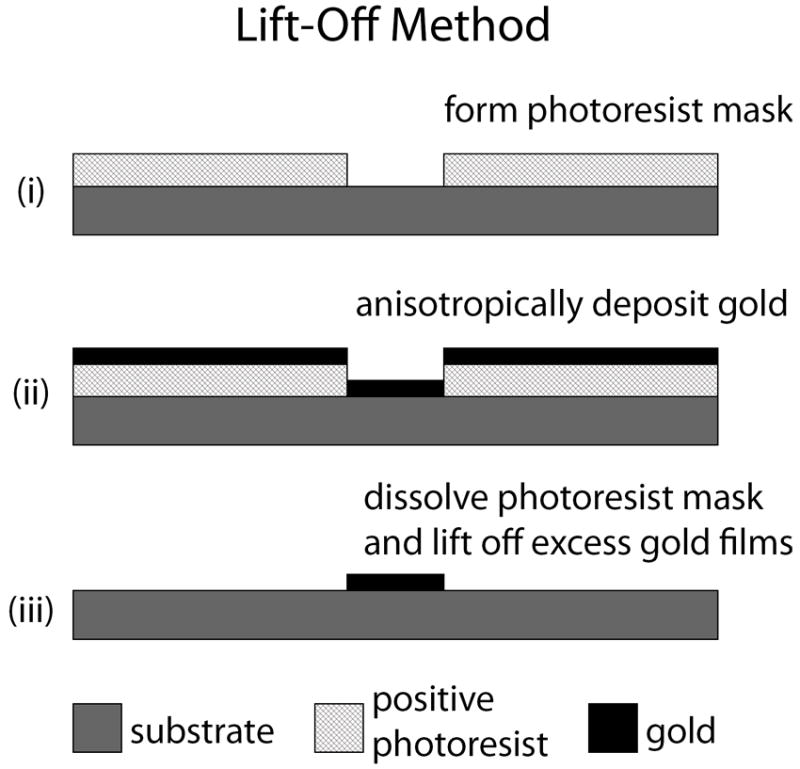
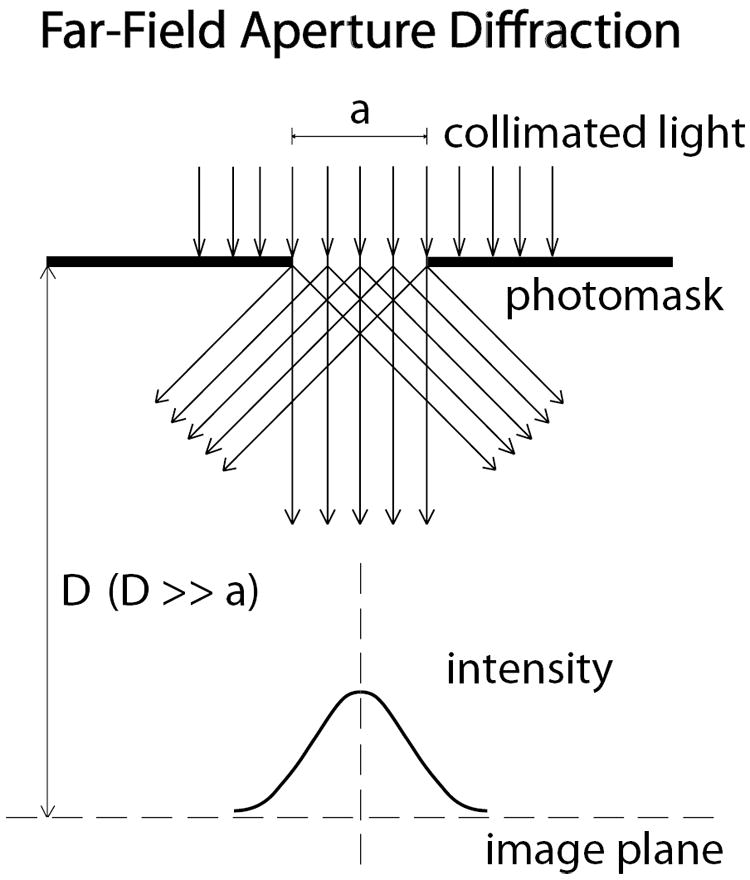
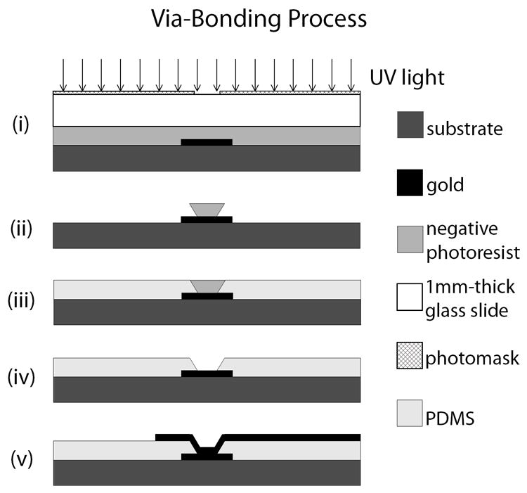
Method for implementing multilayer interconnects within PDMS or between PDMS and another substrate. (a) Process flow of a lift-off method for patterning thin-film metal features. (i) First, a photoresist mask is patterned on the substrate. (ii) Second, a thin metal film is deposited through an anisotropic metal deposition process (e.g., electron beam evaporator). (iii) Last, the sample is soaked in solvent or solution. The photoresist mask starts to dissolve from the feature sidewalls where no metal exists, and subsequently excess metal films are lifted off, leaving the desired metal features. (b) Far-field aperture diffraction phenomenon. When collimated light passes through a micro-hole, the light beam diffracts at the edges and casts a Gaussian-like intensity profile on an image plane placed with a distance D (large compared to the diameter a of the hole) away from the photomask. The via-bonding process makes use of this phenomenon to create tapered sacrificial posts. (c) Fabrication process steps. (i) A thick negative photoresist layer on a sample is placed at the image plane 1 mm away from the photomask. (ii) The resulting exposure creates a tapered sacrificial post. (iii) The post is subsequently used to mold the PDMS insulation. (iv) Removal of the sacrificial post results in an inclined via in the PDMS. (v) When patterning the second conducting layer using the lift-off method illustrated in (a), the two conducting layers will be electrically interconnected by metal film deposited on the recessed slope of the inclined via.
To fabricate the inclined vias, we use projection exposure in photolithography, which involves far-field aperture diffraction[12] [Fig. 1(b)]. In this method, collimated light passing through a micro-hole (100μm diameter) diffracts and casts a Gaussian-like intensity profile on an image plane placed at a distance (>1mm) away from the photomask. When a thick negative photoresist layer is placed at the image plane, the exposure results in a tapered post. A similar approach has been used previously in backside exposure of thick negative photoresist to create tapered SU-8 pillars.[13] We use this configuration to modulate the UV light intensity distribution in the exposure process of thick negative photoresist to make sacrificial posts with a tapered shape. In Fig. 1(c)(i), when the thick negative photoresist layer is positioned at the image plane in Fig. 1(b), the exposure will result in such a tapered profile [Fig. 1(c)(ii)].
The tapered sacrificial post is used as a mold during the formation of the encapsulation PDMS layer [Fig. 1(c)(iii)], resulting in a complementary inclined via in the PDMS after the post is sacrificed [Fig. 1(c)(iv)]. Well-defined spinning and curing recipes ensure that the PDMS prepolymer disperses to a layer thickness smaller than the height of sacrificial posts and that the prepolymer clears off the top of sacrificial posts.[14] The second conducting layer is fabricated using the same lift-off method [Fig. 1(a)] as used for the first conducting layer; the two layers are electrically interconnected where an inclined via exists as result of the gold film deposited on the recessed slope of the inclined via [Fig. 1(c)(v)].
By iterating the steps in Fig. 1(c), additional interconnected conducting layers can be fabricated subsequently. The “substrate” denoted in Fig. 1(c) can be either PDMS or other rigid materials, such as silicon, glass, printed circuit board (PCB), etc. For a PDMS substrate, the multilayer interconnects are made within the PDMS. For rigid materials, via bonds are fabricated on the rigid substrate and subsequent multilayer interconnects are fabricated using PDMS layers to facilitate increased integration density.
We fabricated the inclined vias as shown in Fig. 2. We demonstrated that the sidewall slope of the sacrificial posts can be controlled by adjusting UV light exposure dose [Fig. 2(a)], as a result of the low contrast profile of light intensity on the image plane [Fig. 1(b)]. The resolution of the resulting devices is 10μm width for gold lines and 10μm base diameter for inclined vias (given a 10μm PDMS encapsulation layer). The aspect ratio of the inclined via (defined as the via base diameter vs. the via depth) must be between 5:1 and 1:5 to ensure successful fabrication and electrical performance.
Figure 2.
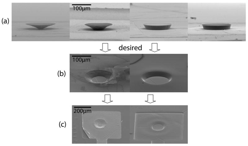
Fabrication results demonstrating the achievement of a multilayer interconnect by an inclined via. (a) Tapered sacrificial posts with different sidewall slopes were produced by using different UV light exposure doses. From left to right, the dose was increased. (b) Inclined vias with desired profiles were created in the PDMS insulation layer using the molding process. (c) The second gold layer was patterned using the lift-off process, and an interlayer interconnection (i.e. a via bond) was formed at the inclined via. After lift-off, a corner of the square gold film was lifted up intentionally to give a better visualization of the thin gold film (image on left). After gold deposition but before lift-off, the sidewalls of the photoresist mask can be seen clearly (image on right).
As shown in Fig. 3, we fabricated devices that include interconnections between three layers of wiring within the PDMS [Fig. 3(a) and Fig. 3(b)] and between the bottom wiring layer and a rigid glass substrate [Fig. 3(c)]. Gold traces embedded in the PDMS were interconnected to each other and to gold traces on the glass through inclined vias. Because PDMS cured on glass, silicon, or PCB bonds strongly to that substrate, the inclined-via–based interconnects (i.e. via bonds) between PDMS and the rigid substrate can form reliable high-density multilayer electrical connections on the rigid substrate. The total thickness of the device in Fig. 3(a) and Fig. 3(b) is 100μm, which includes a 70μm PDMS base layer and three 10μm PDMS insulation layers. The thin gold lines on different conducting layers are all 100μm wide. To verify the viability of the wiring and of the multilayer interconnect, we implemented circuits to power three LEDs, one connected to each wiring layer, and demonstrated the device’s ability to illuminate each LED and to withstand large deformation while maintaining its electrical functionality.
Figure 3.
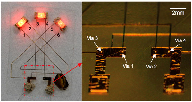
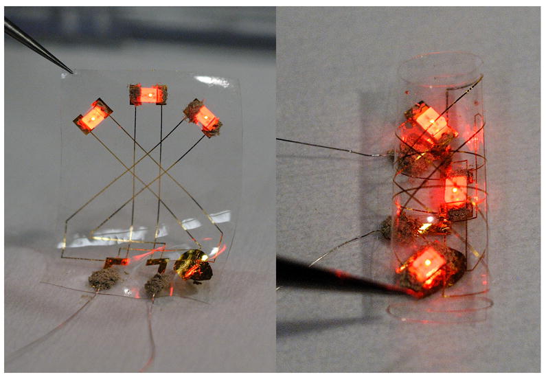
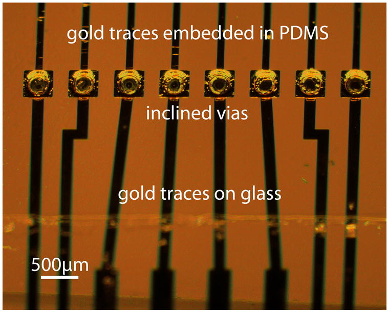
Demonstration of multilayer interconnects within PDMS and between PDMS and a rigid substrate. (a) A prototype device with three interconnected conducting layers. The total thickness of this device is 100μm, which includes a 70μm PDMS base layer and three 10μm PDMS insulation layers. The thin gold lines on different conducting layers are all 100μm wide. Three LEDs were glued using conductive polymer (Silicone Solutions; Twinsburg, OH) to their exposed contact pads on separate conducting layers. Power was supplied to the device through two silver wires glued to the contact pads on the bottom conducting layer. Traces 1 and 2 and power lines are on the bottom conducting layer; Traces 3 and 4 are on the middle conducting layer, and interconnected to the power lines through Vias 1 and 2, respectively; Traces 5 and 6 are on the top conducting layer, and interconnected to the power lines through Vias 3 and 4, respectively. Vias 3 and 4, both formed by two stacked inclined vias during two rounds of processes, go through two PDMS insulation layers, and thus are deeper than Vias 1 and 2. (b) Deformation of the device in (a). The device was scrolled into a roll while still maintaining its electrical functionality (right). (c) Via bonds on a rigid substrate (glass). Gold traces embedded in PDMS are interconnected to gold traces on glass through inclined vias. Only the bonding area is shown in this figure. In this area, PDMS was cured on bare glass. This formed a strong bonding between PDMS and the glass substrate.
High-density, elastic interconnect for electronics is one of the primary potential applications of our multilayer via-bonding technology. In Fig. 4, we show cross-sectional schematics for two example systems. Various components—including PCBs, prefabricated silicon integrated circuits (ICs), and thin film discrete components—embedded on multiple component layers can be connected electrically through multilayer via bonds to achieve a module-level circuit. The components can be stamped or printed on respective component layers. In the first example system [Fig. 4(a)], components are embedded and interconnected in PDMS to form stacked 3-D islands. This architecture can maximize the system-level stretchability similar to the electronic-skin architecture.[1,2] In the second example [Fig. 4(b)], embedded components are not stacked, resulting in decreased stretchability but increased design flexibility as a result of easier wire routing. The resulting elastic, multi-chip module (MCM) can interface with external circuits through exposed connections on the embedded PCBs. Such an elastic MCM may be rolled into a scroll or folded and thus forming a more compact 3-D circuit. Similar to the electronic skin architecture,[1,2] the elastic MCM can withstand mechanical deformation because the deformation is taken up largely by the exposed polymer substrate between the islands.[2] Because cured PDMS bonds to most rigid materials strongly (the bonding can be improved or strengthened by brief oxygen plasma treatment of the rigid substrate before applying PDMS coating), via bonds on the rigid components are expected to be strong enough to withstand a significantly large amount of strain, and thus should not be the locations for causing mechanical failure during deformation, as had previously been revealed by the study from Lacour et al. on “glued” components.[2] More detailed mechanical analyses are needed to determine the mechanical performance of such a multilayer composite during deformation.
Figure 4.

Architecture for an elastic, multichip module (not to scale). PCBs, prefabricated silicon ICs, and thin-film discrete components of various types can all be integrated into such a composite and interconnected using multilayer via-bonding technology to form a module-level circuit. (a) Components aggregate in stacked 3-D islands. This architecture can maximize the system-level stretchability. (b) Components are not stacked. This architecture gives more design flexibility.
In conclusion, two major challenges associated with stretchable electronics—(i) increasing integration density and (ii) improving electrical bonding—have been addressed by our innovative multilayer via-bonding technology. The resulting elastic MCM architecture provides a high-density, module-level solution for numerous potential applications.
Experimental
Lift-off Method
The sample is first briefly treated in oxygen plasma to activate the substrate [either cured PDMS (Sylgard 184, Dow Corning) or a rigid material] surface. Immediately following this treatment, positive photoresist [Megaposit SPR 220 (0.7 - 7.0), Shipley] is spun on at 1500 rpm for 30 seconds with a ramp rate of 300 rpm s-1. The sample is baked on a hotplate at 90°C for 10 minutes. The resulting photoresist layer is approximately 12μm thick. The sample is then patterned by photolithography with a UV exposure dose of 700 mJ cm-2 at 365nm i-Line, developed in developer (Microposit MF-319, Shipley) for about 160 seconds, rinsed with deionized water, and blown dry gently. Finally, the resulting photoresist negative mask is flood-exposed with the same dose to enable subsequent lift-off in its developer [Fig. 1(a)(i)]. A hold time of at least 120 minutes is required before starting depositing gold to allow water, which is necessary to complete the photo-reaction, to diffuse back into the photoresist mask. The sample is then placed in an electron beam evaporator for a priming layer of 300 Å titanium deposited at 1 Å s-1. This step is followed by a 200 Å to 5000 Å gold film deposition at 1 Å s-1 [Fig. 1(a)(ii)]. After deposition, the sample is soaked in the corresponding photoresist developer (Microposit MF-319, Shipley) to dissolve the photoresist mask and lift off excess gold films, leaving only the desired gold features [Fig. 1(a)(iii) or [Fig. 1(c)(v)]]. The gold patterned sample is then rinsed and dried.
Via-Bonding Process
Following brief treatment of the sample in oxygen plasma, a thick layer of negative photoresist (NR5-8000, Futurrex) is formed on the sample. The thickness of the layer depends on the lowest aspect ratio of the inclined via to be made. The sample is then patterned to leave a tapered sacrificial post right on top of each gold feature where an inclined via is to be made [Fig. 1(c), (i) and (ii)]. Next, following oxygen plasma treatment of the sample, a PDMS (Sylgard 184, Dow Corning) insulation layer is spun on to encapsulate the device at 5000 rpm for 150 seconds with a ramp rate of 1000 rpm s-1. Sequentially, the uncured sample is left at room temperature for one hour, baked on a 60°C hotplate for one hour, and then baked in a 90°C oven for two hours. The resulting encapsulation thickness is approximately 10μm, except at the areas closely surrounding the sacrificial posts [Fig. 1(c)(iii)]. To effectively remove the sacrificial posts, a brief RIE (Plasma Thermal Reactive Ion Etcher) descum process is first applied to remove any potential thin PDMS residues on top of sacrificial posts [15]. The sample is then immersed in acetone for approximately 10 minutes to remove the scrificial posts [Fig. 1(c)(iv)]. Finally, a lift-off process is used to pattern a new conducting layer to complete the via bonding [Fig. 1(c)(v)]. Two key points for creating the inclined via are worthy of emphasizing: (1) A 1mm glass slide is placed between the photomask and NR5-8000 layer [Fig. 1(c)(i)], and approximately 2/3 of standard exposure dose (i.e. 14 mJ cm-2 for 1μm-thick film) is used during UV exposure to create sacrificial posts with tapered sidewalls. Increasing or decreasing the exposure dose by 5/3 mJ cm-2 for 1μm-thick film each step within a certain range may result in tapered sacrificial posts with different sidewall slopes [Fig. 2(a)]. (2) The PDMS insulation layer is spun on immediately after oxygen plasma treatment of the sample. The recess depth of a via is determined by the height of the sacrificial post, and this height needs to be made slightly higher than the desired thickness of the PDMS insulation layer.
Acknowledgments
This research was supported by National Institutes of Health (NIH, Grant# EB006179), USA. The authors would like to thank E. Brown and Dr. J. Ross for providing valuable suggestions through discussions, and thank M. Kuykendal, D. Li, and A. C. Hughes for helping with editing the manuscript.
References
- 1.Wagner S, Lacour SP, Jones J, Hsu P-HI, Sturm JC, Li T, Suo Z. Physica E. 2004;25:326. [Google Scholar]
- 2.Lacour SP, Jones J, Wagner S, Li T, Suo Z. Proc of the IEEE. 2005;93:1459. [Google Scholar]
- 3.Ko HC, Stoykovich MP, Song J, Malyarchuk V, Choi WM, Yu C-J, Geddes JB, III, Xiao J, Wang S, Huang Y, Rogers JA. Nature. 2008;454:748. doi: 10.1038/nature07113. [DOI] [PubMed] [Google Scholar]
- 4.Kim D-H, Ahn J-H, Choi WM, Kim H-S, Kim T-H, Song J, Huang YY, Liu Z, Lu C, Rogers JA. Science. 2008;320:507. doi: 10.1126/science.1154367. [DOI] [PubMed] [Google Scholar]
- 5.Park S-I, Xiong Y, Kim R-H, Elvikis P, Meitl M, Kim D-H, Wu J, Yoon J, Yu C-J, Liu Z, Huang Y, Hwang K-C, Ferreira P, Li X, Choquette K, Rogers JA. Science. 2009;325:977. doi: 10.1126/science.1175690. [DOI] [PubMed] [Google Scholar]
- 6.Dinyari R, Rim S-B, Huang K, Catrysse PB, Peumans P. Appl Phys Lett. 2008;92:091114. [Google Scholar]
- 7.Someya T, Kato Y, Sekitani T, Iba S, Noguchi Y, Murase Y, Kawaguchi H, Sakurai T. Proc Natl Acad Sci USA. 2005;102:12321. doi: 10.1073/pnas.0502392102. [DOI] [PMC free article] [PubMed] [Google Scholar]
- 8.Sekitani T, Noguchi Y, Hata K, Fukushima T, Aida T, Someya T. Science. 2008;321:1468. doi: 10.1126/science.1160309. [DOI] [PubMed] [Google Scholar]
- 9.Rodger DC, Fong AJ, Li W, Ameri H, Ahuja AK, Gutierrez C, Lavrov I, Zhong H, Menon PR, Meng E, Burdick JW, Roy RR, Edgerton VR, Weiland JD, Humayun MS, Tai YC. Sensors & Actuators B. 2008;132:449. [Google Scholar]
- 10.Maghribi M, Hamilton J, Polla D, Rose K, Wilson T, Krulevitch P. 2nd Ann Int IEEE-EMB Special Topic Conf on Microtechnologies in Medicine & Biology. 2002:80. [Google Scholar]
- 11.Lacour SP, Tsay C, Wagner S, Yu Z, Morrison B. Proc of the 4th IEEE Conference on Sensors. 2005:617. [Google Scholar]
- 12.Elliott DJ. Integrated Circuit Fabrication Technology. 2. Ch. 8 McGraw-Hill; New York, USA: 1989. [Google Scholar]
- 13.Kim K, Park DS, Lu HM, Che W, Kim K, Lee J-B, Ahn CH. J Micromech Microeng. 2004;14:597. [Google Scholar]
- 14.Duffy DC, Jackman RJ, Vaeth KM, Jensen KF, Whitesides GM. Adv Mater. 1999;11:546. [Google Scholar]
- 15.Garra J, Long T, Currie J, Schneider T, White R, Paranjape M. J Vac Sci Technol A. 2002;20:975. [Google Scholar]


