

Abstract
Using first-principles calculations, we show that topological quantum phase transitions are driven by external electric fields in thin films of Sb2Te3. The film, as the applied electric field normal to its surface increases, is transformed from a normal insulator to a topological insulator or vice versa depending on the film thickness. We identify the band topology by directly calculating the  invariant from electronic wave functions. The dispersion of edge states is also found to be consistent with the bulk band topology in view of the bulk-boundary correspondence. We present possible applications of the topological phase transition as an on/off switch of the topologically protected edge states in nano-scale devices.
Keywords: density functional theory, topological edge state
The concept of the topological order in condensed matter physics has provided a new perspective to the understanding of the origin of different phases and the exact quantization of Hall conductance in the quantum Hall effect (1, 2). Recently, nontrivial topological orders have been predicted theoretically and confirmed experimentally in both two-dimensional (2D) and three-dimensional (3D) systems with the time-reversal invariance (3–11). These topologically nontrivial systems, called topological insulators (TIs), have intriguing properties that they develop robust conducting edge or surface states on the boundary with normal insulators (NIs) or vacuum following the bulk-boundary correspondence rule (12). These characteristic boundary states have a topological origin and are potentially useful for the design of nano-scale devices in spintronics or quantum computations.
Manifestation of the nontrivial topology of occupied bands in a TI is attributed to the band inversion between occupied and unoccupied bands by large enough spin-orbit coupling (13). If the strength of the spin-orbit coupling should be reduced, the band topology would recover a trivial configuration via gap closing (14). Thus, modifying the spin-orbit strength can be a method to control the topology and induce a quantum phase transition between TI and NI phases. The band topology of a physical system may also be changed, for example, by adjusting lattice constants or internal atomic positions (15, 16). Based on this mechanism, a strain-induced topological phase transition can be driven if the original system is close to the phase boundary. In the case of 2D TIs (i.e., quantum spin Hall systems), still another factor affecting the band topology is an electrostatic scalar potential or an external electric field as an effective continuous model predicts that potential difference between upper and lower surfaces can transform topologically nontrivial thin films of Bi2Se3 into topologically trivial ones (17, 18). Actually, a model calculation shows that external electric fields can drive the quantum phase transition between TIs and NIs in HgTe quantum wells (19). It has been predicted that thin films of tetradymite semiconductors recently found to be 3D strong topological insulators can be 2D TIs or NIs depending on the thickness (20). On the other hand, because an external field is a convenient controlling parameter in practical situations to change the band topology, one may ask whether the band topology of thin films of 3D TIs can be changed by external electric fields that break the spatial inversion symmetry. Given that such a control between a TI and a NI phase is possible, it is important to drive the transition with a relatively moderate strength of the external field, because a system with a too large critical field strength would be of no practical value regarding the application to an on/off device of the robust conducting boundary states at the Fermi level. This question is also relevant to the effect of a substrate to the topology of a 2D sample on it (21) because a substrate can induce electrostatic fields perpendicular to the 2D material.
In this report, using first-principles calculations based on the density functional theory we study topological phase transitions driven by external electric fields in thin films of Sb2Te3. We show that a Sb2Te3 film with trivial band topology (ν = 0) can be transformed into nontrivial phase (ν = 1) and vice versa by applied electric fields, where ν is the  invariant of a 2D insulator with the time-reversal symmetry (3, 22). Specifically, three quintuple layers (QLs) of Sb2Te3 transform from a NI to a TI and four QLs from a TI to a NI, respectively, if a suitable strength of the electric field is applied perpendicular to the slab. To figure out the band topology of each phase, we employ the direct computation method of the
  invariant on a lattice Brillouin zone (BZ) which is based on the recent development in the lattice gauge theory (23, 24). Also, we examine the edge state dispersion from the edge Green’s functions (25, 26) and it is found to be consistent with the
  invariants of the 2D bands.
Results and Discussion
Sb2Te3 is one of the tetradymite semiconductors that are recently found to be 3D strong TIs, and has a rhombohedral crystal structure with the space group  or
or  (13). The material has a layered structure where each layer has a triangular lattice with a single atomic species (Sb or Te) and five such layers form one QL unit (Fig. 1). Covalent bonding is dominant inside each QL, while the coupling between QLs are predominantly van der Waals interactions. Therefore, these materials can practically be handled in units of QLs and we will consider a few QLs of Sb2Te3. Fig. 2A shows the band structure of 3QLs of Sb2Te3. There is a small but finite gap due to the interaction between upper and lower surface states. In the present study of 2D TIs, we regard these surface states as “bulk” states (as opposed to edge states) of 2D thin films. The gap sizes of 1-6QLs are given in Table 1.
Fig. 1.

Atomic structure of Sb2Te3 3QLs. An external electric field  perpendicular to the slab induces structural inversion asymmetry to the system.
Fig. 2.

(A) Band structure of Sb2Te3 3QLs near the Fermi level. (B) Schematic picture that explains the interaction between the Dirac cones at upper and lower surfaces of a thin film. When E⊥ = 0, the two Dirac cones are degenerate due to the inversion symmetry and turning on the intersurface interaction (green arrow) opens a small gap. If E⊥ > 0, the Dirac cone at upper (lower) surface of the film moves upward (downward) in energy due to the different electrostatic potential, which results in a Rashba-like split.
Table 1.
The  invariants (ν) and estimated gap sizes of a few QLs of Sb2Te3
| 1QL | 2QLs | 3QLs | 4QLs | 5QLs | 6QLs | |
| ν | 0 | 0 | 0 | 1 | 1 | 1 |
| gap(meV) | 389 | 107 | 9 | 14 | 11 | 4 |
In determining the band topology of these 2D insulators with the time-reversal symmetry, we note that even though the atomic structure has the inversion symmetry, it is broken as we apply an external electric field perpendicular to the slab. So, a simple parity checking method at time-reversal invariant momenta (TRIM) is not appropriate to identify the  invariant (8). Instead, we follow the prescription proposed by Fukui and Hatsugai (23) which does not require any additional point symmetry. Basically, this method calculates the
  invariant ν using the definition given by Fu and Kane (22)
 |
[1] |
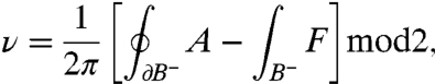
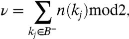
where A, F, and B- denote Berry connection, Berry curvature and half the BZ, respectively. This integration is performed on a discretized lattice in the BZ and then the  invariant ν is given by the sum of the n-field in half the 2D BZ up to modulo 2; i.e.,
 |
[2] |
where the n-field is an integer field defined at each plaquette having four discrete lattice points in the BZ as its vertices. The calculation has been done for occupied p-like bands because other occupied bands are sufficiently separated in energy. Details of the formalism can be found in refs. 23, 24, 27. The  invariants of a few QLs are given in Table 1. The films are 2D TIs or NIs depending on the thicknesses mainly due to the subband structure originated from the quantum confinement effect.
Before discussing the results of the Sb2Te3 thin film in detail, we first present some generic features of topological phase transitions. Here, we consider a phase transition by varying an external adiabatic parameter (the external electric field E⊥ perpendicular to the film in our case). A necessary condition for a topological phase transition in a 2D system is to have a gap-closing point between the topologically trivial (ν = 0) and nontrivial (ν = 1) phases. At this gap-closing point, the two fibre bundles (occupied and unoccupied bands) defined on the 2D torus (2D BZ) merge together and they exchange their topological invariants so that their topological invariants are changed after gap reopening (28). In other words, this kind of topological phase transition accompanies a (singular) gapless point to allow the change of topological invariants (which must always be integers; i.e., discrete values) under continuous deformation. The position where the gap closing occurs in the BZ is dependent on the symmetry of the system. In an inversion-symmetric system, the gap closing occurs at TRIMs (i.e., at  with
with  a reciprocal lattice vector) in the BZ, while the gap closes at points other than TRIMs in an inversion-asymmetric system (29, 30). Because we are considering thin films with external electric fields, our system corresponds to the latter case.
Now, we examine thin films of Sb2Te3 when external fields are present. 3QLs of Sb2Te3 is an example in which a phase transition occurs from a NI to a TI. As shown in Table 1, 3QLs are topologically trivial (ν = 0) when E⊥ = 0. Because Sb2Te3 is a 3D TI, it has topological surface states or Dirac cones on its surface and they are known to be at  in the BZ. In the case of thin films, there exists an interaction between the Dirac cone states at upper and lower surfaces, which opens up a small band gap at
  . Therefore, the conduction band minimum (CBM) states consist of antisymmetric states while the valence band maximum (VBM) states consist of symmetric states. When E⊥ > 0, on the other hand, the upper (lower) surface Dirac cone states shift upward (downward) in energy and the band structure shows a Rashba-like splitting pattern where two Dirac cones centered at different energy values interact to open a small gap near the Fermi energy (Fig. 2B). Here, our intention is to change the band characters of the CBM states and VBM states to drive a topological phase transition. However, a small E⊥ cannot affect the
  invariant of the system, unless a singularity or a gap-closing point is encountered (29, 30), because a topological invariant is robust under continuous deformation (it is a global property in the whole BZ). Fig. 3A shows the band structure of 3QLs with E⊥ = 0.03 V/A, and the
  invariant turns out to be 0 according to our lattice
  computation (Fig. 3E). However, if we further increase E⊥, the
  invariant becomes 1 after we pass the gap-closing point. In Fig. 3
C and F, the band structure and the n-field configuration of 3QLs with E⊥ = 0.15 V/A show that the system is now in a topologically nontrivial phase (ν = 1). The critical electric field Ec for the topological phase transition is calculated to be 0.06 < Ec < 0.075 V/A in 3QLs. On the other hand, a phase transition occurs from a TI to a NI in 4QLs of Sb2Te3. The 4QL film is in the ν = 1 phase when E⊥ = 0, but turns to the ν = 0 phase when E⊥ = 0.2 V/A. Ec is estimated to be 0.125 < Ec < 0.15 V/A in this case. To determine Ec more precisely in the
invariant becomes 1 after we pass the gap-closing point. In Fig. 3
C and F, the band structure and the n-field configuration of 3QLs with E⊥ = 0.15 V/A show that the system is now in a topologically nontrivial phase (ν = 1). The critical electric field Ec for the topological phase transition is calculated to be 0.06 < Ec < 0.075 V/A in 3QLs. On the other hand, a phase transition occurs from a TI to a NI in 4QLs of Sb2Te3. The 4QL film is in the ν = 1 phase when E⊥ = 0, but turns to the ν = 0 phase when E⊥ = 0.2 V/A. Ec is estimated to be 0.125 < Ec < 0.15 V/A in this case. To determine Ec more precisely in the  calculation, much finer k meshes are needed for convergence. Because the role of the electric fields is to “invert” the VBM and CBM states regardless of the initial band topology, the phase transition can be driven in both ways (from a NI to a TI in 3QLs and vice versa in 4QLs). We also note that 3QLs and 4QLs remain semiconducting for E⊥≦0.2 V/A although higher external fields could make the systems semimetallic.
Fig. 3.

Band structure of Sb2Te3 3QLs (A) before the topological phase transition, (B) near the gap-closing point and (C) after the phase transition. E⊥ = 0.03 V/A, E⊥ = 0.067 V/A for (A), (B), and (C), respectively. (D) The topology of 3QLs and 4QLs as E⊥ is varied. (E) The n-field configuration with E⊥ = 0.03 V/A for 3QLs. The white (black) circles denote +1 (−1). The empty plaquettes correspond to 0. The sum of the n-field in half the BZ (yellow region) is even (hence, ν = 0) in this case. (F) The n-field configuration with E⊥ = 0.15 V/A for 3QLs showing nontrivial topology (ν = 1).
The n-field configuration (Fig. 3
E and F) is gauge-dependent while the sum mod 2 in half the BZ is not, because the latter gives the  invariant of the system which is a physical quantity that should be gauge-independent. We performed the calculation using an arbitrary gauge (i.e., the one from the eigenvectors determined by the numerical diagonalization at each k point) and any other choice of the gauge should give the same
  invariant. The topological invariant obtained in the discretized BZ converges to that of the continuum when the size of the k mesh is large enough (i.e., the size of each plaquette is sufficiently small) (23, 24). The convergence of the n-field calculation is confirmed by further increasing the k mesh size and our results are also consistent with the positions of the gap-closing points and the edge state configurations.
The band topology of a 2D system can also be identified by investigating the dispersion of edge states. A 2D TI has topologically protected edge states characterized by the fact that they cross the Fermi level at an odd number of points in half the BZ; i.e., they connect the conduction bulk states and valence bulk states. The topological edge states are robust against local disorder (they remain gapless due to the Kramer’s degeneracy and cannot be localized due to the absence of backscattering) as long as the time-reversal symmetry is maintained. In contrast, a 2D NI has topologically trivial edge states that cross the Fermi level an even number of times in half the BZ. The edge states can be localized and a gap might open if some disorder is present (4, 12, 31).
To depict the dispersion of electronic states at the edge of Sb2Te3 thin films, we first construct a tight-binding Hamiltonian with maximally localized Wannier functions (MLWFs) from the results of the first-principles calculation (32, 33). Then the Green’s functions are obtained using a highly convergent iterative method and we calculate the local density of states (LDOS) for both the edge principal layer and the bulk principal layer from them (25, 26). This method is employed to describe an edge of the semiinfinite 2D system and it provides the clear connectivity between the edge states and the bulk states. In Fig. 4A, the LDOS of the edge principal layer in 3QLs of Sb2Te3 is given, and it shows no edge states near the 2D bulk energy gap. On the contrary, for 3QLs with E⊥ = 0.15 V/A, there exist topological gapless edge states that connect the bulk valence and conduction regions constituting a “one-dimensional (1D) Dirac cone” centered at  (Fig. 4B). Even though the specific edge dispersion is dependent on the atomic configuration at the edge, the number of crosses at the Fermi level (modulo 2) does not change because it is determined by the
  invariant of the (2D) bulk band structure. For comparison, we present the LDOS for a bulk principal layer in this case (Fig. 4C), which shows that the gapless states in Fig. 4B are indeed the edge states. These configurations of edge states are consistent with the lattice computations of the
  invariants in view of the bulk-boundary correspondence. In the case of 4QLs, there is one (two) edge state in half the 1D BZ before (after) the phase transition.
Fig. 4.

LDOS of the edge principal layer in 3QLs of Sb2Te3 with (A) E⊥ = 0.0 V/A and (B) E⊥ = 0.15 V/A. (C) LDOS of the bulk principal layer in 3QLs with E⊥ = 0.15 V/A to compare with (B). Topological edge states or a “1D Dirac cone” [guided by the black dotted line in (B)] is present at  in the topologically nontrivial phase.
The value of Ec depends on the system. In 2QLs of Sb2Te3, the gap size is relatively large and the phase transition does not occur up to E⊥ = 0.4 V/A. If we want to utilize this type of phase transition as an on/off switch of topologically robust edge states, it is crucial to increase the gap size for stability of operation but, at the same time, decrease Ec for practicality. Thus, various types of materials and other external parameters (stress, etc.) should be considered as well to find an optimal system. In contrast, if we want a material whose band topology must not be changed easily (say, by the influence of the substrate potential in experiment), a large value of Ec would be desirable.
Conclusion
In conclusion, we have shown that topological quantum phase transitions occur under external electric fields in thin films of Sb2Te3. Particularly, 3QLs and 4QLs are predicted to have moderate values of the critical electric field for the phase transition. As the field strength increases, the 3QLs film shows a transition from a NI to a TI while the 4QLs film shows one from a TI to a NI. The edge state configurations are confirmed to be consistent with the bulk topology in accordance with the bulk-boundary correspondence, and a single 1D Dirac cone appears in the case of 3QLs after the phase transition. This type of the topological phase transition might be useful for practical control of the topologically robust conducting channels at the edges.
Materials and Methods
Electronic structures were obtained using first-principles calculations based on the PBE-type (34) generalized gradient approximation to the density functional theory as implemented in the Quantum-Espresso package (35). We employed fully relativistic pseudopotentials including spin-orbit coupling and a plane-wave basis with the cutoff energy of 34 Ry. For the atomic structure, experimental bulk lattice constant was used (36). We dealt with thin films of Sb2Te3 in the supercell slab geometry with sufficient vacuum regions (for example, 20 Å in the case of 3 QLs) to avoid the spurious (unwanted) electrostatic interactions between periodic images. Band structures were confirmed to be converged with respect to the vacuum size. The external electric field was described by a saw-tooth-like potential in the Hamiltonian. The lattice computation of the  invariant was done using the wave functions on a discretized BZ. Also, for the edge state dispersion, Wannier90 package was partly used to calculate the edge Green’s function in terms of MLWFs (37).
Acknowledgments.
M.K. thanks C. Park, H. Jeong, and H. J. Choi for fruitful discussions and comments. This work was supported by the National Research Foundation (NRF) of Korea, grant funded by the Korea government Ministry of Education, Science and Technology (MEST) No.2006-0093853. Computations were performed through the support of Korea Institute of Science and Technology Information (KISTI).
Footnotes
The authors declare no conflict of interest.
References
- 1.Klitzing Kv, Dorda G, Pepper M. New method for high-accuracy determination of the fine-structure constant based on quantized Hall resistance. Phys Rev Lett. 1980;45:494–497. [Google Scholar]
- 2.Thouless DJ, Kohmoto M, Nightingale MP, den Nijs M. Quantized Hall conductance in a two-dimensional periodic potential. Phys Rev Lett. 1982;49:405–408. [Google Scholar]
-
3.Kane CL, Mele EJ.
 topological order and the quantum spin Hall effect. Phys Rev Lett. 2005;95:146802. doi: 10.1103/PhysRevLett.95.146802. [DOI] [PubMed] [Google Scholar]
 - 4.Kane CL, Mele KJ. Quantum spin Hall effect in graphene. Phys Rev Lett. 2005;95:226801. doi: 10.1103/PhysRevLett.95.226801. [DOI] [PubMed] [Google Scholar]
- 5.Bernevig BA, Hughes TL, Zhang S-C. Quantum spin Hall effect and topological phase transition in HgTe quantum wells. Science. 2006;314:1757–1761. doi: 10.1126/science.1133734. [DOI] [PubMed] [Google Scholar]
- 6.König M, et al. Quantum spin Hall insulator state in HgTe quantum wells. Science. 2007;318:766–770. doi: 10.1126/science.1148047. [DOI] [PubMed] [Google Scholar]
- 7.Fu L, Kane CL, Mele EJ. Topological insulators in three dimensions. Phys Rev Lett. 2007;98:106803. doi: 10.1103/PhysRevLett.98.106803. [DOI] [PubMed] [Google Scholar]
- 8.Fu L, Kane CL. Topological insulators with inversion symmetry. Phys Rev B. 2007;76:045302. [Google Scholar]
- 9.Zhang HJ, et al. Electronic structures and surface states of the topological insulator Bi1-xSbx. Phys Rev B. 2009;80:085307. [Google Scholar]
- 10.Qi X-L, Hughes TL, Zhang S-C. Topological field theory of time-reversal invariant insulators. Phys Rev B. 2008;78:195424. [Google Scholar]
- 11.Hsieh D, et al. A topological Dirac insulator in a quantum spin Hall phase. Nature. 2008;452:970–975. doi: 10.1038/nature06843. [DOI] [PubMed] [Google Scholar]
- 12.Hasan MZ, Kane CL. Colloquium: topological insulators. Rev Mod Phys. 2010;82:3045–3067. [Google Scholar]
- 13.Zhang H, Liu C-X, Qi X-L, Fang Z, Zhang S-C. Topological insulators in Bi2Se3, Bi2Te3 and Sb2Te3 with a single Dirac cone on the surface. Nat Phys. 2009;5:438–442. [Google Scholar]
- 14.Jin H, Song J-H, Freeman AJ, Kanatzidis MG. Candidates for topological insulators: Pb-based chalcogenide series. Phys Rev B. 2011;83:041202. (R) [Google Scholar]
- 15.Yan B, Liu C-X, Zhang H-J, Yam C-Y, Qi X-L. Theoretical prediction of topological insulators in thallium-based III-V-VI2 ternary chalcogenides. Europhys Lett. 2010;90:37002. [Google Scholar]
- 16.Smith JC, Banerjee S, Pardo V, Pickett WE. Dirac point degenerate with massive bands at a topological quantum critical point. Phys Rev Lett. 2011;106:056401. doi: 10.1103/PhysRevLett.106.056401. [DOI] [PubMed] [Google Scholar]
- 17.Shan W-Y, Lu H-Z, Shen S-Q. Effective continuous model for surface states and thin films of three-dimensional topological insulators. New J Phys. 2010;12:043048. [Google Scholar]
- 18.Li H, Sheng L, Sheng DN, Xing DY. Chern number of thin films of the topological insulator Bi2Se3. Phys Rev B. 2010;82:165104. [Google Scholar]
- 19.Li J, Chang K. Electric field driven quantum phase transition between band insulator and topological insulator. Appl Phys Lett. 2009;95:222110. [Google Scholar]
- 20.Liu C-X, et al. Oscillatory crossover from two-dimensional to three-dimensional topological insulators. Phys Rev B. 2010;81:041307. (R) [Google Scholar]
- 21.Zhang Y, et al. Crossover of the three-dimensional topological insulator Bi2Se3 to the two-dimensional limit. Nat Phys. 2010;6:584–588. [Google Scholar]
- 22.Fu L, Kane CL. Time reversal polarization and a Z2 adiabatic spin pump. Phys Rev B. 2006;74:195312. [Google Scholar]
- 23.Fukui T, Hatsugai Y. Quantum spin Hall effect in three dimensional materials: lattice computation of Z2 topological invariants and its application to Bi and Sb. J Phys Soc Jpn. 2007;76:053702. [Google Scholar]
- 24.Fukui T, Hatsugai Y, Suzuki H. Chern numbers in discretized Brillouin zone: efficient method of computing (spin) Hall conductances. J Phys Soc Jpn. 2005;74:1674–1677. [Google Scholar]
- 25.Sancho MPL, Sancho JML, Rubio J. Quick iterative scheme for the calculation of transfer matrices: application to Mo(100) J Phys F Met Phys. 1984;14:1205–1215. [Google Scholar]
- 26.Sancho MPL, Sancho JML, Rubio J. Highly convergent schemes for the calculation of bulk and surface Green functions. J Phys F Met Phys. 1985;15:851–858. [Google Scholar]
- 27.Xiao D, et al. Half-Heusler compounds as a new class of three-dimensional topological insulators. Phys Rev Lett. 2010;105:096404. doi: 10.1103/PhysRevLett.105.096404. [DOI] [PubMed] [Google Scholar]
- 28.Moore JE, Balents L. Topological invariants of time-reversal-invariant band structures. Phys Rev B. 2007;75:121306. (R) [Google Scholar]
- 29.Murakami S, Iso S, Avishai Y, Onoda M, Nagaosa N. Tuning phase transition between quantum spin Hall and ordinary insulating phases. Phys Rev B. 2007;76:205304. [Google Scholar]
- 30.Murakami S, Kuga S-i. Universal phase diagrams for the quantum spin Hall systems. Phys Rev B. 2008;78:165313. [Google Scholar]
- 31.Zhang S-c. Topological states of quantum matter. Physics. 2008;1:6. doi: 10.1103/Physics.1.6. [Google Scholar]
- 32.Marzari N, Vanderbilt D. Maximally localized generalized Wannier functions for composite energy bands. Phys Rev B. 1997;56:12847–12865. [Google Scholar]
- 33.Souza I, Marzari N, Vanderbilt D. Maximally localized Wannier functions for entangled energy bands. Phys Rev B. 2001;65:035109. [Google Scholar]
- 34.Perdew JP, Burke K, Ernzerhof M. Generalized gradient approximation made simple. Phys Rev Lett. 1996;77:3865–3868. doi: 10.1103/PhysRevLett.77.3865. [DOI] [PubMed] [Google Scholar]
- 35.Giannozzi P, et al. QUANTUM ESPRESSO: a modular and open-source software profect for quantum simulations of materials. J Phys-Condens Mat. 2009;21:395502. doi: 10.1088/0953-8984/21/39/395502. [DOI] [PubMed] [Google Scholar]
- 36.Thonhauser T, Scheidemantel TJ, Sofo JO, Badding JV, Mahan GD. Thermoelectric properties of Sb2Te3 under pressure and uniaxial stress. Phys Rev B. 2003;68:085201. [Google Scholar]
- 37.Mostofi AA, et al. wannier90: a tool for obtaining maximally-localized Wannier functions. Computer Physics Communications. 2008;178:685–699. [Google Scholar]