Abstract
We study two-terminal devices for DNA sequencing which consist of a metallic graphene nanoribbon with zigzag edges (ZGNR) and a nanopore in its interior through which the DNA molecule is translocated. Using the nonequilibrium Green functions combined with density functional theory, we demonstrate that each of the four DNA nucleobases inserted into the nanopore, whose edge carbon atoms are passivated by either hydrogen or nitrogen, will lead to a unique change in the device conductance. Unlike other recent biosensors based on transverse electronic transport through translocated DNA, which utilize small (of the order of pA) tunneling current across a nanogap or a nanopore yielding a poor signal-to-noise ratio, our device concept relies on the fact that in ZGNRs local current density is peaked around the edges so that drilling a nanopore away from the edges will not diminish the conductance. Inserting a nucleobase into the nanopore affects the charge density in the surrounding area, thereby modulating edge conduction currents whose magnitude is of the order of μA at bias voltage ≃ 0.1 V. The proposed biosensors are not limited to ZGNRs and they could be realized with other nanowires supporting transverse edge currents, such as chiral GNRs or wires made of two-dimensional topological insulators.
The successful realization of fast and low-cost methods for reading the sequence of DNA bases is envisaged to lead to personalized medicine and applications in various subfields of genetics. Solid-state nanopores1,2 represent one of the pillars of the so-called third generation sequencing.3 The key issues in this approach revolve around how to slow down the translocation speed of DNA and how to achieve single-base resolution.
Very recent experiments 4–6 on DNA translocation through graphene nanopores have introduced a new contender into this arena. Graphene—the recently discovered7 two-dimensional allotrope of carbon whose atoms are densely packed into a honeycomb lattice—brings its unique electronic and mechanical properties into the search for an optimal nanoelectronic biosensor. Since single layer graphene is only one-atom-thick, the entire thickness of the nanopore through which DNA is threaded is comparable to the dimensions of DNA nucleotides. Therefore, there is only one recognition point rather than multiple contacts with DNA in the nanopore.
However, the recent experiments4–6 on nanopores within single or multilayer large-area graphene, which have measured fluctuations in the vertical ionic current flow due to DNA translocation through the pore, have not reached sufficient resolution to detect and identify individual nucleobases. An alternative scheme is to adapt the transverse current approach to graphene-based biosensors.8–11 The past several years have seen a number of theoretical proposals12–16 and experiments17,18 on nanogaps between two metallic electrodes (typically gold 12–14 or carbon nanotubes15,16) where the longitudinally translocated DNA through the gap modulates the transverse tunneling current. Also, recent first-principles simulations have analyzed modulation of the tunneling current for a nanogap9,10 between metallic GNRs with zigzag edges (ZGNR) or a nanopore11 within semiconducting graphene nanoribbons with armchair edges (AGNR).
However, the tunneling-current based graphene biosensors will face the same challenges15 encountered by current experimental efforts to utilize transverse tunneling current across a gap between two gold electrodes,17,18 such as poor signal-to-noise ratio at small bias voltages due to the fact that molecular eigenlevels are typically far away from the Fermi energy of the electrodes. In this case, the tunneling is off-resonant and currents are of the order of pA at typically applied17,18 bias voltage ≃ 0.5 V. Such small off-resonant tunneling currents are highly dependent on difficult-to-control relative geometry between the molecule and electrodes, so that recent experiments have measured broad current distributions corresponding to each nucleotide in the case of bare gold electrodes17 and somewhat narrower but still overlapping distributions18 for functionalized gold electrodes.
Similarly, first-principles simulations9 of tunneling through the nanogap hosting a DNA nucleotide between two metallic GNRs have revealed current variation over several orders of magnitude (e.g., 10−2–10−10 nA at bias voltage9 1 V) when changing the position and orientation of nucleotides within the gap. These simulations have also revealed a major drawback for using graphene electrodes in conventional tunneling-current based biosensors where several10 physical mechanisms conspire to reduce their conductance far below those utilizing gold nanoelectrodes.17,18
The theoretical proposals to increase the transverse current across the nanogap in vacuum, as in the case of carbon nanotube (CNT) electrodes terminated with nitrogen15 or close-ended CNT electrodes separated by an ultra-short gap,16 offer only moderate improvement (~ 1–10 nA currents at ≃ 0.5 V bias voltage 15,16). Applying higher bias voltage to increase the current signal is detrimental since it can lead to attraction of the negatively charged DNA backbone toward one of the electrodes thereby impeding the translocation, or even a breakdown of the electrodes or the substrate at sufficiently high electric fields.
Here we propose a novel device concept that could resolve these issues by abandoning the usage of small tunneling current altogether. Its operation crucially relies on the existence of metallic nanowires in which the spatial current profile22 is confined around their transverse edges, so that drilling a nanopore should not change significantly their conductance which is of the order of few conductance quanta 2e2/h. When one of the four nucleobases of DNA—adenine (A), cytosine (C), guanine (G), or thiamine (T)—is inserted into the nanopore in the course of DNA translocation, it will affect the charge density around the pore thereby modulating edge conduction currents that are several orders of magnitude larger than tunneling currents across nanogaps8–10,12,17,18 or nanopores in AGNRs11 (where edge currents are absent). The large operating current may also remove the need to slow down or constrain the DNA molecule as it translocates, since the measurement speed may be high enough to prevent Brownian fluctuations of the molecule from blurring the signal.
The candidate nanowires supporting edge currents can be found among GNRs with zigzag edges or the very recently fabricated23 chiral GNRs, as well as among two-dimensional topological insulators (2D TI).24 In the case of zigzag or chiral GNRs, spatial profile of local currents carried by electrons around the charge neutral point (CNP) shows large magnitude around the edge25 and a tiny current flowing through their interior. In 2D TI nanowires, similar situation will appear if the wire is narrow enough so that helical edge states overlap slightly and edge currents can be modulated. Otherwise, in sufficiently wide 2D TI wires current is strictly confined to the edges and cannot be affected by time-reversal-preserving impurities, vacancies or modulation of charge density because of the fact that helical edge states guide electrons of opposite spin in opposite directions to prevent their backscattering.24 We note that recent first-principles analysis has suggested that GNRs could also be converted into 2D TI wires via heavy adatom deposition in order to increase the spin-orbit coupling.26
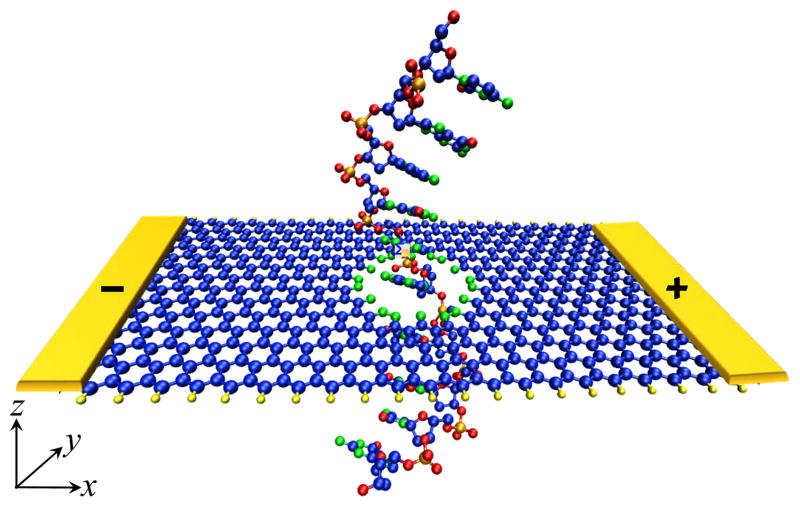
The recent proliferation of nanofabrication techniques23,27,28 for GNRs with ultrasmooth edges is making them widely available, and their exposed surface allows for an easier integration into biosensors. Therefore, in the device depicted in Figure 1 we choose to consider a GNR with zigzag edges. Note that edge currents in ZGNRs have already been confirmed in experiments where they were exploited to increase heat dissipation around edge defects and, thereby, rearrange atomic structure locally until sharply defined zigzag edge is achieved.28
Figure 1.
Schematic view of the proposed two-terminal device where transverse conduction current flows around the zigzag edges of a metallic graphene nanoribbon with a nanopore, while DNA molecule is translocated through the pore to induce nucleobase-specific-modulation of such edge currents. The active device region, which is simulated via first-principles quantum transport formalism, consists of a segment of 14-ZGNR (composed of 14-zigzag chains which determine its width ≈3.1 nm) and a nanopore of ≈ 1.2 nm diameter. The edge carbon atoms of the nanopore are passivated by either hydrogen or nitrogen, while edge atoms of ZGNR itself are passivated by hydrogen. The total number of simulated atoms (C-blue, H-yellow, N-green, O-red, P-orange) in the active region, including the nucleobase within the nanopore, is around 700.
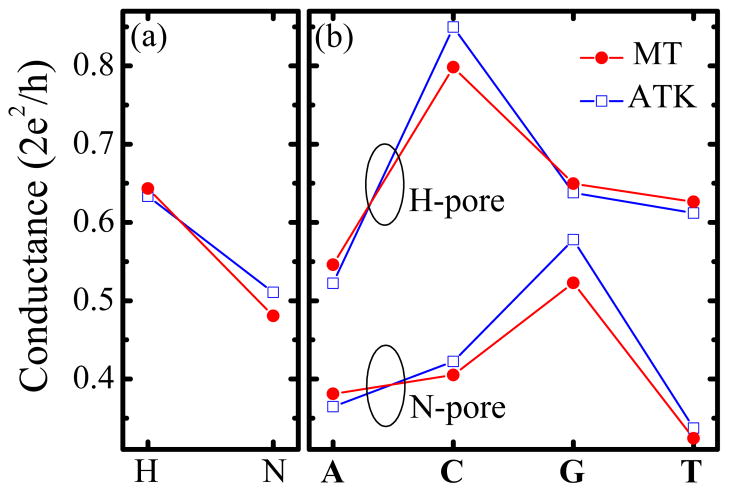
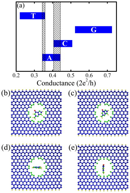
The ZGNR-based device corroborates the general modulation-of-edge-currents concept discussed above, as demonstrated by our central result in Figure 2 obtained via first-principles quantum transport simulations using two completely different19–21 computational implementations of the nonequilibrium Green function coupled to density functional theory (NEGF-DFT) formalism.29–31 Figure 2 shows how each nucleobase inserted into the center of the nanopore [within the yz-plane, see Figure 3(e)] will change the device room-temperature conductance by a specific amount. When spatial orientation of nucleobases with respect to the pore is changed as in Figure 3(b)–(d), the conductance will vary within the intervals shown in Figure 3(a). The DNA base-specific modulation of current I is achieved while remaining in the linear-response regime, where I = GV is of the order of μA at bias voltage ≃ 0.1 V. Such sizable operating current is expected to be much larger than electronic noise caused13,14 by ionic currents and structure fluctuations of DNA during the translocation process.
Figure 2.
(a) The room-temperature conductance of the two-terminal 14-ZGNRs with ≈ 1.2 nm diameter nanopore whose edge carbon atoms are passivated by either hydrogen (H-pore) or nitrogen (N-pore). (b) The room-temperature conductance of the same device as in panel (a) when one of the four nucleobases (A-adenine, C-cytosine, G-guanine, T-thymine) is inserted into the center of the nanopore within the yz-plane [Figure 3(e)]. These conductances are computed via first-principles quantum transport simulations where both panels compare results obtained using two different NEGF-DFT codes—our home-grown MT-NEGF-DFT19,20 and commercial ATK.21
Figure 3.
(a) The variation of the room-temperature conductance of 14-ZGNR with N-pore due to the rotation of A, C, G, T nucleobases within the nanopore. The shaded vertical rectangles mark the regions of overlap between the conductance intervals associated with different nucleobases. The specific positions of a nucleobase (guanine in the example) within the N-pore that define the conductance intervals shown in panel (a) are illustrated in [see coordinate system in Figure 1]: (b) nucleobase within the xy-plane (hosting also ZGNR and nanopore); (c) nucleobase within the plane inclined at an angle of 45° with respect to the xy-plane; (d) nucleobase within the xz-plane; (e) nucleobase within the yz-plane. The conductances in panel (a) were computed using our homegrown MT-NEGF-DFT code.19,20
In the NEGF-DFT formalism,29–31 the Hamiltonian is not known in advance and has to be computed by finding the converged spatial profile of charge via the self-consistent DFT loop for the density matrix whose diagonal elements give charge density.31 The NEGF formalism for steady-state transport operates with two central quantities, retarded G(E) and lesser Green functions G<(E), which describe the density of available quantum states and how electrons occupy those states, respectively. In the coherent transport regime (i.e., in the absence of electron-phonon or electron-electron dephasing processes), only the retarded Green function is required to post-process the result of the DFT loop by expressing the zero-bias electron transmission function between the left (L) and the right (R) electrodes as:
 |
(1) |
The matrices account for the level broadening due to the coupling to the electrodes, where ΣL,R(E) are the self-energies introduced by the ZGNR electrodes.31 The retarded Green function matrix of the active device region is given by G = [ES − H − ΣL − ΣR] −1, where in the local orbital basis {φi} Hamiltonian matrix H is composed of elements Hij = 〈 φi|ĤKS |φj〉 and ĤKS is the effective Kohn-Sham Hamiltonian obtained from the DFT self-consistent loop. The overlap matrix S has elements Sij = 〈 φi|φj〉.
The conductance at finite temperature T is obtained from the transmission function
 (E) using the standard Landauer formula for two-terminal devices
 |
(2) |
where f(E) = {1 + exp[(E − μ)/kBT]}−1 is the Fermi function of the macroscopic reservoirs into which semi-infinite ideal leads terminate. The electrochemical potential μ is the same for both reservoirs at vanishingly small bias voltage.
The retarded Green function G is computed for the active region of the biosensor shown in Figure 1 consisting of around 700 atoms. This active region is attached to two semi-infinite ZGNRs electrodes of the same width. Whereas graphene is mechanically strong, it can be used as both the membrane material carrying a nanopore and the electrode material. In real devices, ZGNR electrodes will eventually need to be connected to metallic electrodes attached to an external battery. However, the fact that GNRs used in experiments are typically rather long and screening takes place over a distance much shorter31 than the active region justifies the use of semi-infinite ZGNRs as two electrodes in our simulations.
The edge carbon atoms will catch any bond partner they can possibly get to saturate their dangling bonds. We assume that ZGNR edges are passivated by hydrogen, while edge atoms of the nanopore can be bonded covalently to either hydrogen (H-pore) or nitrogen (N-pore). Prior to transport calculations, we use DFT to relax the coordinates of all atoms within finite-ZGNR+nanopore or finite-ZGNR+nanopore+nucleobase until the forces on individual atoms are minimized to be smaller than 0.05 eV/Å2. The converged result of this procedure is illustrated in Figure 3(b)–(d) which shows how carbon and hydrogen atoms around the nanopore move away from it so that the edge of ZGNR acquires a slight curvature.
The early theoretical studies of ZGNR-based devices have utilized a simplistic tight-binding model32 with single π orbital per site and nearest neighbor hopping only, or its long-wavelength (continuum) approximation—the Dirac-Weyl Hamiltonian33—valid close to CNP. However, making connections to realistic device applications requires taking into account charge transfer31 between different atoms34 that can be used to passivate edges or chemically functionalize graphene, as well as the charge redistribution31 when finite bias voltage is applied. For example, the tight-binding model with the nearest-neighbor hopping predicts22,32 incorrectly that zero-temperature conductance of an infinite homogeneous ZGNR is G = 2e2/h around the CNP and that current density profile is peaked22 in the middle of ZGNR despite local density of states reaching maximum around the edges.
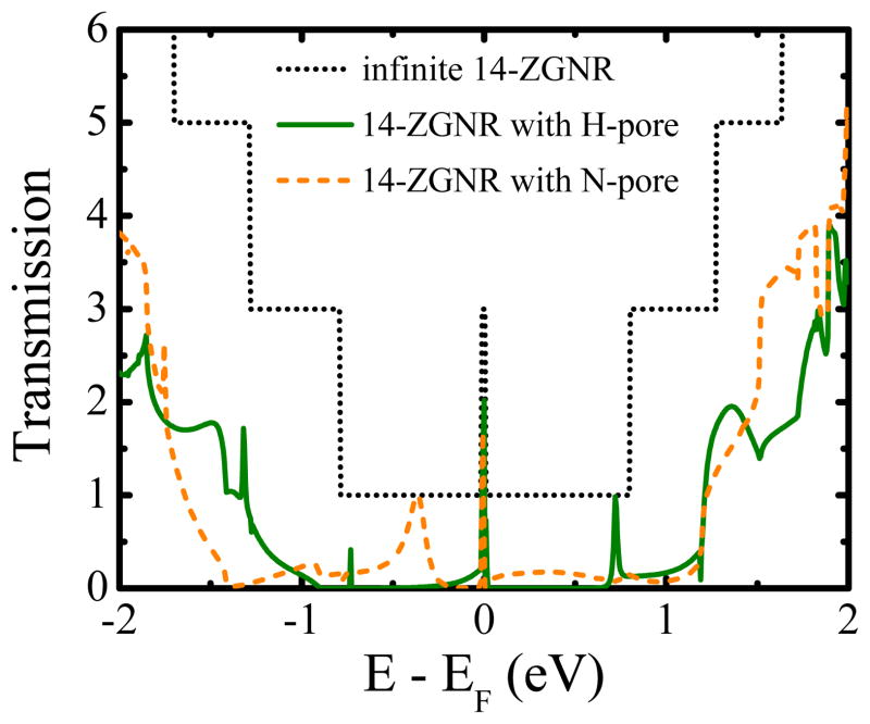
On the other hand, first-principles methods find that the zero-temperature conductance of an infinite homogeneous ZGNR is G = 6e2/h around the CNP while local current is confined to flow mostly around the zigzag edges.25 This is illustrated by quantized steps in the transmission function in Figure 4 where
 = 3 around the Fermi energy E − EF = 0, and the zero-temperature conductance is given by the simplified version of Eq. (2),
![]() . In the absence of any nucleobase, the transmission function
. In the absence of any nucleobase, the transmission function
 (E) plotted in Figure 4 remains large
 ≃ 2 around CNP E − EF = 0 for an infinite ZGNR with either H-pore or N-pore. This finding confirms our conjecture that a nanopore in the interior of a ZGNR is not able to substantially modify the current flow inherited from a homogeneous nanoribbon since the local current density is mostly confined around the edges for electrons injected at energies sufficiently close to CNP (E − EF = 0). We note that using spin-unrestricted DFT reveals the presence of edge magnetic ordering and the corresponding band gap opening in ZGNRs which, however, is easily destroyed at room temperature35,36 so that for realistic device operation ZGNRs can be considered to be metallic.36
Figure 4.
The zero-bias electronic transmission function Eq. (1) for an infinite homogeneous 14-ZGNR, whose edge carbon atoms are passivated by hydrogen, and the same nanoribbon with empty H-pore or N-pore of diameter ≈ 1.2 nm (see Figure 1) drilled in its interior.
The change in the room-temperature conductance of empty nanopores in Figure 2(a) and nanopores with inserted nucleobase in Figure 2(b) is more pronounced when the pore is terminated with nitrogen. Since reliability of predictions of NEGF-DFT simulations requires careful selection of the basis set and pseudopotentials in the DFT part of the calculation,37 Figure 2 plots conductances obtained using two different computational implementations of the NEGF-DFT formalism. Our home-grown MT-NEGF-DFT code19,20 utilizes ultrasoft pseudopotentials and Perdew-Burke-Ernzerhof (PBE) parametrization of the generalized gradient approximation (GGA) for exchange-correlation functional of DFT. The localized basis set is constructed from atom-centered orbitals (six per C atom, four per H atom, 8 per N atom, and 8 per O atom) that are optimized variationally (atomic radius 8.0 Bohr) for the electrodes and the active region separately while their electronic structure is obtained concurrently. For comparison, we also used commercial ATK code21 where pseudoatomic local orbitals are single-zeta polarized on C and H atoms and double-zeta polarized on N and O atoms (as well as on P atoms in the Supporting Information). In the case of ATK, we use Troullier-Martins norm-conserving pseudopotentials, Perdew-Zunger (PZ) parametrization of the local density approximation (LDA) for the exchange-correlation functional of DFT, and energy mesh cutoff for the real-space grid is 65.0 Hartree. Figure 2 emphasizes that both first-principles quantum transport simulations yield very similar results for the conductance.
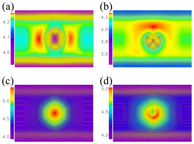
To explain the mechanisms by which nucleobases modulate charge transport in a ZGNR with a nanopore, we plot in Figure 5 the self-consistent Hartree potential within the central region of our biosensor at zero bias voltage obtained by solving the Poisson equation with the boundary conditions that match the electrostatic potentials of two attached ZGNR electrodes. We see that there is a substantial difference in this potential when switching from an empty pore to a nanopore containing a nucleobase. In the examples in Figure 5, cytosine is inserted into the H-pore and thymine into the N-pore—these are the situations for which there is the largest change in conductance in Figure 2 when compared to the corresponding empty nanopores.
Figure 5.
The self-consistent Hartree potential at zero bias voltage for the active region of 14-ZGNR biosensors (Figure 1) with: (a) empty H-pore; (b) H-pore with cytosine positioned in its center within the yz-plane [Figure 3(e)]; (c) empty N-pore; and (d) N-pore with thymine positioned in its center within the yz-plane [Figure 3(e)].
An important issue9,11 for the uniqueness of the conductance modulation signal associated with each nucleobase is to examine how such signal gets modified when varying the orientation of DNA bases with respect to the nanopore. For selected orientations shown in Figure 3(b)–(e), the conductance variations for all four nucleobases are plotted in Figure 3(a). We find small overlap between conductance distribution for T and A or A and C, and no overlap between conductance intervals for T and C or C and G. Nevertheless, the intervals in Figure 3(a) should be considered as setting only the limits on conductance variation since not all values within the interval will be sampled experimentally. In other words, some of the nucleobase positions in Figure 3(b)–(e) are selected to generate maximum conductance variation, and they would require significant bending of the DNA molecule to put the nucleobase into such position with respect to the nanopore.
The operation of a realistic biosensor will involve a substrate underneath (typically SiO2 or Si3N4, unless the ribbon is partially suspended across a small slit in the substrate while still separating two solution chambers), a solvent, DNA counterions13 and, perhaps most important, fluctuations in the structure of DNA. These effects were not taken into account in our proof-of-concept calculations. While time-dependent simulations to capture these effects within fully quantum transport framework are far beyond present capabilities of NEGF-DFT codes, using molecular dynamics (MD) simulations38 to obtain snapshots of translocated DNA within the pore in the presence of solvent and substrate makes it possible to feed10,13,14,16 real-time atomic coordinates (of the nucleobases, water39 and ions) into NEGF-DFT methodology, which is something we leave for future investigation.
Also, phosphate and sugar groups comprising the DNA backbone will be adjacent to the nucleobase within the nanopore and could affect the modulation of edge currents. Nevertheless, we anticipate that most of additional factors will manifest only as the small noise on the top of large operating current in our device. We confirm this by examining some of the secondary effects in additional Figures provided as Supporting Information which show changes in the conductance of the ZGNR+N-pore biosensor when: (i) isolated sugar or phosphate group is inserted in the nanopore (Figure S1); (ii) nucleobases are attached to sugar-phosphate backbone (Figure S2); and (iii) nucleobase is translated vertically above or below the nanopore (Figure S3). In all three cases, the conductance change is small (≲ 10%) and certainly enclosed by the intervals delineated in Figure 3(a).
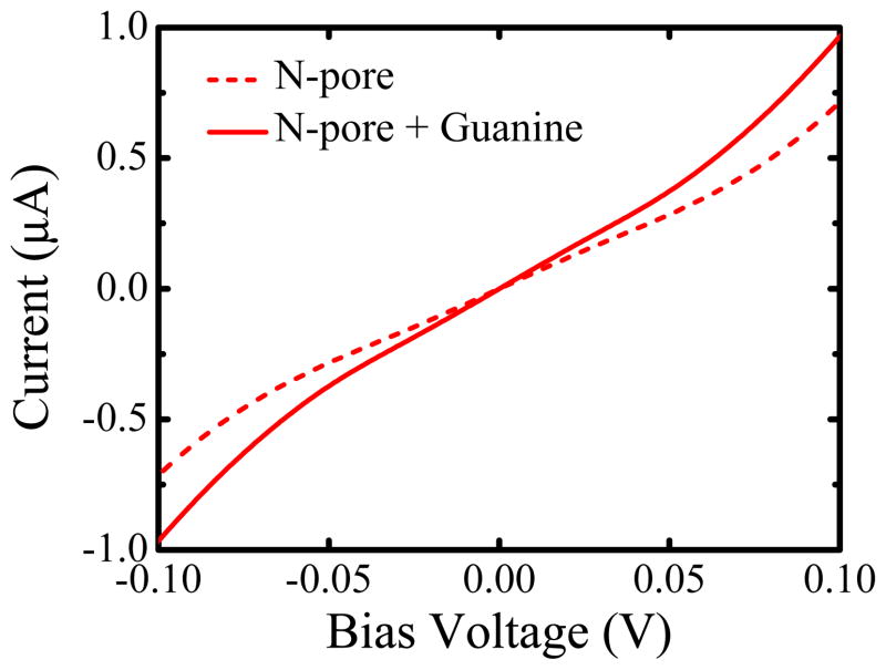
Finally, in Figure 6 we clarify the range of operating bias voltages that ensures a linear-response regime for our biosensor, where the measured current is given simply by multiplying conductances in Figure 2 and Figure 3 by the bias voltage. Both current-voltage characteristics in Figure 6, computed for a biosensor with an empty N-pore and the same pore containing guanine, behave linearly within the interval ≃ −0.05 V to ≃ 0.05 V.
Figure 6.
Current-voltage characteristics of 14-ZGNR with N-pore which is empty (dashed line) or contains guanine (solid line) in its center placed within the yz-plane [Figure 3(e)]. The current at finite bias voltage is computed using our home-grown MT-NEGF-DFT code.19,20
In conclusion, using first-principles quantum transport simulations, we investigated a novel type of graphene nanopore-based sensors for rapid DNA sequencing which rely on DNA base-specific modulation of a large transverse conduction current (of the order of μA at bias voltage ≃ 0.1 V). This is achieved by exploiting unique features of the electronic transport through graphene nanoribbons with zigzag edges where local current density is confined mostly around the nanoribbon edges. Other candidate nanowires that carry edge currents are the recently fabricated23 chiral GNRs. The nanopore in the GNR interior cannot substantially diminish the edge currents, whose magnitude is then modulated by the passage of nucleobases in the course of DNA translocation through the pore. Our analysis demonstrates that each DNA base will generate a unique modulation of the charge density and the corresponding electrostatic potential in the surrounding area. The operating current, which is several orders of magnitude greater than the tunneling current employed in previously considered biosensors with transverse electron transport8–18 is expected to be much larger than its fluctuations due to thermal vibrations of the graphene membrane, structural fluctuations of the translocated DNA molecule and dynamical environment (counterions and water molecules) influence on the electronic structure of nucleotides in solution. The device remains in the linear-response regime for bias voltages ≲ 0.05 V. We also anticipate that the large ~ 1 μA operating current should allow measurements of conductance fluctuations with off-the-shelf amplifiers at a rate commensurate with DNA translocation, possibly removing the need to slow down or constrain the DNA molecule as it translocates.
Supplementary Material
Acknowledgments
We thank V. Meunier, S. Sanvito and R. H. Scheicher for illuminating discussions and valuable suggestions. This work was supported by DOE Grant No. DE-FG02-07ER46374 (K. K. S. and B. K. N.) and NIH Grants No. R21HG004767 and and R21HG006313 (M. D.). The supercomputing time was provided in part by the NSF through TeraGrid resource TACC Ranger under Grant No. TG-DMR100002.
Footnotes
Supporting Information Available
Three additional figures are presented which show the effect of sugar-phosphate backbone, or translation of a nucleobase above and below the nanopore, on the transverse edge currents in ZGNR with N-pore devices. This material is available free of charge via the Internet at http://pubs.acs.org.
References
- 1.Venkatesan BM, Bashir R. Nature Nanotechnology. 2011;6:615. doi: 10.1038/nnano.2011.129. [DOI] [PubMed] [Google Scholar]
- 2.Healy K, Schiedt B, Morrison AP. Nanomedicine. 2007;2:875. doi: 10.2217/17435889.2.6.875. [DOI] [PubMed] [Google Scholar]
- 3.Schadt EE, Turner S, Kasarskis A. Human Molecular Genetics. 2010;19:R227. doi: 10.1093/hmg/ddq416. [DOI] [PubMed] [Google Scholar]
- 4.Merchant CA, Healy K, Wanunu M, Ray V, Peterman N, Bartel J, Fischbein MD, Venta K, Luo Z, Johnson ATC, Drndić M. Nano Letters. 2010;10:2915–2921. doi: 10.1021/nl101046t. [DOI] [PubMed] [Google Scholar]
- 5.Schneider GF, Kowalczyk SW, Calado VE, Pandraud G, Zandbergen HW, Van-dersypen LMK, Dekker C. Nano Letters. 2010;10:3163–3167. doi: 10.1021/nl102069z. [DOI] [PubMed] [Google Scholar]
- 6.Garaj S, Hubbard W, Reina A, Kong J, Branton D, Golovchenko JA. Nature. 2010;467:190–193. doi: 10.1038/nature09379. [DOI] [PMC free article] [PubMed] [Google Scholar]
- 7.Geim AK. Science. 2009;324:1530–1534. doi: 10.1126/science.1158877. [DOI] [PubMed] [Google Scholar]
- 8.Postma HWC. Nano Lett. 2010;10:420. doi: 10.1021/nl9029237. [DOI] [PubMed] [Google Scholar]
- 9.Prasongkit J, Grigoriev A, Pathak B, Ahuja R, Scheicher RH. Nano Lett. 2011;11:1941–1945. doi: 10.1021/nl200147x. [DOI] [PubMed] [Google Scholar]
- 10.He Y, Scheicher RH, Grigoriev A, Ahuja R, Long S, Huo Z, Liu M. Advanced Functional Materials. 2011;21:2674. [Google Scholar]
- 11.Nelson T, Zhang B, Prezhdo OV. Nano Lett. 2010;10:3237. doi: 10.1021/nl9035934. [DOI] [PubMed] [Google Scholar]
- 12.Zwolak M, Di Ventra M. Rev Mod Phys. 2008;80:141–165. [Google Scholar]
- 13.Lagerqvist J, Zwolak M, Ventra MD. Biophysical Journal. 2007;93:2384. doi: 10.1529/biophysj.106.102269. [DOI] [PMC free article] [PubMed] [Google Scholar]
- 14.Krems M, Zwolak M, Pershin YV, Ventra MD. Biophysical Journal. 2009;97:990. doi: 10.1016/j.bpj.2009.06.055. [DOI] [PMC free article] [PubMed] [Google Scholar]
- 15.Meunier V, Krstić PS. J Chem Phys. 2008;128:041103. doi: 10.1063/1.2835350. [DOI] [PubMed] [Google Scholar]
- 16.Chen X, Rungger I, Pemmaraju CD, Schwingenschlögl U, Sanvito S. 2011 arXiv:1109.1531. [Google Scholar]
- 17.Tsutsui M, Taniguchi M, Yokota K, Kawai T. Nature Nanotechnology. 2010;5:286. doi: 10.1038/nnano.2010.42. [DOI] [PubMed] [Google Scholar]
- 18.Huang S, He J, Chang S, Zhang P, Liang F, Li S, Tuchband M, Fuhrmann A, Ros R, Lindsay S. Nature Nanotechnology. 2010;5:868–873. doi: 10.1038/nnano.2010.213. [DOI] [PMC free article] [PubMed] [Google Scholar]
- 19.Saha KK, Nikolić BK, Meunier V, Lu W, Bernholc J. Phys Rev Lett. 2010;105:236803. doi: 10.1103/PhysRevLett.105.236803. [DOI] [PubMed] [Google Scholar]
- 20.Saha KK, Lu W, Bernholc J, Meunier V. Journal of Chemical Physics. 2009;131:164105. doi: 10.1063/1.3247880. [DOI] [PubMed] [Google Scholar]
- 21.http://www.quantumwise.com,.
- 22.Zârbo LP, Nikolić BK. Europhysics Letters. 2007;80:47001. [Google Scholar]
- 23.Tao C, Jiao L, Yazyev OV, Chen YC, Feng J, Zhang X, Capaz RB, Zettl JMTA, Louie SG, Dai H, Crommie MF. Nature Phys. 2011;7:616. [Google Scholar]
- 24.Hasan MZ, Kane CL. Rev Mod Phys. 2010;82:3045–3067. [Google Scholar]
- 25.Areshkin D, White C. Nano Lett. 2007;7:3253–3259. doi: 10.1021/nl070708c. [DOI] [PubMed] [Google Scholar]
- 26.Weeks C, Hu J, Alicea J, Franz M, Wu R. Phys Rev X. 2011;1:021001. [Google Scholar]
- 27.Cai J, Ruffieux P, Jaafar R, Bieri M, Braun T, Blankenburg S, Muoth M, Seitso-nen AP, Saleh M, Feng X, Mullen K, Fasel R. Nature. 2010;466:470–473. doi: 10.1038/nature09211. [DOI] [PubMed] [Google Scholar]
- 28.Jia X, Hofmann M, Meunier V, Sumpter BG, Campos-Delgado J, Manuel J, Hyung-bin R-H, Ya-Ping S, Reina HA, Kong J, Terrones M, Dresselhaus MS. Science. 2009;323:1701. doi: 10.1126/science.1166862. [DOI] [PubMed] [Google Scholar]
- 29.Taylor J, Guo H, Wang J. Physical Review B. 2001;63:245407. [Google Scholar]
- 30.Brandbyge M, Mozos JL, Ordejón P, Taylor J, Stokbro K. Physical Review B. 2002;65:165401. [Google Scholar]
- 31.Areshkin DA, Nikolić BK. Phys Rev B. 2010;81:155450. [Google Scholar]
- 32.Rycerz A, Tworzydło J, Beenakker CW. J Nature Physics. 2007;3:172. [Google Scholar]
- 33.Brey L, Fertig HA. Physical Review B. 2006;73:235411. doi: 10.1103/PhysRevLett.97.116805. [DOI] [PubMed] [Google Scholar]
- 34.Cervantes-Sodi F, Csányi G, Piscanec S, Ferrari AC. Phys Rev B. 2008;77:165427. [Google Scholar]
- 35.Yazyev OV, Katsnelson MI. Physical Review Letters. 2008;100:047209. doi: 10.1103/PhysRevLett.100.047209. [DOI] [PubMed] [Google Scholar]
- 36.Kunstmann J, Özdoğan C, Quandt A, Fehske H. Phys Rev B. 2011;83:045414. [Google Scholar]
- 37.Strange M, Kristensen IS, Thygesen KS, Jacobsen KW. The Journal of Chemical Physics. 2008;128:114714. doi: 10.1063/1.2839275. [DOI] [PubMed] [Google Scholar]
- 38.Fyta M, Melchionna S, Succi S. J Polymer Science Part B: Polymer Physics. 2011;49:985. [Google Scholar]
- 39.Rungger I, Chen X, Schwingenschlögl U, Sanvito S. Phys Rev B. 2010;81:235407. [Google Scholar]
Associated Data
This section collects any data citations, data availability statements, or supplementary materials included in this article.


