Abstract
The spin–orbit interaction in a solid couples the spin of an electron to its momentum. This coupling gives rise to mutual conversion between spin and charge currents: the direct and inverse spin Hall effects. The spin Hall effects have been observed in metals and semiconductors. However, the spin/charge conversion has not been realized in one of the most fundamental semiconductors, silicon, where accessing the spin Hall effects has been believed to be difficult because of its very weak spin–orbit interaction. Here we report observation of the inverse spin Hall effect in silicon at room temperature. The spin/charge current conversion efficiency, the spin Hall angle, is obtained as 0.0001 for a p-type silicon film. In spite of the small spin Hall angle, we found a clear electric voltage due to the inverse spin Hall effect in the p-Si film, demonstrating that silicon can be used as a spin-current detector.
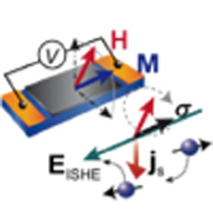 The spin Hall effect is a spin current induced by an electric current, and its occurrence in semiconductors is a promising route to controlling spins and their transport. Here, the inverse spin Hall effect, in which an electric current is induced by a spin current, is observed in silicon for the first time.
Silicon is a group IV semiconductor having the diamond structure. This material has had a crucial role in exploring the physics of semiconductors. Silicon has been broadly viewed as an ideal host also for spintronics owing to its low atomic mass, crystal inversion symmetry, and near lack of nuclear spin, resulting in the exceptionally long spin lifetime1,2,3.
Along with long spin lifetimes, key elements for spintronics are generation and detection of spin currents4,5,6,7,8,9,10,11. A promising method is the utilization of the direct and inverse spin Hall effects (DSHE/ISHE), which convert a charge current into a spin current and vice versa12,13,14,15,16,17,18,19,20,21,22,23,24,25,26,27,28,29,30. However, the underlying origin of the spin Hall effects is the spin–orbit interaction and, thus, it is natural to expect that the spin Hall effects are not accessible in a material that shows long spin lifetimes, such as silicon. Generation of spin currents from an electric field through the spin–orbit interaction, the DSHE, was first observed in gallium arsenide (GaAs) using optical detection techniques, a Kerr-microscopy and a two-dimensional light-emitting diode17,18. Although these optical techniques have had a crucial role for investigating the physics of the DSHE17,18,19,21,28, the application range of the techniques is limited to direct bandgap semiconductors with strong spin–orbit interaction; the indirect bandgap of silicon precludes using these techniques, making it difficult to explore the DSHE in silicon along with its very weak spin–orbit interaction.
The spin–orbit interaction responsible for the DSHE also causes the conversion of a spin current into an electric field, the ISHE25,26,27, which could offer a way to circumvent the above obstacle in exploring the spin Hall effects. The ISHE enables the electric measurement of the spin/charge conversion through the spin–orbit interaction, as demonstrated, for example, in platinum and gallium arsenide22,25,26,29. The electric field EISHE generated by the ISHE from a spin current js with the spin-polarization vector σ is described as25
| 1 |
where  is the spin Hall angle, σSHE and σN are the spin Hall conductivity and electric conductivity, respectively, and ρN is the electric resistivity. Equation (1) shows that the magnitude of the electric field due to the ISHE is proportional to the resistivity ρN of the material, indicating that the ISHE enables sensitive detection of spin currents especially in high-resistivity materials, such as semiconductors.
Although spin injection efficiency into semiconductors is drastically limited by the impedance mismatch problem31, recent advances revealed that efficient spin injection is possible using hot-electron injection32, tunnel barriers33,34, and spin pumping35. In particular, the generation of spin currents from magnetization precession36,37, a recently discovered method utilizing spin pumping, enables high-density spin current injection into a macroscopic area35, which is difficult to achieve by other methods. This is beneficial for enhancing the electric voltage  due to the ISHE; VISHE is proportional both to the spin current density js and length wF of the sample along EISHE. The combination of the spin pumping and ISHE has been observed and is a well-established technique in metallic systems38. This has also been applied to semiconductors with strong spin–orbit interaction, enabling the observation of the ISHE in heavily doped n- and p-type GaAs35. In this work, we experimentally demonstrate that the combination of the ISHE and spin pumping provides a route for exploring the spin/charge current conversion in high-resistivity materials with weak spin–orbit interaction by showing successful measurement of the ISHE in silicon at room temperature.
Results
Detection of inverse spin Hall effect in silicon
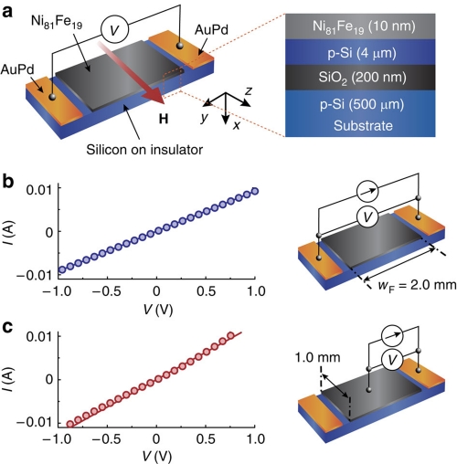
Figure 1a shows a schematic illustration of the sample used in this study. The sample is a Ni81Fe19/B-doped Si (Ni81Fe19/p-Si) film with a doping concentration of NA=2×1019 cm−3 (see Methods). Two ohmic contacts were attached on the p-Si layer (Fig. 1a,b). Here the current-voltage characteristic shown in Figure 1c shows an almost ohmic behaviour at the Ni81Fe19/p-Si interface, suggesting strong dynamical exchange interaction Jex between the magnetization in the Ni81Fe19 layer and carrier spins in the p-Si layer35.
Figure 1. Experimental set-up.
(a) A schematic illustration of the Ni81Fe19/p-Si film used in this study. H represents an external magnetic field. (b) Current-voltage (I–V) characteristic measured for the Ni81Fe19/p-Si film, where the two electrodes are attached to the AuPd layers. wF is the length of the Ni81Fe19 layer. (c) I–V characteristic measured for the Ni81Fe19/p-Si film. The two electrodes are attached to the Ni81Fe19 layer and AuPd layer, respectively.
We measured the ferromagnetic resonance (FMR) signal and electric-potential difference V between the electrodes attached to the p-Si layer to detect the ISHE35; in the FMR condition, the spin pumping driven by the dynamical exchange interaction injects pure spin currents into the p-Si layer. This spin current gives rise to an electric voltage VISHE through the ISHE in the p-Si layer. During the measurements, the Ni81Fe19/p-Si sample was placed at the centre of a TE011 microwave cavity with the frequency of f=9.45 GHz, where the microwave magnetic field was applied along the y direction (Fig. 1a). An external static magnetic field H was applied along the film plane as shown in Figure 1a. All of the measurements were performed at room temperature.
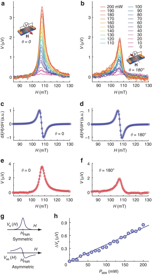
Figure 2a,b shows the DC electromotive force signals measured for the Ni81Fe19/p-Si film at various microwave excitation power, when the external magnetic field H is applied along the film plane at θ=0 and θ=180° (see the insets), respectively. Here θ is the out-of-plane angle of H. In the V spectra, clear electromotive force signals are observed around the ferromagnetic resonance field HFMR (compare the V spectra with the FMR spectra shown in Fig. 2c,d). Figure 2c,d shows that the microwave absorption intensity I is identical for θ=0 and 180°. In contrast, importantly, the magnitude of the electromotive force V is clearly changed by reversing the magnetic field direction as shown in Figure 2a,b; this distinctive behaviour of V is the key feature of the ISHE induced by the spin pumping35.
Figure 2. Observation of ISHE in silicon.
(a) Field (H) dependence of the electromotive force V measured for the Ni81Fe19/p-Si film when θ=0 at different microwave excitation powers. The external magnetic field is applied along the film plane. Here the background voltage due to the microwave irradiation is subtracted from the V spectra. The inset shows a schematic illustration of the experimental set-up when θ=0. (b) H dependence of V measured for the Ni81Fe19/p-Si film when θ=180° at different microwave excitation powers. (c) H dependence of the FMR signal dI(H)/dH measured for the Ni81Fe19/p-Si film when θ=0 at 200 mW microwave excitation (see the inset to a). I is the microwave absorption intensity. The solid circles are the experimental data. The solid curve shows the fitting result using the first derivative of a Lorentz function. (d) H dependence of dI(H)/dH for the Ni81Fe19/p-Si film when θ=180° at 200 mW microwave excitation (see the inset to b). (e) H dependence of V for the Ni81Fe19/p-Si film when θ=0. The solid circles are the experimental data. The solid curve shows the fitting result using  with the parameters Vs=3.50 μV and Vas=−0.41 μV. (f) H dependence of V measured for the Ni81Fe19/p-Si film when θ=180°. The solid curve shows the fitting result with the parameters Vs=1.76 μV and Vas=0.41 μV. (g) The spectral shape of the symmetric Vs (H) and asymmetric Vas (H) components of the electromotive force V (H). (h) Microwave power PMW dependence of ΔVs, where
  . The solid circles are the experimental data. The solid line shows the linear fit to the data.
The electromotive force observed here is the combination of the ISHE in the p-Si layer, the ordinary Hall effect (OHE) in the p-Si layer, the anomalous Hall effect (AHE) in the Ni81Fe19 layer, and heating effects. The direct contribution from the ISHE in the p-Si layer can be extracted as follows (see Methods). The OHE and AHE voltages can be ruled out from the observed electromotive force by fitting the V spectra using a combination of symmetric  (absorption shape) and asymmetric
  (dispersion shape) functions25,
  , where HFMR is the resonance field. Figure 2e,f is the fitting result for the V spectra at 200 mW for θ=0 and θ=180°, respectively, showing that the observed V spectra are well reproduced with Vs=3.50 μV and Vas=−0.41 μV for θ=0 and Vs=1.76 μV and Vas=0.41 μV for θ=180°. What is notable is that the Hall voltage due to rectification changes its sign across HFMR as shown in Figure 2g (ref. 25). In contrast, the electromotive force due to the ISHE is proportional to the microwave absorption intensity38. Here Vs is attributed to both the ISHE in the p-Si layer and heating effects35. To eliminate the heating effects arising from the microwave absorption from the V spectra, we define
  , as the ISHE voltage due to the spin pumping changes its sign by reversing H whereas the electromotive force due to the heating effects is independent on the H direction. In Figure 2h, we show the microwave power PMW dependence of ΔVs. ΔVs increases linearly with PMW, as expected for the ISHE induced by the spin pumping38. ΔVs signal disappears when an in-plane magnetic field is applied parallel to the direction across the electrodes, supporting that ΔVs is attributed to the ISHE in the p-Si layer because of equation (1).
Spin precession and inverse spin Hall effect
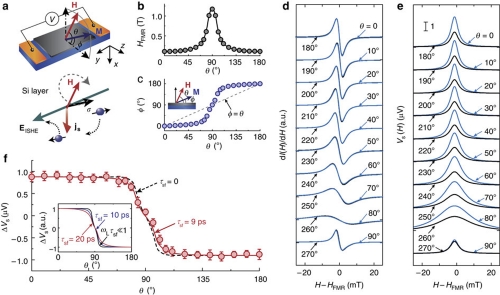
To further buttress the above result, we measured the out-of-plane magnetic field angle θ dependence of ΔVs, which provides further evidence that the observed ΔVs signals are attributed to the ISHE induced by the spin injection in the p-Si layer. Here the out-of-plane magnetic field angle θ is defined in Figure 3a. As shown in Figure 3a, when H is applied oblique to the film plane, the magnetization precession axis is not parallel to H because of the demagnetization field in the Ni81Fe19 layer. The relation between the external magnetic field angle θ and the angle of magnetization–precession axis φ can be obtained using the Landau–Lifshitz–Gilbert equation with the measured values of the resonance field HFMR shown in Figure 3b (ref. 38). The θ dependence of φ for the Ni81Fe19/p-Si film is shown in Figure 3c. In Figure 3d,e, we show the dI/dH and Vs(H) signals for the Ni81Fe19/p-Si film at different θ. As shown in Figure 3e, ΔVs disappears when the external magnetic field is applied perpendicular to the film plane; the θ dependence of ΔVs shows the drastic variation of ΔVs around θ=90° (Fig. 3f). Here the spin-polarization vector σ of the spin current injected into the p-Si layer is parallel to the magnetization–precession axis. Therefore, the spins of the spin current precess around the axis parallel to H, as shown in Figure 3a. This is described in the Bloch equation with spin diffusion and precession in the p-Si layer:
Figure 3. Angular dependence of ISHE signal and spin precession.
(a) A schematic illustration of the Ni81Fe19/p-Si film when the external magnetic field H is applied oblique to the film plane. M denotes the static component of the magnetization. θ and φ show the magnetic field angle and magnetization angle, respectively. (b) Magnetic field angle θ dependence of the FMR field HFMR measured for the Ni81Fe19/p-Si film. The filled circles represent the experimental data. The solid curve is the numerical solution of the Landau–Lifshitz–Gilbert equation with the saturation magnetization 4πMs=0.852T. (c) Magnetic field angle θ dependence of the magnetization angle φ for the Ni81Fe19/p-Si film estimated using the Landau–Lifshitz–Gilbert equation with the measured values of HFMR. (d) Magnetic field angle θ dependence of the FMR signal dI(H)/dH measured for the Ni81Fe19/p-Si film at 200 mW. (e) Magnetic field angle θ dependence of the symmetric component of the electromotive force Vs (H) extracted by a fitting procedure from the measured V spectra for the Ni81Fe19/p-Si film at 200 mW. (f) Magnetic field angle θ dependence of ΔVs. The solid circles are the experimental data. The solid curve is the theoretical curve obtained from equation (5) with τsf=9 ps. The dashed curve is the theoretical curve for τsf=0. The error bars represent the 90% confidence interval. The inset shows the θ dependence of ΔVs calculated from equation (5) with τsf=20 ps (the red curve), τsf=10 ps (the blue curve), and  (the black curve).
 |
2 |
where m(x, t) is the magnetization of carriers in the p-Si layer; γc and τsf are the gyromagnetic ratio and spin relaxation time of carriers in the p-Si layer, respectively; DN is the diffusion constant in the p-Si layer; ex and ez are the unit vector parallel to the x and z axes, respectively (Fig. 3a); δ(x) is the delta function and 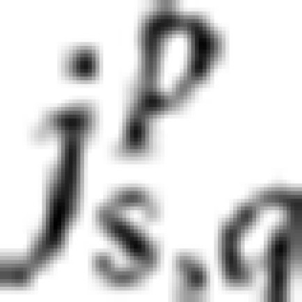 is the spin current density with the spin orientation direction p and flow direction q at the interface x=0. Thus
  and
and  , where the spin current density js generated by the spin pumping at the interface in the FMR condition is given by38,
 |
3 |
Here 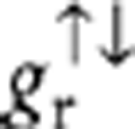 is the spin mixing conductance, γ and Ms are the gyromagnetic ratio and saturation value of the magnetization M, respectively; α is the Gilbert damping constant; h is the microwave magnetic field; and ω=2πf is the angular frequency of the magnetization precession. By solving equation (2) for the equilibrium condition (∂m/∂t=0), we obtain
 |
4 |
where  and
and  ;
;  is the spin diffusion length of the Si layer;
 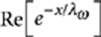 and
and 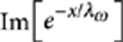 are the real and imaginary part of
 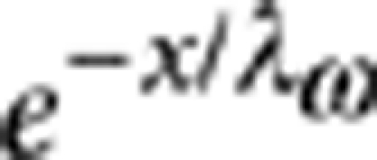 , respectively. Because the spin current flows along the x direction, the electric field induced by the ISHE, EISHE(x), is proportional to
 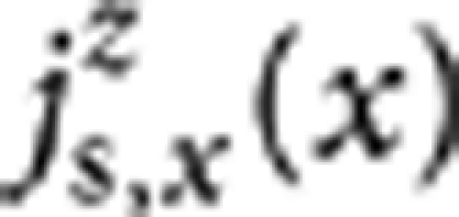 . As shown in Figure 4a,
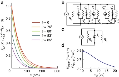
 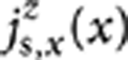 decays because of the spin relaxation in the p-Si layer; the charge current density jc(x) generated by the ISHE also depends on x, which induces short circuit currents in the Ni81Fe19 and p-Si layers38. Equivalent circuit models of the Ni81Fe19/p-Si film are shown in Figure 4b,c (see Methods). Therefore, we obtain the angular dependence of the ISHE signal VISHE in the presence of spin precession as35
Figure 4. Spin current relaxation.
(a) The spin current density 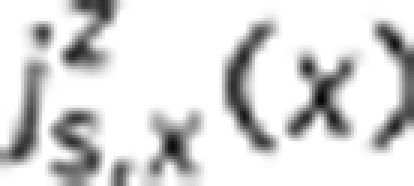 generated by the spin pumping for τsf=9 ps. Here
  is the spin current density at the interface when the external magnetic field is applied along the film plane (θ=0). The parameters used for the calculation are shown in the text. (b) An equivalent circuit model of the Ni81Fe19/p-Si film. RF is the electrical resistance of the Ni81Fe19 layer. (c) A simplified equivalent circuit model of the Ni81Fe19/p-Si film. (d) The spin relaxation time τsf dependence of the ISHE signal VISHE at θ=80° calculated from equation (5).
 |
5 |
where dN is the thickness of the p-Si layer. From equation (5), the electromotive force without taking into account spin precession ( ) is given by
  , which is valid for materials where the spin relaxation time is very fast, such as Pt (ref. 38). Here, calculated θ dependence of ΔVs is shown in the inset of Figure 3f for
  (the black curve), τsf=10 ps (the blue curve), and τsf=20 ps (the red curve) with 4πMs=0.852 T. As τsf increases, spin precession reduces the electromotive force; the drastic variation of ΔVs around θ=80° for
  becomes gentle for τsf=10 ps and τsf=20 ps owing to spin precession. The experimentally measured θ dependence of ΔVs is well reproduced using equation (5) with τsf=9±3 ps as shown in Figure 3f, where ΔVs is obtained from Figure 3e. This is the direct evidence of the observation of the ISHE in the p-Si layer; the ΔVs signal cannot be attributed to the ISHE in the Ni81Fe19 layer, as the spin relaxation time in Ni81Fe19, τsf=9 fs, is so fast that
  is satisfied (see the dashed curve in Fig. 3f), where τsf is obtained from the spin diffusion length39
λF=3 nm and diffusion constant40
DF=10 cm2 s−1. This result also supports that magnetogalvanic effects, that is, the OHE and AHE, and heating effects are irrelevant to ΔVs.
Discussion
The above experimental results allow estimation of the spin Hall conductivity of the p-Si layer. In the FMR condition, when the magnetic field is applied along the film plane, the magnitude of the ISHE signal VISHE is obtained from equation (3) with the equivalent circuit model of the spin-pumping-induced ISHE where short-circuit currents in the Ni81Fe19 layer are taken into account38:  . Here wF, dF and σF are the length defined as in Figure 1b, thickness and electric conductivity of the Ni81Fe19 layer, respectively. Using the parameters for the Ni81Fe19/p-Si film, wF=2.0 mm, DN=3.23 cm2 s−1, dN=4 μm, dF=10 nm, σN=2×10² Ω−1 cm−1, σF=1.5×10⁴ Ω−1 cm−1, 4πMs=0.852T, α=0.0088, h=0.16 mT, τsf=9 ps, and ΔVs=0.87 μV, we find
  m−2. Here the spin mixing conductance
 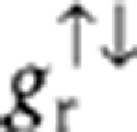 can be obtained from the enhancement of the FMR spectral width due to the spin pumping41. The spin mixing conductance of the Ni81Fe19/p-Si film is estimated from the FMR spectral width for the Ni81Fe19/p-Si film and a Ni81Fe19/SiO2 film as
  m−2. Thus we obtain the spin Hall angle for the p-Si layer θSHE≈1×10⁻⁴, which corresponds to the spin Hall conductivity σSHE≈2×10⁻² Ω−1 cm−1. These values are much smaller than those for doped GaAs28, showing that this approach enables highly sensitive electric measurement of the ISHE. The successful measurement of the ISHE in silicon is attributed to its high electric resistivity, which is essential for large voltage generation due to the ISHE, and the high-density spin injection into macroscopic area by the spin pumping.
Although spin injection into n-type Si has been reported by several groups33,34,42,43, there is only one report of room-temperature spin injection into p-type Si, using tunnel contacts34. The successful observation of the ISHE in the Ni81Fe19/p-Si film now confirms this by a different approach, namely dynamical spin injection. The present experiment shows that the spin relaxation time in the p-Si layer is τsf=9 ps. Here in the direct Ni81Fe19/p-Si contact, the spin relaxation time near the interface may be reduced because of the coupling of the spins in the p-Si layer to the Ni81Fe19 layer44. The spin relaxation time obtained using the electrical spin injection is τsf=270 ps for p-Si with the doping concentration of NA=4.8×1018 cm−3 (ref. 34). Therefore, the spin relaxation time in p-Si obtained by both the electrical and dynamical spin injection is much longer than the momentum relaxation time ~5 fs in the p-Si layer45; understanding the hole spin relaxation in p-type Si remains a challenge.
We showed that silicon has the potential to be used not only as a spin-current-transmission path43,46 but also as a spin-current detector in spite of its weak spin–orbit interaction. Although the spin/charge current conversion efficiency is not large in the p-Si layer, the spin Hall effects in silicon can now be further explored; the combination of the spin pumping and ISHE paves the only way for quantitative exploration of the spin–orbit coupling effect in silicon for different doping density and dopant type. This approach provides also a way to extract the spin relaxation time τsf; as shown in Figure 4d, the magnitude of the electromotive force due to the ISHE is strongly dependent on τsf under the oblique magnetic field, especially when τsf is of the order of 10 ps. Furthermore, the approach presented here, thanks to the high-density spin injection, opens the way for exploring the spin Hall effects in a wide range of materials, including high-resistivity materials with weak spin–orbit interaction. This extends the range of potential materials for spin-current detector without magnetic materials.
Methods
Sample preparation
The sample used in this study is a Ni81Fe19/B-doped Si (Ni81Fe19/p-Si) film with a doping concentration of NA=2×1019 cm−3. Two 30-nm-thick AuPd electrodes were sputtered on a silicon-on-insulator substrate (Fig. 1a) in an Ar atmosphere. After the sputtering, the silicon-on-insulator substrate was annealed at 400 °C for 10 min in a high vacuum, which yields ohmic contacts to the p-Si layer (Fig. 1b). The 10-nm-thick Ni81Fe19 layer was then deposited on the p-Si layer by electron-beam evaporation in a high vacuum. Immediately before the evaporation, the surface of the p-Si layer was cleaned by Ar-ion etching. The surface of the Ni81Fe19 layer and AuPd contact is of a 1.0×2.0-mm2 rectangular shape and of a 1×0.5-mm2 rectangular shape, respectively. The distance from the AuPd contact to the Ni81Fe19 layer is ~300 μm.
Electric voltage due to inverse spin Hall effect
The observed electromotive force in the Ni81Fe19/p-Si film is the combination of the ISHE in the p-Si layer, the OHE in the p-Si layer, the AHE in the Ni81Fe19 layer, and heating effects. The direct contribution from the ISHE in the p-Si layer can be extracted as follows: the OHE in the p-Si layer induces a DC electromotive force from an AC charge current due to a microwave electric field and an AC stray field due to precessing magnetization. This rectified voltage changes its sign across the resonance field, that is, the sign of the electromotive force when H<HFMR is opposite to that when H>HFMR, as the phase of magnetization precession shifts by π at resonance. Therefore, the shape of the electromotive force due to the OHE is asymmetric as shown in Figure 2g. Here a microwave magnetic field cannot create a detectable DC OHE voltage, since the direction of the microwave magnetic field is parallel to the direction across the electrodes (the y direction; Fig. 1a). Furthermore, the microwave magnetic field is independent of the FMR. The shape of the electromotive force due to the AHE is also asymmetric, because it is a rectified voltage induced by the combination of a charge current due to a microwave electric field and precessing magnetization38. In contrast to the rectified voltage due to the OHE and AHE, the electromotive force due to the ISHE is proportional to the intensity of microwave absorption47. This indicates that the shape of the electromotive force due to the ISHE is symmetric as shown in Figure 2g, and, thus, the electromotive force due to the OHE and AHE can be eliminated from the observed electromotive force. The electromotive force due to the sample heating is induced by the Seebeck effect, which is independent on the magnetic field direction. The Seebeck effect in the Ni81Fe19/p-Si film is induced by a lateral temperature gradient along the film plane due to small but finite misalignment of the position of the Ni81Fe19 layer with respect to the substrate. In fact, the magnitude of the symmetric component of V that does not change the sign with reversal of H depends strongly on samples. A longitudinal temperature gradient, that is, a temperature gradient perpendicular to the film plane, may induce a voltage through the Nernst effect. Although the Nernst effect induces a H-dependent voltage, Figure 3f clearly shows that this effect is irrelevant to the ΔVs signals; the variation of ΔVs cannot be reproduced by the cross product of a longitudinal temperature gradient and the external magnetic field. The θ dependence of ΔVs is well reproduced using equation (5) with the spin relaxation time τsf=9 ps for PMW=100, 150 and 200 mW. All errors and error bars represent the 90% confidence interval.
Equivalent circuit model
As shown in Figure 4a, 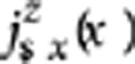 decays because of the spin relaxation in the p-Si layer; the charge current density jc(x) generated by the ISHE also depends on x, which induces short circuit currents in the Ni81Fe19 and p-Si layers38. Here a total charge current generated by the ISHE is
  , where dN is the thickness of the p-Si layer. By dividing the p-Si layer into n layers, an equivalent circuit of the Ni81Fe19/p-Si film is obtained as shown in Figure 4b, where RF is the electrical resistance of the Ni81Fe19 layer. The electrical resistance
  and the charge current
  generated by the ISHE of the ith layer satisfy
  and
and  , where RN is the electrical resistance of the p-Si layer. It is straightforward to convert the circuit shown in Figure 4b into that shown in Figure 4c. Thus, the electromotive force due to the ISHE is obtained as
  . This result shows that VISHE is proportional to the total charge current IN generated by the ISHE; the electromotive force due to the ISHE in the Ni81Fe19 layer is negligibly small because of the extremely short spin diffusion length39 and small spin Hall angle48.
Author contributions
K.A. designed the experiment, collected all the data, performed analysis of the data, and wrote the manuscript. E.S. supervised the study. Both the authors discussed the results and commented on the manuscript.
Additional information
How to cite this article: Ando, K. & Saitoh, E. et al. Observation of the inverse spin Hall effect in silicon. Nat. Commun. 3:629 doi: 10.1038/ncomms1640 (2012).
Acknowledgments
We thank S. Takahashi and R. Takahashi for valuable discussions. This work was supported by the Cabinet Office, Government of Japan through its 'Funding Program for Next Generation World-Leading Researchers,' the Asahi Glass Foundation, the Casio Foundation, the Kurata Foundation, and JST-CREST 'Creation of Nanosystems with Novel Functions through Process Integration'.
References
- Žutić I., Fabian J. & Das Sarma S. Spintronics: fundamentals and applications. Rev. Mod. Phys. 76, 323–410 (2004). [Google Scholar]
- Fabian J., Matos-Abiague A., Ertler C., Stano P. & Žutić I. Semiconductor spintronics. Acta Phys. Slov. 57, 565–907 (2007). [Google Scholar]
- Cheng J. L., Wu M. W. & Fabian J. Theory of the spin relaxation of conduction electrons in silicon. Phys. Rev. Lett. 104, 016601 (2010). [DOI] [PubMed] [Google Scholar]
- Wolf S. A. et al. Spintronics: a spin-based electronics vision for the future. Science 294, 1488–1495 (2001). [DOI] [PubMed] [Google Scholar]
- Johnson M. & Silsbee R. H. Interfacial charge-spin coupling: injection and detection of spin magnetization in metals. Phys. Rev. Lett. 55, 1790–1793 (1985). [DOI] [PubMed] [Google Scholar]
- Jedema F. J., Filip A. T. & van Wees B. J. Electrical spin injection and accumulation at room temperature in an all-metal mesoscopic spin valve. Nature 410, 345–348 (2001). [DOI] [PubMed] [Google Scholar]
- Lou X. et al. Electrical detection of spin transport in lateral ferromagnet-semiconductor devices. Nature Phys. 3, 197–202 (2007). [Google Scholar]
- Crooker S. A. et al. Imaging spin transport in lateral ferromagnet/semiconductor structures. Science 309, 2191–2195 (2005). [DOI] [PubMed] [Google Scholar]
- Lou X. et al. Electrical detection of spin accumulation at a ferromagnet-semiconductor interface. Phys. Rev. Lett. 96, 176603 (2006). [DOI] [PubMed] [Google Scholar]
- Tran M. et al. Enhancement of the spin accumulation at the interface between a spin-polarized tunnel junction and a semiconductor. Phys. Rev. Lett. 102, 036601 (2009). [DOI] [PubMed] [Google Scholar]
- Zhu H. J. et al. Room-temperature spin injection from Fe into GaAs. Phys. Rev. Lett. 87, 016601 (2001). [DOI] [PubMed] [Google Scholar]
- Bakun A. A., Zakharchenya B. P., Rogachev A. A., Tkachuk M. N. & Fleisher V. G. Observation of a surface photocurrent caused by optical orientation of electrons in a semiconductor. JETP Lett. 40, 1293–1295 (1984). [Google Scholar]
- Dyakonov M. I. & Perel V. I. Current-induced spin orientation of electrons in semiconductors. Phys. Lett. 35A, 459–460 (1971). [Google Scholar]
- Hirsch J. E. Spin Hall effect. Phys. Rev. Lett. 83, 1834–1837 (1999). [Google Scholar]
- Murakami S., Nagaosa N. & Zhang S. C. Dissipationless quantum spin current at room temperature. Science 301, 1348–1351 (2003). [DOI] [PubMed] [Google Scholar]
- Sinova J. et al. Universal intrinsic spin Hall effect. Phys. Rev. Lett. 92, 126603 (2004). [DOI] [PubMed] [Google Scholar]
- Kato Y. K., Myers R. C., Gossard A. C. & Awschalom D. D. Observation of the spin Hall effect in semiconductors. Science 306, 1910–1913 (2004). [DOI] [PubMed] [Google Scholar]
- Wunderlich J., Kaestner B., Sinova J. & Jungwirth T. Experimental observation of the spin-Hall effect in a two-dimensional spin-orbit coupled semiconductor system. Phys. Rev. Lett. 94, 047204 (2005). [DOI] [PubMed] [Google Scholar]
- Sih V. et al. Spatial imaging of the spin Hall effect and current-induced polarization in two-dimensional electron gases. Nature Phys. 1, 31–35 (2005). [Google Scholar]
- Stern N. P. et al. Current-induced polarization and the spin Hall effect at room temperature. Phys. Rev. Lett. 97, 126603 (2006). [DOI] [PubMed] [Google Scholar]
- Stern N. P., Steuermann D. W., Mack S., Gossard A. C. & Awschalom D. D. Time-resolved dynamics of the spin Hall effect. Nature Phys. 4, 843–846 (2008). [Google Scholar]
- Wunderlich J. et al. Spin Hall effect transistor. Science 330, 1801–1804 (2010). [DOI] [PubMed] [Google Scholar]
- Tse W.- K. & Das Sarma S. Spin Hall effect in doped semiconductor structures. Phys. Rev. Lett. 96, 056601 (2006). [DOI] [PubMed] [Google Scholar]
- Engel H.- A., Halperin B. I. & Rashba E. I. Theory of spin Hall conductivity in n-doped GaAs. Phys. Rev. Lett. 95, 166605 (2005). [DOI] [PubMed] [Google Scholar]
- Saitoh E., Ueda M., Miyajima H. & Tatara G. Conversion of spin current into charge current at room temperature: inverse spin-Hall effect. Appl. Phys. Lett. 88, 182509 (2006). [Google Scholar]
- Kimura T., Otani Y., Sato T., Takahashi S. & Maekawa S. Room-temperature reversible spin Hall effect. Phys. Rev. Lett. 98, 156601 (2007). [DOI] [PubMed] [Google Scholar]
- Valenzuela S. O. & Tinkham M. Direct electronic measurement of the spin Hall effect. Nature 442, 176–179 (2006). [DOI] [PubMed] [Google Scholar]
- Matsuzaka S., Ohno Y. & Ohno H. Electron density dependence of the spin Hall effect in GaAs probed by scanning Kerr rotation microscopy. Phys. Rev. B 80, 241305(R) (2009). [Google Scholar]
- Garlid E. S., Hu Q. O., Chan M. K., Palmstrøm C. J. & Crowell P. A. Electrical measurement of the direct spin Hall effect in Fe/InxGa1−xAs Heterostructures. Phys. Rev. Lett. 105, 156602 (2010). [DOI] [PubMed] [Google Scholar]
- Brüne C. et al. Evidence for the ballistic intrinsic spin Hall effect in HgTe nanostructures. Nature Phys. 6, 448–454 (2010). [Google Scholar]
- Schmidt G., Ferrand D., Molenkamp L. W., Filip A. T. & van Wees B. J. Fundamental obstacle for electrical spin injection from a ferromagnetic metal into a diffusive semiconductor. Phys. Rev. B 62, R4790–R4793 (2000). [Google Scholar]
- Appelbaum I., Huang B. & Monsma D. J. Electronic measurement and control of spin transport in silicon. Nature 447, 295–298 (2007). [DOI] [PubMed] [Google Scholar]
- Jonker B. T., Kioseoglou G., Hanbicki A. T., Li C. H. & Thompson P. E. Electrical spin-injection into silicon from a ferromagnetic metal/tunnel barrier contact. Nature Phys. 3, 542–546 (2007). [Google Scholar]
- Dash S. P., Sharma S., Patel R. S., de Jong M. P. & Jansen R. Electrical creation of spin polarization in silicon at room temperature. Nature 462, 491–494 (2009). [DOI] [PubMed] [Google Scholar]
- Ando K. et al. Electrically tunable spin injector free from the impedance mismatch problem. Nature Mater. 10, 655–569 (2011). [DOI] [PubMed] [Google Scholar]
- Tserkovnyak Y., Brataas A. & Bauer G. E. W. Enhanced Gilbert damping in thin ferromagnetic films. Phys. Rev. Lett. 88, 117601 (2002). [DOI] [PubMed] [Google Scholar]
- Brataas A., Tserkovnyak Y., Bauer G. E. W. & Halperin B. I. Spin battery operated by ferromagnetic resonance. Phys. Rev. B 66, 060404(R) (2002). [Google Scholar]
- Ando K. et al. Inverse spin-Hall effect induced by spin pumping in metallic system. J. Appl. Phys. 109, 103913 (2011). [Google Scholar]
- Bass J. & Pratt Jr W. P. Spin-diffusion lengths in metals and alloys, and spin-flipping at metal/metal interfaces: an experimentalist’s critical review. J. Phys. Condens. Matter 19, 183201 (2007). [Google Scholar]
- Garcia-Cervera C. J. & Wang X.- P. Advances in numerical micromagnetics: spin-polarized transport. Bol. Soc. Esp. Mat. Apl. 34, 217–221 (2006). [Google Scholar]
- Tserkovnyak Y., Brataas A., Bauer G. E. W. & Halperin B. I. Nonlocal magnetization dynamics in ferromagnetic heterostructures. Rev. Mod. Phys. 77, 1375 (2005). [Google Scholar]
- Ando Y. et al. Electrical injection and detection of spin-polarized electrons in silicon through an Fe3Si/Si Schottky tunnel barrier. Appl. Phys. Lett. 94, 182105 (2009). [Google Scholar]
- Suzuki T. et al. Room-temperature electron spin transport in a highly doped Si channel. Appl. Phys. Exp. 4, 023003 (2011). [Google Scholar]
- Dash S. P. et al. Spin precession and inverted Hanle effect in a semiconductor near a finite-roughness ferromagnetic interface. Phys. Rev. B 84, 054410 (2011). [Google Scholar]
- Ray S. K. et al. Characteristics of THz waves and carrier scattering in boron-doped epitaxial Si and Si1−xGex films. J. Appl. Phys. 95, 5301–5304 (2004). [Google Scholar]
- Dery H., Song Y., Li P. & Žutić I. Silicon spin communication. Appl. Phys. Lett. 99, 082502 (2011). [Google Scholar]
- Ando K. et al. Electric detection of spin wave resonance using inverse spin-Hall effect. Appl. Phys. Lett. 94, 262505 (2009). [Google Scholar]
- Tanaka T., Kobayashi I., Takahashi M. & Wakiyama T. Anisotropic magnetoresistance and Hall effects for Ni-Fe-M alloy thin films. IEEE Trans. Magn. 26, 2418 (1990). [Google Scholar]


