Abstract
This paper investigates the performance of 1 mm resolution Cadmium Zinc Telluride (CZT) detectors for positron emission tomography (PET) capable of positioning the 3-D coordinates of individual 511 keV photon interactions. The detectors comprise 40 mm × 40 mm × 5 mm monolithic CZT crystals that employ a novel cross-strip readout with interspersed steering electrodes to obtain high spatial and energy resolution. The study found a single anode FWHM energy resolution of 3.06±0.39% at 511 keV throughout most the detector volume. Improved resolution is expected with properly shielded front-end electronics. Measurements made using a collimated beam established the efficacy of the steering electrodes in facilitating enhanced charge collection across anodes, as well as a spatial resolution of 0.44±0.07 mm in the direction orthogonal to the electrode planes. Finally, measurements based on coincidence electronic collimation yielded a point spread function with 0.78±0.10 mm FWHM, demonstrating 1 mm spatial resolution capability transverse to the anodes – as expected from the 1 mm anode pitch. These findings indicate that the CZT-based detector concept has excellent performance and shows great promise for a high-resolution PET system.
Keywords: CZT, semiconductor detector, cross-strip electrode, charge collection, high resolution, PET, small animal
1. Introduction
We are developing an ultra-high-resolution PET detector system built out of Cadmium Zinc Telluride (CZT) detectors. This paper investigates the energy and spatial resolution performances of a 1 mm resolution 40 mm × 40 mm × 5 mm monolithic CZT crystal detector capable of positioning the 3-D coordinates of individual 511 keV photon interactions. The detector is intended for a 3-D high-resolution small animal PET system, and it is patterned with a novel cross-strip electrode design that includes steering electrodes to enhance charge collection.
Measurements resulting from this study provide the basis for determining the design specifications and optimizations for the small animal PET system’s data acquisition, signal processing, and image reconstruction components.
Topics presented in subsequent sections include the CZT detector design, the experimental setups used, results and analyses pertaining to the detector’s single anode and multiple anode energy spectra and resolution, efficacy of charge steering electrodes, spatial resolution in the direction orthogonal to the electrode planes (DOEP), as well as anode spatial resolution. The paper ends with a discussion of future work and conclusions.
2. Cadmium zinc telluride crystal as an annihilation photon detector
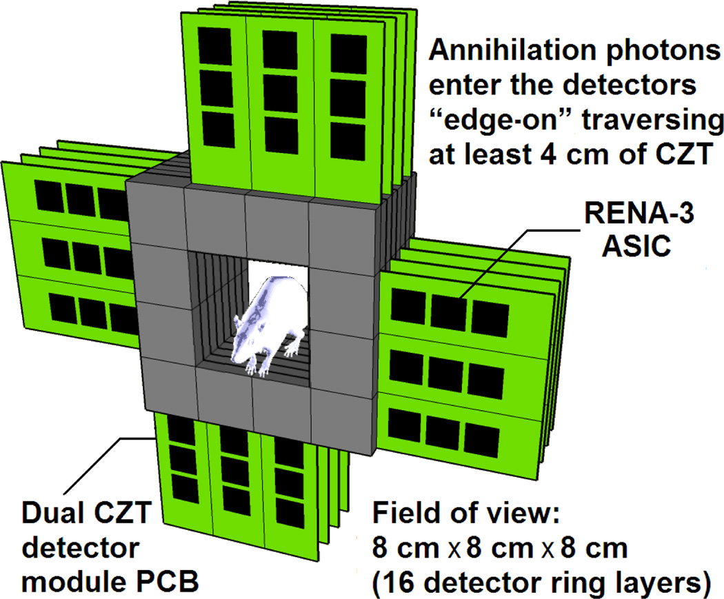
A number of research efforts and designs have been made aiming to achieve ~1 mm resolution in small animal PET (Missimer et al 2004, Yang et al 2004, Vaska et al 2005a, Sempere Roldan 2007, Spanoudaki et al 2007, Bergeron et al 2009), which is an especially appropriate application of CZT given its properties as a 511 keV photon detector material (Vaska et al 2005b, Zhang et al 2005, Mitchell et al 2008, Morimoto et al 2010). Figure 1 shows the high resolution 8 cm × 8 cm × 8 cm field of view (FOV) CZT small animal PET system for which the detector studied is intended (Levin et al 2004a, Habte et al 2007, Matteson et al 2008, Pratx and Levin 2009). In this “edge-on” detector arrangement, the CZT detectors offer greater than 99% inter-module packing fraction, and the 4 cm thickness of CZT promotes greater than 86% intrinsic detection efficiency for single 511 keV photons (>73% for coincident pairs) (Levin et al 2006, Habte et al 2007). A second advantage of CZT detectors is that their intrinsic spatial resolution is defined by the electrode pattern, and not limited by the ability to manufacture and handle arrays of miniscule crystal elements as is required to achieve high resolution with scintillation crystal-based detectors (Levin et al 2004a, Levin 2008, Matteson et al 2008).
Figure 1.
CZT high-resolution small animal PET system under development.
Thirdly, the anode and cathode signal amplitudes and/or charge drift time allow one to estimate the individual (multiple) 3-D interaction coordinates of incoming photons in a CZT detector (Kalemci et al 1999, Li et al 2000, Hong et al 2003). This allows for accurate placement of lines of response required for PET imaging (Pratx and Levin 2009). Lastly, CZT detectors can offer excellent energy resolution (better than 3% FWHM) at 511 keV (Levin et al 2006, Levin 2008) to help mitigate tissue scatter, random and multiple coincidence background as well as enabling more accurate event positioning (Pratx and Levin 2009).
There are however also a number of challenges in working with CZT. One concern is the electrode contact robustness. The detector’s semiconductor-metal junction is formed between CZT and metal electrodes deposited on the detector surface. The gold electrodes we use are extremely thin (much less than 1 µm), they can therefore be easily scratched or damaged through handling and repeated coupling to readout electronics.
A second challenge is the lower atomic number of CZT compared to scintillation materials commonly used in PET systems such as lutetium oxyorthosilicate (LSO). The corresponding relatively low photo-fraction in CZT means Compton scattering interactions dominate. In fact, simulations based on the small animal imaging system predicts that a 511 keV incoming photon would on average undergo ~2.3 interactions before being absorbed in the system’s CZT detector volume (Pratx and Levin 2009). Consequently the system should aim to have the ability to acquire and process multiple interaction photon events in order to maintain high photon sensitivity. Such systemic demand is not unique to CZT however, but present for high-resolution PET systems that use miniscule (e.g. <2 mm) LSO scintillation crystals as well. For example, both experimental and simulation results have shown that the probability of incoming annihilation photon to scatter from one 1 mm LSO crystal element into another can be as high as ~71% (Levin et al 2004b, Gu et al 2010). In this case, as with CZT, the LSO-based system would also need to have the capability to acquire and analyze multiple interaction photon events.
With Compton scattering dominating, a large number of interactions will have energy deposition much less than 511 keV corresponding to small amplitude signals. Since there is no internal signal amplification mechanism in CZT as there is in scintillation detectors, specially-designed low-noise, charge-sensitive readout electronics are required.
Thirdly, in CZT the fundamental mechanism of signal generation is the induction of charge on electrodes due to the drift of charge carriers (electrons and holes). Since the electrode sensitivity to charge carriers is spatially varying, CZT detectors produce signals with relatively high temporal variance compared to the propagation and collection of scintillation light. This means CZT detectors have more timing jitter and time walk, which degrades the coincidence time resolution.
A final challenge in building a CZT-based PET system is that if good spatial resolution is desired, the system requires a large number of cathodes and anodes, and, since analogue multiplexing is typically not possible due to the relatively small signals, a large number of signal readout channels are needed. This can be a challenge in terms of data acquisition bandwidth, interconnect density and thermal management.
3. The CZT detector design
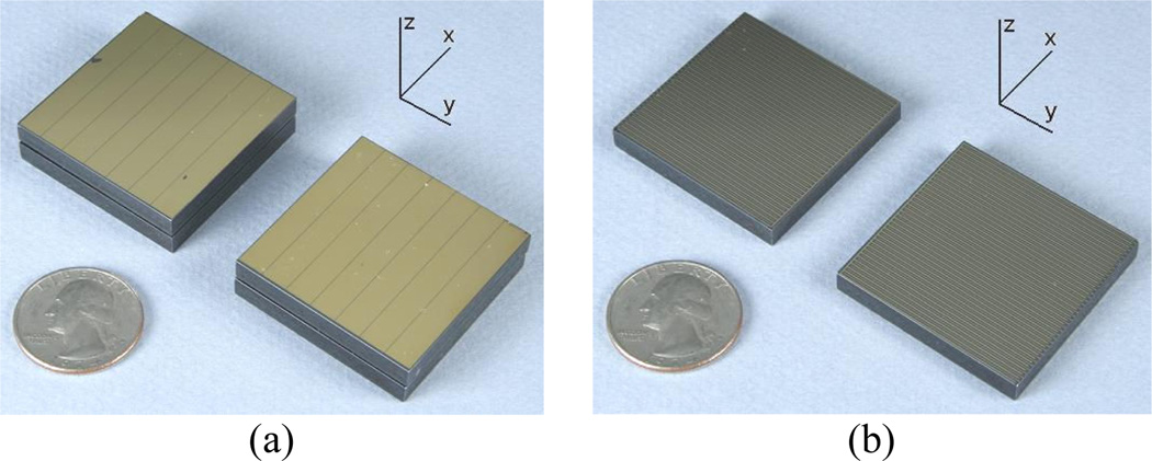
Figure 2 shows the CZT detector design. Each detector is a monolithic CZT crystal slab of dimension 40 mm × 40 mm × 5 mm. Orthogonal gold anode and cathode strips that span the entire width of the crystal are deposited on opposite 40 mm × 40 mm faces of the crystal slab. The cross-strip electrode pattern was chosen to provide high spatial resolution for x–y localization of photon interactions while using fewer electronic channels compared to standard square pixel designs e.g. Mashlum et al (2007), that is, 2n versus n2.
Figure 2.
Cathode side (a) and anode side (b) of the 40 mm × 40 mm × 5 mm cross-strip CZT detector. The cathode strips in this prototype electrode pattern are 5.4 mm wide on a 5.5 mm pitch, the anode strips are 0.1 mm wide on a 1 mm pitch.
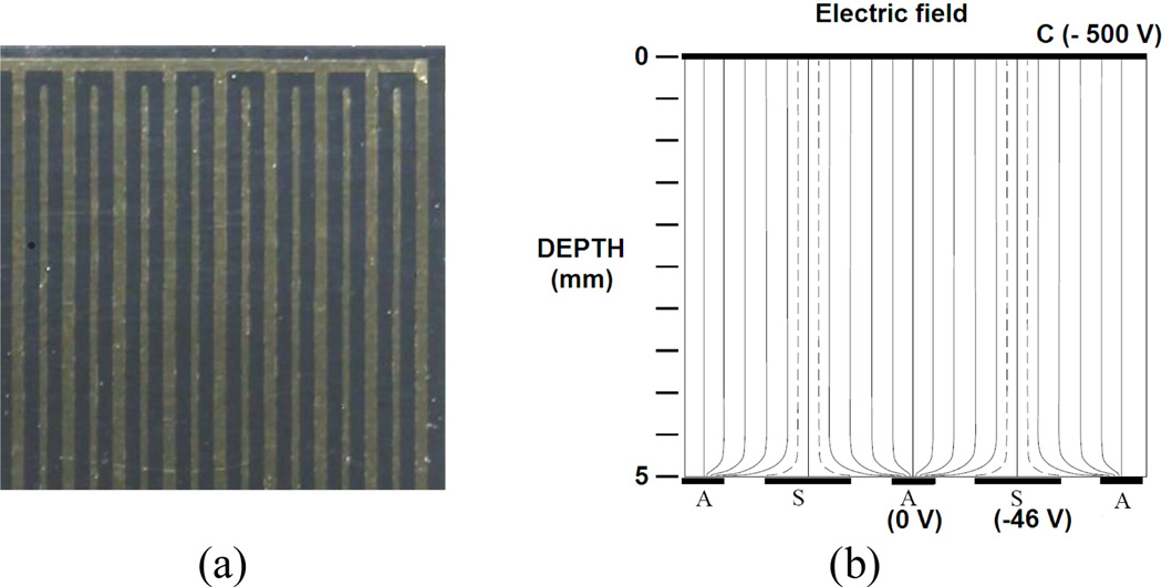
In the prototype, seven cathodes span the one face of the CZT crystal (figure 2(a)). The cathodes have a width of 5.4 mm and a pitch of 5.5 mm. Thirty eight anodes span the opposite face of the crystal (figure 2(b)), they have a width of 0.1 mm and are on a 1.0 mm pitch. The small width of the anodes produces a strong so-called “small-pixel effect” (Barrett et al 1995, Luke 1996, see also section 5.1) which mitigates anode signal deficit due to slow-moving holes. The anodes are interspersed with steering electrodes with the same pitch (figure 3(a)) and of width 0.2 mm in order to enhance anode charge collection.
Figure 3.
Figure 3(a) shows interspersed anodes (thin) and steering electrodes (thick), and figure 3(b) shows the effect of steering electrodes on electric field lines (adapted from Matteson et al 2002).
The operation of CZT photon detectors requires the application of a high-voltage bias across the detector crystal. Under applied bias, an electric field is established that causes mobile charge carriers to drift towards either the anodes (electrons) or the cathodes (holes). If we further set the steering electrodes at a slightly lower potential relative to the anodes, the electric field lines then no longer terminate normal to the anode plane. Instead, they bend towards and concentrate around the anodes. The result is that when photon interactions occur within the volume subtended by the gaps between anode strips, the bent field lines steer the drifting charge carriers away from the gaps toward the anode strips (figure 3(b)). The steering electrodes therefore effectively funnel charge carriers towards anodes for more complete charge collection on anodes (Kalemci et al 1999, Matteson et al 2002).
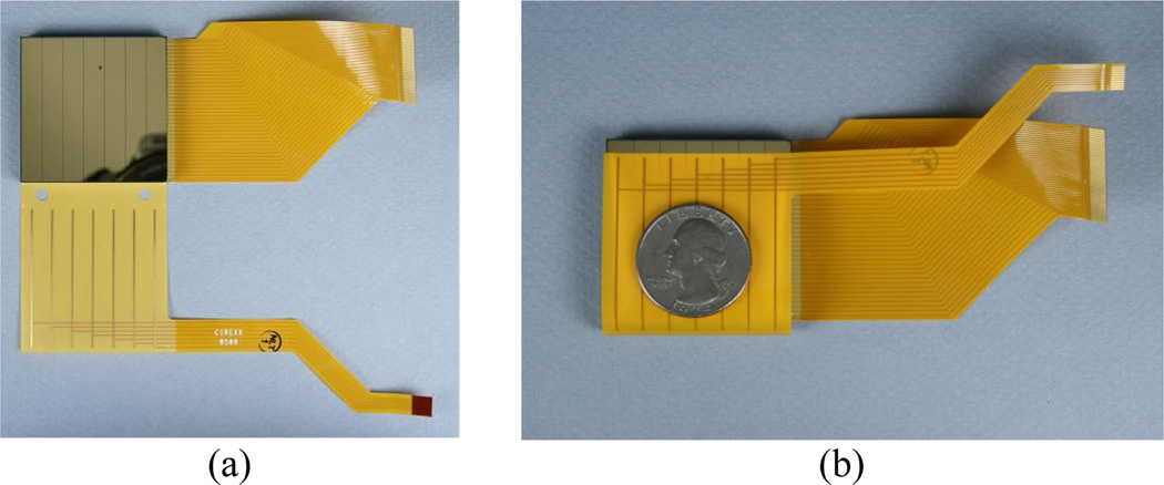
Figure 4(a) shows the flex circuit designed to provide electrical connection between the CZT detectors and the data acquisition system. The flex circuit was formed by etching the traces out of a copper-coated Kapton layer followed by gold plating of the traces. The flex circuit is wrapped around a detector as shown in figure 4(b) so that its gold contacts couple to the electrodes. The contacts facilitate routing of electronic signals to preamplifier inputs via printed circuit board connectors.
Figure 4.
Pictures of CZT detector and flex circuits patterned with traces that match the pitch of the cross-strip electrode pattern. Figure 4(a) shows a CZT detector resting on flex circuits with the cathode side up, and figure 4(b) shows flex circuits coupled to detector electrodes.
4. Experimental setup and methods
4. 1. General detector and electronic readout connections
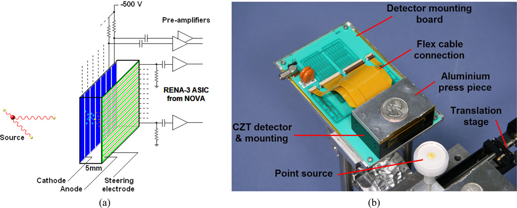
A bias of −500 V was applied to the cathodes with respect to the anodes, which are held at virtual ground potential. The detector anode and cathode outputs are connected to pull-up and pull-down resistors respectively and AC coupled to the preamplifier inputs (figure 5(a)). The steering electrodes were held at −46 V with respect to the anodes.
Figure 5.
CZT photon detector electrical and mechanical connections. Figure 5(a) shows a detector’s high-voltage bias and electronic connections, and figure 5(b) shows the detector mounting assembly.
The front-end signal readout system comprised primarily of RENA-3 (Readout Electronics for Nuclear Applications developed by NOVA R&D Inc., Riverside, CA) application specific integrated circuits (ASIC). The RENA-3 ASIC was designed specifically to perform pre-amplification and shaping of semiconductor photon detector pulses, as well as to provide a trigger, sample-and-hold, and fast time stamps for each detected photon interaction to facilitate coincidence detection (settings at gain = 3, shaping time = 2.8 µs and average trigger threshold = 60 keV). The ASIC’s time pick-off is based on a leading-edge discriminator, and a fast ADC digitises the sampled peak pulse amplitude for each event. Average data acquisition trigger thresholds were 63 keV and 57 keV for the anodes and cathodes, respectively.
The CZT detector is placed inside a detector housing and secured in place by a 4 mm thick aluminium press piece (figure 5(b)). The detector housing is in turn mounted on a printed circuit board, which hosts the high-voltage bias resistors, AC coupling capacitors as well as connectors for the flex circuits and connection to RENA-3 ASICs.
4.2. Anode energy resolution experiments
The single and multiple interaction event energy resolution studies were performed based on the edge-on irradiation configuration as described here. As shown in figure 5(b), a 10 µCi, 250 µm diameter 22Na point source was placed 20 mm in front of the centre of the detector’s 40 mm × 5 mm edge-face so that the photons entered the crystal edge-on (as would be the case when the detectors are assembled in the small animal PET system of figure 1, where the photons would encounter at least 4 cm of CZT material). The detector was oriented such that the anode strips were pointed toward the source.
The “multiple interaction” event energy resolution mentioned above refers to that of an energy spectrum containing events that deposit energy across multiple distinct anodes. The total energy of these events is recovered by summing signals from the anodes that simultaneously triggered. These “multiple-anode” events include charge-shared events, which arise when photon interactions occur along the charge detection volume boundary between anode strips, as well as events involving Compton scatter, which is prevalent in CZT as noted in section 1. The energy resolution pertaining to multiple-anode events is of particular interest since the ability to acquire and reconstruct multiple interaction photon events would allow the system to have higher photon sensitivity than if only events within the 511 keV photopeak of 22Na were acquired.
Calibration of signal amplitude to energy in keV was performed for each anode channel to account for gain and offset variations across anode channels; this is so that signals from across different anodes can be meaningfully added in multiple interaction events. A linear mapping was obtained by taking note of the ADC channel values corresponding to photopeaks at known energies (22Na and 137Cs), from which the ADC channel value corresponding to 0 keV and the keV/ADC channel conversion factor were then calculated.
Where appropriate, the FWHM energy resolution at 511 keV was calculated after correction for depth-dependent signal deficit in the anode energy spectra, the depth is defined as being along the z direction in figure 2. Depth-dependent effects are discussed in detail in section 6.1, but briefly, interactions near the anode plane create trapped and slowly-moving holes near the anodes (collectively referred to as hole trapping), which induces a signal component with opposite polarity to that of electrons attracted by the anode. This results in smaller anode signals, and in the case of photoelectric events this results in an anode spectral photopeak broadened towards lower energies, also known as “low energy tailing”. The severity of this signal deficit has a systematic dependence on photon interaction depth along the z axis. The study results will show that the cathode-to-anode ratio (C/A ratio), defined as the digitised cathode signal amplitude divided by the anode signal amplitude, allows one to accurately estimate the photon interaction depth. This in turn enables the abovementioned photopeak broadening toward lower energies to be corrected by calibrating the anode signal deficit as a function of the C/A ratio via the semi-empirical formula:
| (1) |
The coefficients ai were fitted to anode vs. C/A data so that the function evaluates the expected measured anode energy for 511 keV photoelectric events at any given interaction depth. The depth dependence is then accounted for by multiplying anode energy measurements with the appropriate correction factor (CF), i.e. CF(C/A) = 511keV/Ephotopeak(C/A).
Energy resolution at the 511 keV photopeak was calculated by fitting the following function:
| (2) |
E and an denote the energy of interaction and fitted parameters, respectively. The first two terms of the expression account for the background counts and the last term is a Gaussian curve modelling the photopeak. The FWHM energy resolution is derived as Energy ResolutionFWHM = 2.35a5.
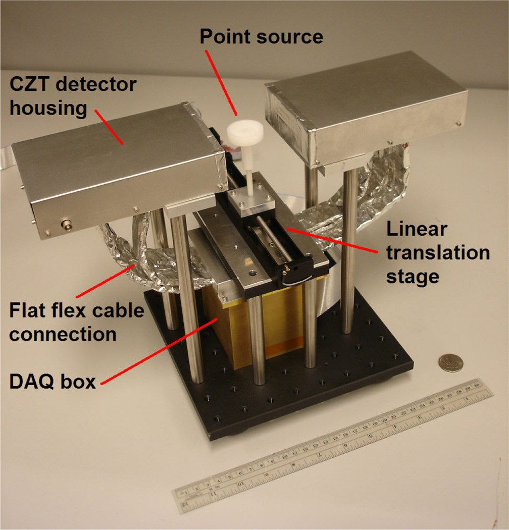
To probe whether the detector’s anode energy resolution had any dependence on the position (transverse to the anodes) of photon interactions within a single anode pitch, the coincidence collimation setup of figure 6 was used. The second detector used for coincidence detection (electronic collimation) was an identical CZT detector assembly positioned so that the 40 mm × 5 mm edge-faces of the two detectors were opposite-facing, parallel and positioned 40 mm apart. The 22Na point source was placed on the centre line between the pair of detectors atop a precision linear translation table, which moved the source along the centre line at 167 µm increments across anode pitches.
Figure 6.
Coincidence detector setup comprising two “edge-on” CZT detector pairs.
Electronic collimation ensured the collimated photons entered the detector perpendicularly with respect to its 40 mm × 5 mm edge-face. This was achieved by seeking coincident signals from anode strips in the two detectors that are located directly opposite each other across the 40 mm separation between the detectors. In particular, only coincident events that triggered exactly one anode and one cathode strip in each detector were considered.
For the geometry and source activity of figure 6, the average time interval between consecutive photon interactions in each detector is in the order of hundreds of microseconds, hence the random coincidence rate was sufficiently low to allow the RENA-3 acquisition system’s window of 7.2 µs to be used as the coincidence time window before the system’s time resolution is optimised.
4.3. Efficacy of steering electrodes
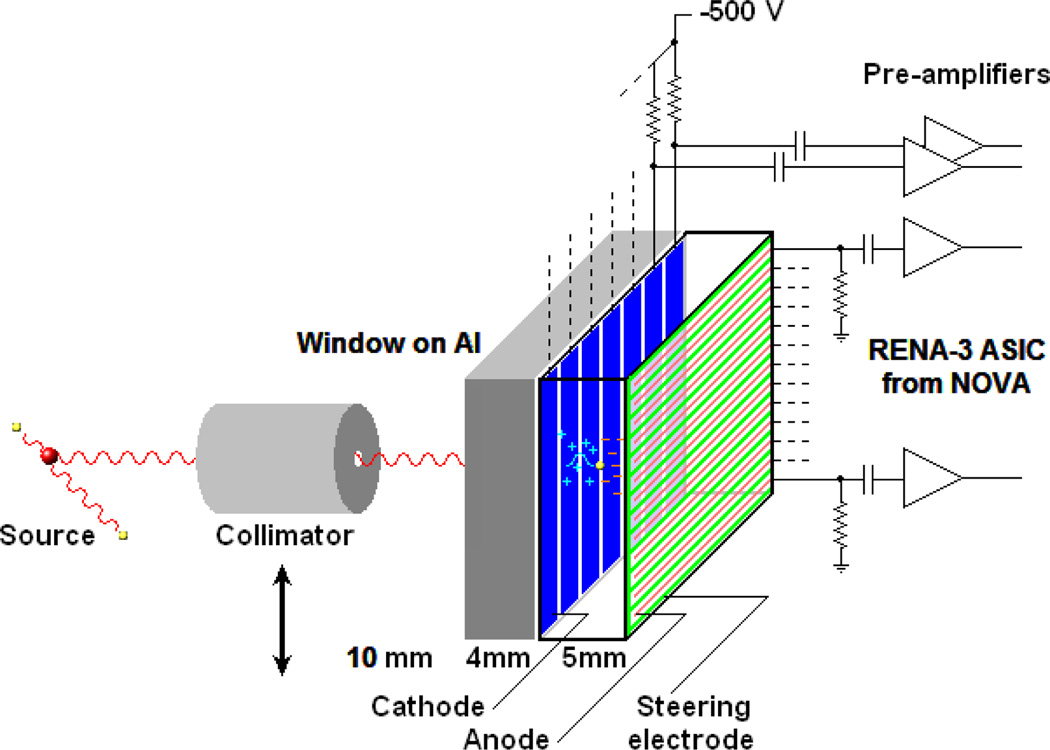
A physically collimated 137Cs gamma ray beam was used for studies characterizing the efficacy of steering electrodes (figure 7). The collimator comprises a tungsten rod of length 14.68 cm and diameter 2.54 cm, surrounded by additional lead shielding. The size of the aperture gradually decreased along the length of the collimator from a 3 mm diameter at the source end to 0.2 mm at the detector end. The collimator was mounted on a position control stage with x–y position control precision of 1 µm.
Figure 7.
Experimental setup characterising the efficacy of steering electrodes. The collimated beam is stepped in the direction indicated by arrow.
The collimated beam was oriented such that it entered the detector orthogonal to the electrode planes (figure 7). To reduce photon scatter due to the beam traversing the thickness of the aluminium press piece, a 1 cm × 1 cm window was cut from the aluminium so that the collimated beam entered the detector unaffected by the metal. The beam was translated, in turn, at a discrete set of positions each 166.6 µm apart across several anode pitches. The range of steering electrode voltages used was −12.85 V, −25.53 V, −49 V, −98 V and −136 V.
4.4. Spatial resolution along the direction orthogonal to the electrode planes (DOEP)
For measuring the detector spatial resolution along the direction orthogonal to the electrode planes (DOEP) i.e. along the z axis as defined in figure 2, a steering electrode bias of −46 V was used. The beam was directed as shown in figure 8 and translated, in turn, at a discrete set of positions each 0.5 mm or 1 mm apart across the thickness of the detector. To determine interaction location in the DOEP, C/A ratio was calculated for all events acquired in each collimated beam position.
Figure 8.
Experimental setup for measuring resolution in the DOEP by stepping the collimated beam in the direction indicated by arrow.
4.5. Anode spatial resolution experiment
The electronic collimation setup described in the last part of section 4.2 was used for the anode spatial resolution study. Instead of studying energy resolution however this part of the study focused on the number of detected coincidences over a fixed time interval as a function of the point source position.
5 Results
5.1. Anode energy resolution
This section presents i) energy spectra of both single and multiple-anode events, ii) energy resolution as a function of DOEP position, and iii) energy resolution as a function of interaction position transverse to the anode pitches.
For a single anode near the centre of the detector illuminated edge-on with an uncollimated point source, the energy spectrum of figure 9 was obtained. The FWHM energy resolution of the 511 keV photopeak before correction for depth-dependent signal deficit is 4.09±0.14%. Note that broadening or tailing is visible on the low energy side of the photopeak.
Figure 9.
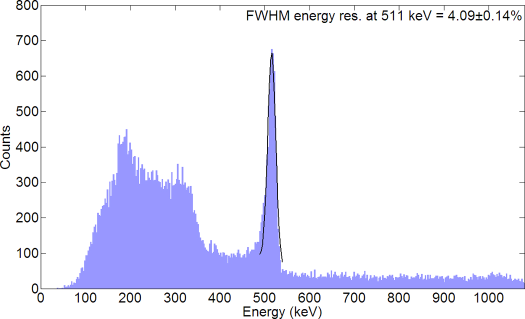
Raw energy spectrum of single anode near the detector centre for an uncollimated 22Na photon source irradiating the detector edge (at all depths). The 1275 keV photopeak is not shown as it was beyond the input dynamic range of the ADC for the selected RENA-3 gain setting. Error bar on FWHM energy resolution value corresponds to the value’s standard deviation based on Gaussian fits applied to separate anode spectra (n = 5).
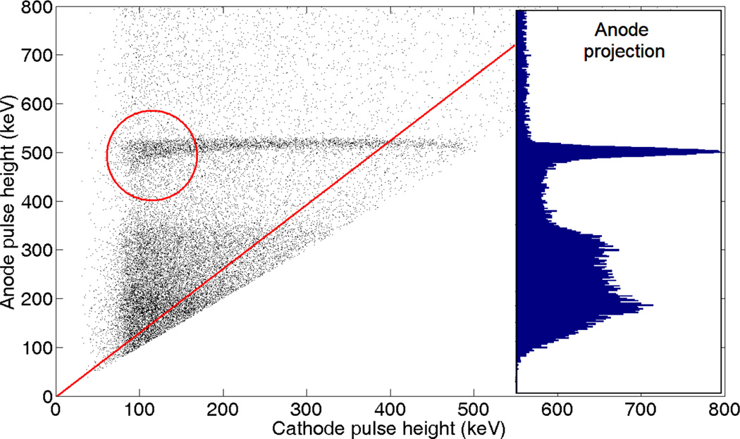
The scatter plot of figure 10 was generated to aid visualization of the origin of spectral tailing seen in figure 9, the circle highlights the events responsible. Here each event is represented by a point at a position corresponding to the event’s induced cathode (horizontal axis) and anode (vertical axis) signal amplitudes. If for each energy interval on the anode axis a horizontal bar is drawn whose length is proportional to the number of events falling within that energy interval, then we recover the familiar histogram energy spectrum as shown by figure 10’s inset.
Figure 10.
Cathode-anode signal scatter plot for an uncollimated 22Na photon source irradiating the detector edge (at all depths). Events shown have C/A ratio between 0 and 1. The circled region highlights the events that contribute to low energy tailing of the photopeak due to reverse-polarity signal contribution from holes near the anode plane. The right inset spectrum corresponds to the result of collapsing all cathode signals onto the anode axis. The diagonal line shows the locus of all interactions with a cathode-to-anode signal amplitude ratio of 0.76 (see section 6.1).
The energy spectrum of figure 9 as it appears after tailing correction due to depth-dependent signal deficit is shown in figure 12. The two spectra are based on an identical set of events but the energy resolution at 511 keV in figure 12 is 3.90±0.19%.
Figure 12.
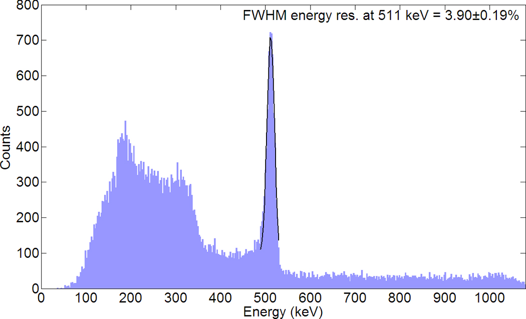
Single anode energy spectrum corrected for depth-dependent signal deficit along the DOEP for an uncollimated 22Na photon source irradiating the detector edge (at all depths). The 1275 keV photopeak is not shown due to ADC saturation. Error bar on FWHM energy resolution value corresponds to the value’s standard deviation based on Gaussian fits applied to separate anode spectra (n = 5).
The clustering pattern of events in figure 10 is to a large degree determined by the weighting potential profiles of the anode and cathode strips. The weighing potential is a normalized scalar function that quantifies the electrode’s sensitivity to space charge at all positions within the detector volume. The weighting potential is a continuous function whose value varies with spatial position, and is determined completely by the electrode and detector geometries, i.e. it is independent of detector bias voltage and detector material.
Figure 11(a) plots the weighting potential value as a function of distance from the axis of a 100 µm width anode strip (x) and the DOEP position (z). Figure 11(b) shows the corresponding contours of the weighting potential surface, where a fixed quantity of charge placed anywhere along a contour would induce a constant amount of charge on the electrode, the amount of induced charge being higher for red contours (high sensitivity, i.e. value close to 1) and lower for blue contours (low sensitivity, i.e. value close to 0).
Figure 11.
Subplot (a) shows the weighting potential profile of a 100 µm wide anode as a function of distance from the anode axis in the direction transverse to the anode pitch and the DOEP position. The lobe centred on the anode axis corresponds to the region of high charge sensitivity within the detector for the anode. Subplot (b) shows the surface’s corresponding contour plot.
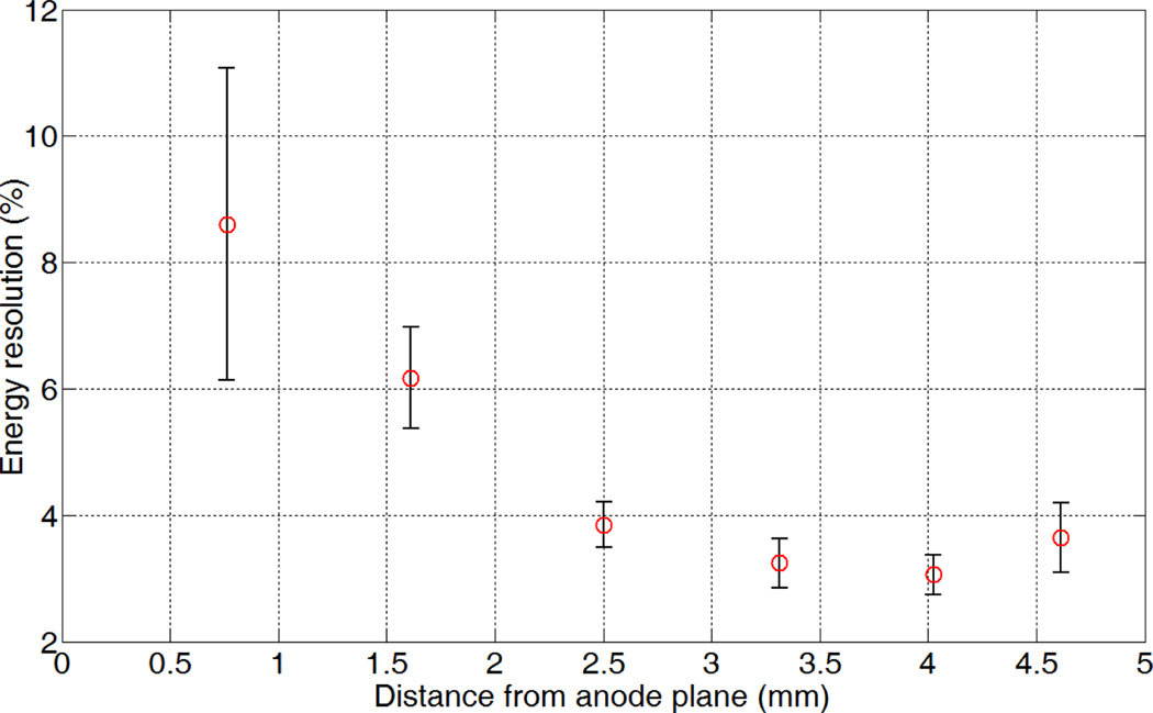
Experimental results of the detector’s spatial resolution along the direction orthogonal to the electrode planes (DOEP) (presented in section 5.3) allow one to estimate an interaction’s location along the DOEP given its C/A ratio. Hence we were able to decompose the anode energy spectrum of figure 12 into its constituent spectra each containing only interactions at a specific depth along the DOEP. Figure 13 shows the result by plotting the detector’s FWHM energy resolution performance at 511 keV as a function of photon interactions’ DOEP position. The position bins are centred at approximately 0.76 mm, 1.61 mm, 2.50 mm, 3.32 mm, 4.02 mm and 4.61 mm from the anode plane (derived from C/A ratio bins). Figure 14 shows the energy spectrum taken along the diagonal line in figure 10, which corresponds to photon interactions occurring 4.02 mm away from the anode plane. It also corresponds to the data point at 4.02 mm along the horizontal axis in figure 13.
Figure 13.
FWHM energy resolution at 511 keV of a single typical anode strip as a function of photon interaction DOEP position relative to the anode plane. The error bars denote the 95% confidence interval of the fitted energy resolution values.
Figure 14.
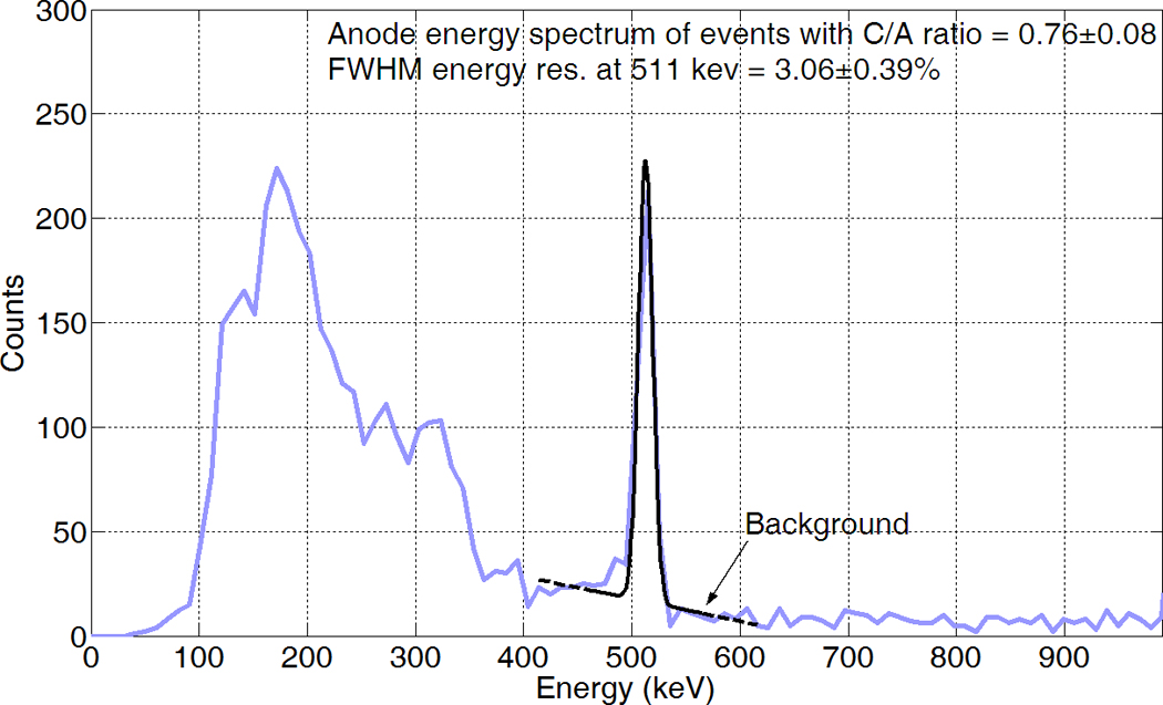
Single anode energy spectrum of photon interactions with C/A ratio of 0.76±0.08 (one depth), as derived from taking a slice cross-section through figure 10 along the diagonal line. This spectrum corresponds to the data point at 4.02 mm in figure 13. The 1275 keV photopeak is not shown due to ADC saturation, and the error bar corresponds to the 95% confidence interval of the fitted parameters.
Figure 15 shows spectra containing (a) single and (b) both single and multiple-anode events that occurred approximately 3 mm from the anode plane. For figure 15(a) the single anode triggered can be any one of the anodes read out from the detector, similarly for figure 15(b) the up to two anodes triggered can be any one or any two anodes read out. Gain and offset corrections were applied to each anode before summing anode signals (section 4.2).
Figure 15.
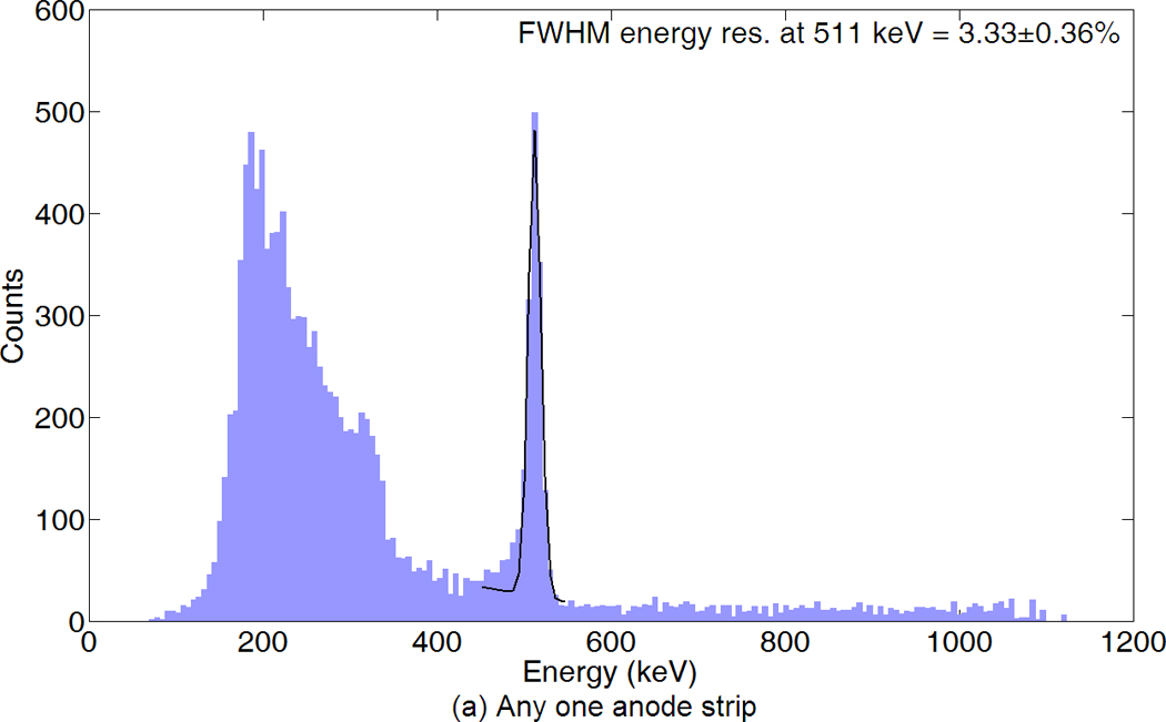
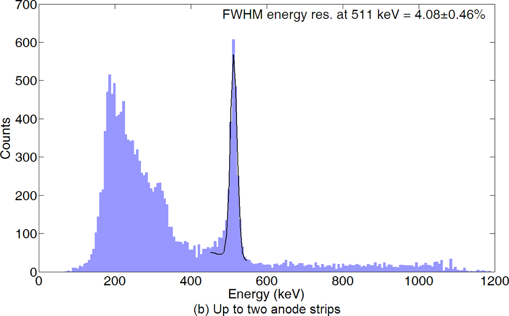
Anode energy spectrum of photon interactions 3 mm (C/A ratio = 0.53) from the anode plane where the total energy per event is summed over (a) any one or (b) up to two anode strip signals. An uncollimated 22Na source was used to irradiate the edge of the 5 mm thick detector. The spectra have been corrected for depth-dependent signal deficit along the DOEP, and the error bar corresponds to the 95% confidence interval of the fitted parameters.
Figure 16 shows the energy resolution of single and multiple-anode events as a function of the photon interaction depth. Note that whereas figure 13 is plotted for one specific anode, the “Any 1 anode” data points of figure 16 are plotted from spectra of single anode events that triggered any one of the detector’s anodes.
Figure 16.
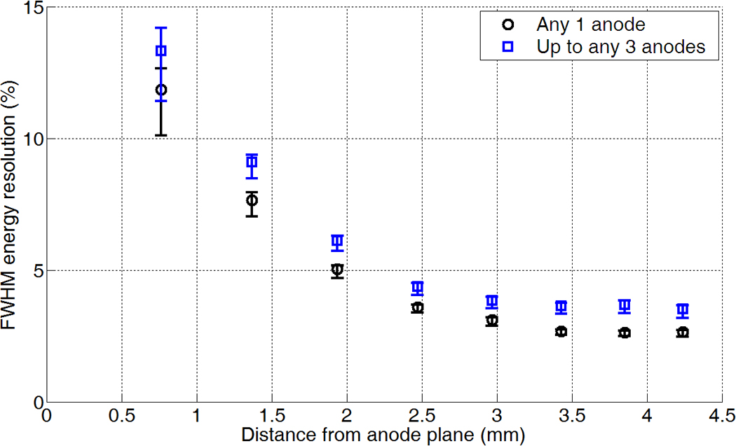
FWHM energy resolution at 511 keV for any anode strip or set of up to 3 anode strips as a function of photon interaction DOEP position relative to the anode plane for edge-on irradiation. The error bars denote the 95% confidence interval of the fitted energy resolution value. “Any 1 anode” refers to the spectrum where each event triggered exactly one and any one of the detector’s anodes; “up to any 3 anodes” refers to the spectrum where the total energy of each event was summed from up to three anode signals.
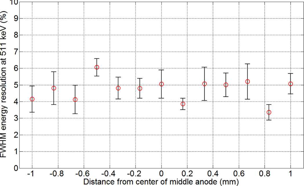
Figure 17 plots the anode FWHM photopeak energy resolution at 511 keV as a function of the collimated beam position, i.e. interaction position transverse to the anode strips (experimental setup of figure 6). The plot reflects energy resolution after correction for depth-dependent signal deficit along the DOEP. Note that positions −1 mm, 0 mm and 1 mm correspond to centres of anodes, thus the anode strip boundaries are at −0.5 mm and 0.5 mm. As was the case for figure 15 and figure 16, calibration for gain and offset variations across anodes was applied in deriving neighbour-summed energy resolution at anode strip boundaries in figure 17.
Figure 17.
Depth-corrected FWHM photopeak energy resolution at 511 keV as a function of photon interaction position transverse to the anode strips for a collimated beam stepped across 3 consecutive anode strips (located at −1 mm, 0 mm, and 1 mm, respectively). The photons were electronically collimated, and the error bar corresponds to the 90% confidence interval of the fitted parameters.
5.2. Efficacy of steering electrodes
Figure 18 shows the charge collection behaviour as a function of both i) collimated beam position transverse to the anode strips and ii) steering electrode bias voltage (each coloured line corresponds to a distinct bias value). The vertical axis is the count of events whose energy deposition fell within the energy window, i.e. if a single anode photon interaction (or a charge-shared event) has signal (or neighbour-summed signal) falling within the energy window, then the event count is incremented by 1 for that beam position. Figure 18(a) and figure 18(b) correspond, respectively, to two different energy windows widths of 662 keV±14% and 662 keV±4%. The lines in figure 18 therefore reflect the relative sensitivity of the detector across anode pitches.
Figure 18.
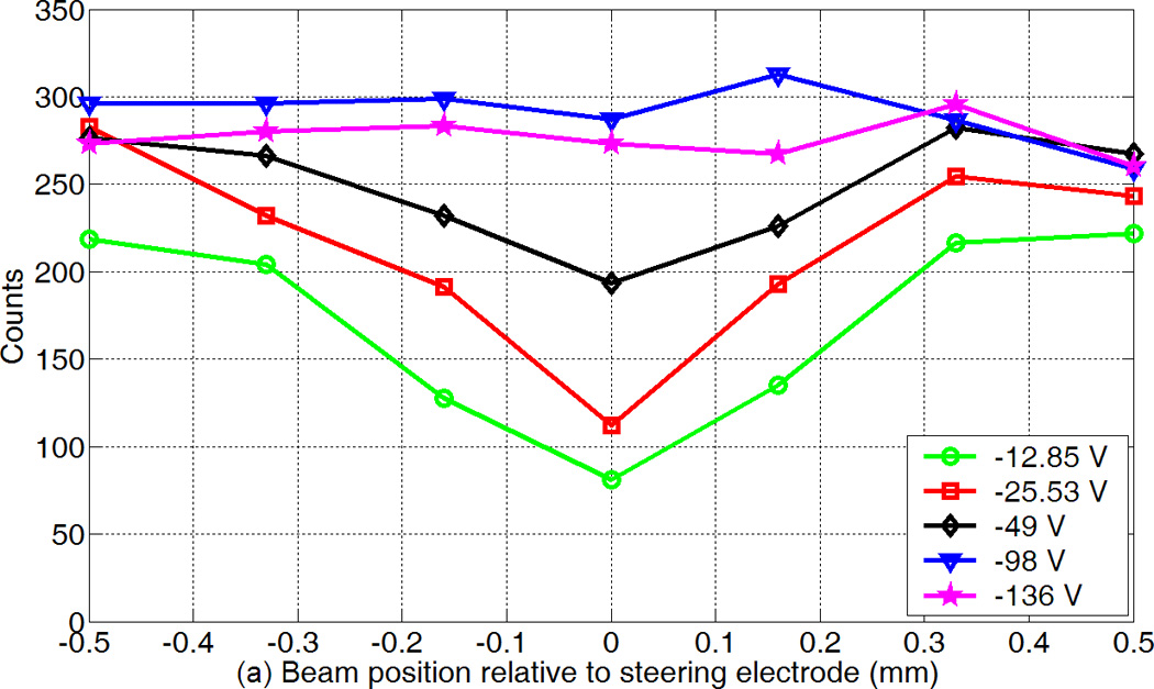
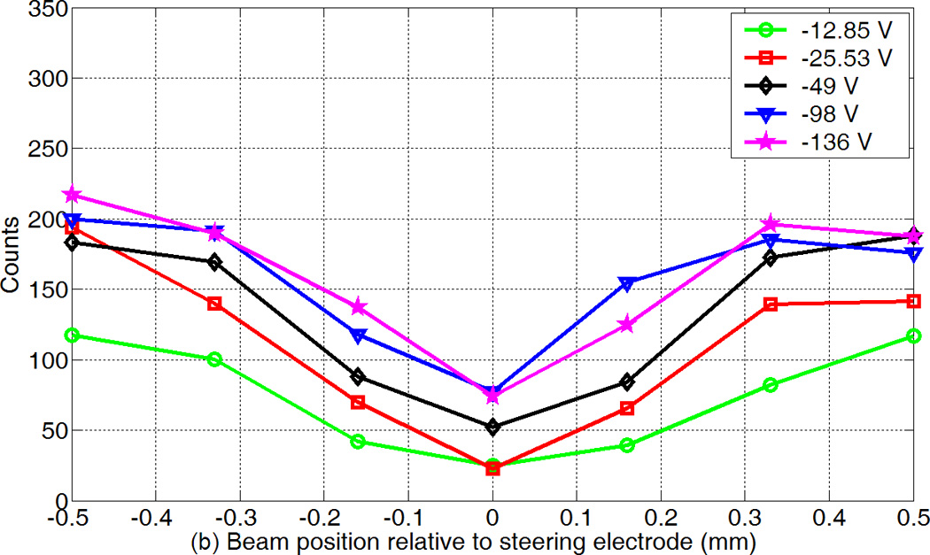
Anode charge collection behaviour for different steering electrode biases analysed with a 662 keV±14% energy window (a) and a 662 keV±4% energy window (b). The steering electrode is centred at the 0 mm position, the two adjacent anode strip centres correspond to ±0.5 mm from the steering electrode centre. Data was collected using a collimated beam orthogonal to and incident upon the cathode plane stepped in between two anodes.
5.3. Spatial resolution along the direction orthogonal to the electrode planes (DOEP)
Using the experimental setup and protocol described in section 4.4, the distribution of C/A values for each collimated beam position between the cathode and anode planes is shown in figure 19. The markers denote the mean of C/A ratio for 12 collimated beam positions and the error bars show the extent of the corresponding distribution’s FWHM. Figure 20(a) exhibits a selected subset of the data points in figure 19 (black circles) that are spaced 1 mm apart as observed looking along the direction of the beam position axis in figure 19. Similarly figure 20(b) shows a subset of the data points in figure 19 (red squares) that are spaced 0.5 mm apart in the same projection as figure 20(a). The heights of the fitted Gaussian curves are normalised to facilitate comparison. Since the black circles show only measurements at 1 mm intervals starting at 1 mm from the anode plane, the measurements at the blue triangles are included in figure 19 to illustrate that the C/A trend holds even within that first 1 mm from the anode plane. The first and second blue triangles from the left are at 330 µm and 660 µm from the anode plane respectively.
Figure 19.
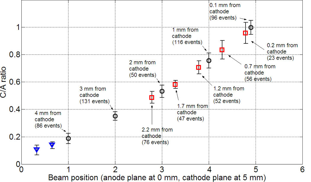
C/A ratio as a function of collimated beam position irradiating edge-on between the anode and cathode planes. The error bars denote the extent of the FWHM for each data point; markers denote the mean values and are colour-coded black (circles, 1 mm spacing) and red (squares, 0.5 mm spacing) to the corresponding data points in figure 20. Blue triangles illustrate C/A values within the first 1 mm from the anode plane at 330 µm and 660 µm.
Figure 20.
C/A ratio distribution for beam positions separated by (a) 1 mm along the DOEP (black circles in figure 19) and by (b) 0.5 mm along the DOEP (red squares in figure 19).
The R2 errors of the fitted Gaussian curves in figure 20 are given in table 1:
Table 1.
R-squared error of fitted Gaussian curves in figure 20.
| Distance from cathode plane (subplot a) (mm) |
R2 error | Distance from cathode plane (subplot b) (mm) |
R2 error |
|---|---|---|---|
| 0.1 | 0.9358 | 0.2 | 0.9561 |
| 1.0 | 0.9251 | 0.7 | 0.8951 |
| 2.0 | 0.9348 | 1.2 | 0.9434 |
| 3.0 | 0.9511 | 1.7 | 0.9690 |
| 4.0 | 0.9627 | 2.2 | 0.9630 |
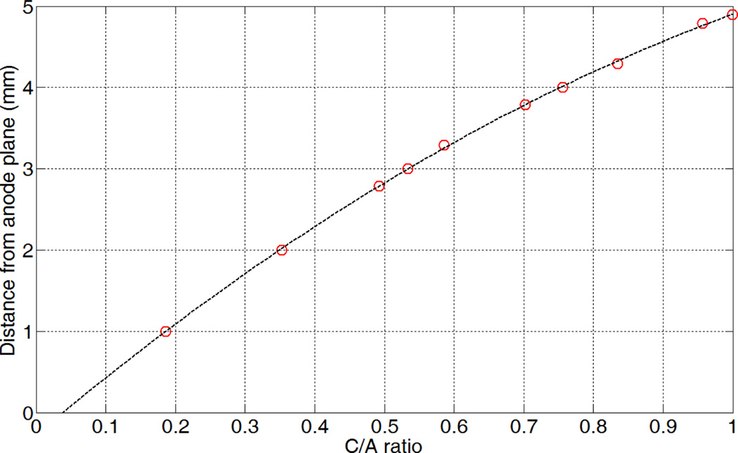
Knowing the precise DOEP position of the collimated beam as well as the corresponding Gaussian-fitted mean C/A ratio values allows one to find the inverse mapping. Figure 21 shows the C/A ratio-to-DOEP position mapping found by fitting a quadratic polynomial to the data in figure 20. This mapping is referred to in section 5.1 where it was used to plot the energy resolution vs. DOEP position relationship (figure 13 and figure 16).
Figure 21.
Quadratic model of a photon interaction’s true DOEP position as a function of its C/A ratio (R2 error = 0.9997). The circles’ horizontal position denotes the mean C/A ratio (found by Gaussian curve fitting) corresponding to the collimated beam’s DOEP position as represented by the circles’ vertical position.
5.4. Anode spatial resolution
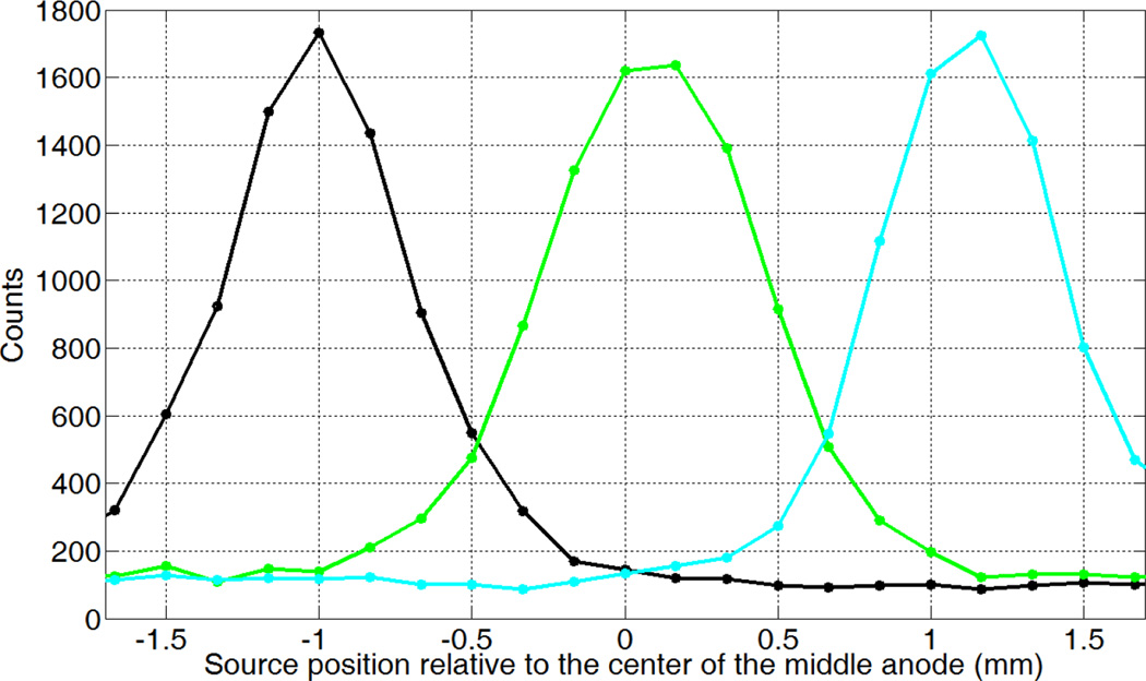
The coincident event count response obtained from pairs of anodes facing each other across the 40 mm gap (see figure 6) is as shown in figure 22. The horizontal axis shows the source position and the vertical axis is the normalised number of coincident events detected on each opposing anode pair (represented by different colour lines) for a given source position. Across these centre anodes, the PSF was 0.78±0.10 mm FWHM including the 250 µm diameter of the point source.
Figure 22.
Coincidence point spread function across 3 anode strips for a 22Na photon source electronically collimated to incident upon the detector edge. The curves show how the number of coincident events detected in each pair of opposite-facing anodes (denoted by different colours) rise and fall as the source is moved along the centre line between detectors (see figure 6).
6. Discussion
6.1. Anode energy resolution
Hole trapping is significant within CZT detectors since the hole mobility in CZT is about 20 times lower than electron mobility (Erickson et al 2000). Slowly-moving and trapped holes induce a signal component on anodes that is opposite in polarity to electrons, resulting in anode signal deficit. The effects of trapped holes beyond the immediate vicinity of anodes can be mitigated by the small-pixel effect.
The small-pixel effect is brought about by the small width of the anode, which causes the region of high sensitivity to space charge to be restricted to the immediate vicinity of the anode as reflected by the sharp lobe shown in figure 11(a) (Ramos 1939, Barrett et al 1995, Luke 1996, Eskin et al 1999, Kalemci et al 1999). The effectiveness of the small-pixel effect is evident through the locus of 511 keV event cluster in the scatter plot of figure 10, which is essentially horizontal and forms a band of approximately uniform variance. The slight downward curvature of the photopeak band at large cathode signal values is attributable to signal deficit due to trapping of drifting electrons for photon interactions far from the anode plane.
The photopeak tailing seen in figure 9 is attributable to the downward curvature and the increase in variance of the event distribution in the photopeak at small cathode signal values (events highlighted by the circle in figure 10). These events correspond to interactions very close to the anode plane, where after the electrons of a photon interaction have drifted away the holes can remain in the vicinity of the anode strips longer than the pulse peaking time. The prolonged presence of holes near anode strips creates a reverse-polarity induction on the anodes, since the small-pixel is no longer effective in this range.
The variation of FWHM energy resolution at 511 keV across the detector’s 5 mm DOEP thickness (z axis in figure 2) was investigated with the aid of the C/A ratio-to-DOEP position mapping of figure 21 (see section 6.3 for related discussion). The result is shown in figure 13. The spectra from which the data points in figure 13 were derived can be visualised as slice cross-sections of figure 10 taken along straight lines through the origin whose slope is the inverse of C/A ratio of interest. For example figure 14 shows the spectrum corresponding to the slice along the diagonal line in figure 10 (C/A ratio = 0.76), for which the FWHM energy resolution at 511 keV is 3.06±0.39%.
Figure 13 shows that the small-pixel effect helps to maintain an approximately uniform energy resolution across most of the detector’s 5 mm thickness, but the energy resolution for a single anode in fact spans a range from 3.05% at 4.02 mm from the anode plane to 8.60% at 0.76 mm from the anode plane. Along with figure 10, this illustrates that both the photopeak’s position (signal deficit) as well as its width (energy resolution at a particular DOEP position) vary with the DOEP position, and it is only in the aggregate (over all DOEP positions) that the detector exhibits the 4.09% energy resolution of figure 9.
Seeing that the photopeak position and width both vary systematically as a function of interaction depth (DOEP), which can be estimated with better than 1 mm precision (refer to section 6.3 for discussion on DOEP resolution), both effects may be addressed using the C/A ratio. In particular equation (1) was used to correct for the shift in photopeak position due to signal deficit induced by holes near the anode plane, figure 12 shows the energy spectrum of figure 9 (4.09±0.19% energy resolution) after the correction (3.90±0.19% energy resolution).
Similarly, depth gating based on the DOEP position will be used to address the depth-dependent photopeak width, so that the appropriate energy gating settings can be chosen for each photon interaction based on the energy resolution at the interaction’s DOEP position.
The single-anode event specrtum and energy resolution shown in figure 15 and figure 16 differ from those of figure 12 and figure 13 in that whereas the latter are based on one specific anode, the former are based on single-anode events that could have triggered any one of the detector’s anodes read out. Figure 16 shows that the range of energy resolution for single and multiple-anode events are 2.65%–11.85% and 3.25%–13.31%, respectively. This slight degradation of resolution seen in figure 15 and figure 16 for multiple-anode events is unsurprising since the signal variance due to independent noise contribution from each individual RENA-3 channel adds in quadrature. Another factor degrading the energy resolution in this case is the signal deficit due to low hole mobility, which is magnified for charge-shared interactions near the anode plane. In this case the reverse-polarity induction on each anode comes from the full population of holes generated by an interaction that remains in the vicinity of the anode plane past the pulse peaking time, but the electron signal component comes from only the fraction of electrons collected by that anode. This asymmetry in signal contribution increases the amount of signal deficit, and in turn the photopeak tailing towards low energies in the spectrum containing multiple-anode events.
As for anode energy resolution as a function of photon interaction position transverse to the anode strips within one anode pitch, figure 17 demonstrates that there is no drastic change in FWHM energy resolution at 511 keV as the electronically collimated slit beam is scanned across the detector’s edge-face. The relatively constant FWHM energy resolution (~5% on average) confirms that in spite of the spatial pixel decomposition of the CZT detector volume by anodes and steering electrodes, the device can continue to operate as a continuous detector with uniform energy resolution performance throughout.
It is expected that these energy resolution results can be improved since they were based on measurements made with a prototype system that was not optimised for low electronic noise. Nevertheless, current results suffice in demonstrating that CZT is capable of providing excellent energy resolution for PET.
6.2. Efficacy of steering electrodes
The lines of figure 18 reflect relative photon sensitivity across one anode pitch as explained in section 5.2. Using a sum-energy window of 662 keV±14%, figure 18(a) shows that the photon sensitivity increases across the entire anode pitch with increasing steering bias. This verifies that when biased at a more negative potential compared to the anode strips the steering electrodes are more effective at repelling electrons towards the anodes. The photon sensitivity profile across the anode pitch also appears approximately uniform beyond about −100 V of steering bias, at which point the number of photon interactions with near-complete charge collection becomes an approximately constant function of the interaction position.
When a narrower sum-energy window of 662 keV±4% was used (figure 18(b)), the sensitivity profile displays clear peaks and a valley, which is centred on the steering electrode and remains visible even at high steering bias values. This indicates that more photon interactions fall outside of the nominal photopeak energy range when they occur near the centre of a steering electrode. This is likely due to the occurrence of small amounts of charge loss to non-metalized areas on the detector face between the narrow anode strips and the steering electrode, resulting in a charge falling just outside the photopeak i.e. not falling in the 662 keV±4% window, but falling in the 662 keV±14% window. Nevertheless, the photon sensitivity increases with increasing steering bias in figure 18(b), but only up to approximately −100 V, after that there is no increase and the valley remains.
These results verify the efficacy of steering electrode in enhancing the detector sensitivity by mitigating charge loss, but they also reveal sub-pitch-scale variations in the detector’s capability for complete charge collection. The sub-pitch variations (the sensitivity dips over steering electrodes) will be corrected during the detector efficiency normalization procedure of image reconstruction.
6.3. Spatial resolution along the direction orthogonal to the electrode planes (DOEP)
Two important observations can be made from figure 19 and figure 20(a). Firstly, it is clear that the variation in the mean of the C/A ratio is almost linear with position of photon interaction along the DOEP. It should be noted that this does not hold for semiconductor detectors in general e.g. Si or Ge, instead it is a fortuitous result of a number of factors. Firstly, as mentioned above CZT has very different mean drift length values for electrons and holes so that hole trapping is significant within the detector. Secondly, in spite of hole trapping, the small-pixel effect causes the anode signal to be essentially proportional to the photon interaction energy. Finally, due to their larger widths the cathodes do not exhibit the small-pixel effect i.e. the weighting potential lobe rolls off slowly in figure 11(a), so that trapped holes cause the cathode signal to be proportional to the product of photon interaction energy and the DOEP position. The net effect of these factors is that the C/A ratio is approximately linearly proportional to the DOEP position.
This linearity suggests a simple model for inferring the position of a photon interaction along the DOEP based on an interaction’s C/A ratio. Figure 21 shows how this inverse relationship of true DOEP position as function of C/A ratio can be captured using a simple quadratic polynomial. The polynomial was optimally fitted in the least squared error sense with an R2 error value of 0.9997, and enables estimation of an event’s true DOEP position if its C/A ratio is known e.g. used in converting the energy resolution as a function of C/A ratio to a function of the true DOEP position (section 6.1).
Secondly, we see from the fitted Gaussian curves that the spread of the C/A ratio in each position is sufficiently tight to allow positions 1 mm apart to be resolved. In fact, across the 5 Gaussian curves fitted to C/A ratio distributions for pencil-beam-collimated photon interactions positioned 1 mm apart along the DOEP (figure 20(a)), the FWHM of the fitted curves is 0.44±0.07 mm. This tells us that we can readily achieve 1 mm resolution along the DOEP, so the desired voxel size of 1 mm × 1 mm × 5 mm for the high-resolution small animal PET system can be realised.
A subset of figure 19’s data points that are spaced 0.5 mm apart are plotted in figure 20(b). Judging by the R2 error values of table 1, the fitted parameters account reasonably well for the data points’ Gaussian distribution. Note that the left-most three fitted Gaussian lobes in figure 20(b) intersect below the half-maximum level, while the right-most two lobes intersect above or approximately at the half-maximum level. The inconclusiveness of this result is attributable to the poorer statistics of data points of figure 20(b) than those of figure 20(a), but it is consistent with previous results of 0.44±0.07 mm FWHM resolution since 0.5 mm falls within this range. The finding is promising as it points to the system’s potential of achieving 0.5 mm resolution along the DOEP. In fact, if the data are collected in list mode, the C/A ratio enables selectable DOEP resolution as determined by the choice of bin size along that direction.
6.4. Anode spatial resolution
Figure 22 shows that a clear margin exists between the half-maximum level and the level at which the curves intersect. The point spread function curves shown include the contribution from the finite size of the 250 µm diameter 22Na point source used. The anodes are therefore well-resolved as the source is stepped across the detector face, confirming that the 1 mm anode pitch enables ≤1 mm FWHM spatial resolution along that direction.
6.5. PET imaging with CZT and future work
Compared to scintillation detectors commonly used in PET systems, the preceding energy and spatial resolution results verify that CZT can offer superior 511 keV photopeak energy resolution (~3% vs. ~15% FWHM) and comparable effective detector voxel size needed for 1 mm3 resolution PET imaging (1 mm × 1 mm × 5 mm). The small detector voxels allow for narrow lines or tubes of response for high resolution image reconstruction, and given the detector arrangement of figure 1, the CZT detector’s 3-D positioning capability also provides precise depth of interaction information, which reduces parallax error. These translate to not only high resolution but also improved resolution uniformity throughout the FOV.
CZT’s high energy resolution presents an opportunity to further enhance the system sensitivity by utilizing multiple interaction photon events in PET imaging. In particular, by using the position, energy and time measurements of the individual photon interactions in a multiple interaction photon event, Bayesian estimation can be applied to identify the initial photon interaction based on Compton kinematics and CZT’s Klein–Nishina differential cross section. The position of the initial photon interaction in turn determines the positioning of the event’s LOR; PET imaging utilizing multiple interaction photon events has been seen to improve the contrast-to-noise ratio of reconstructed images (Gu et al 2010). CZT would be preferred in this context over scintillation detectors, since the accuracy of Bayesian estimation correlates with the detector energy resolution i.e. increasing with more accurate measurements of interaction energy (Pratx and Levin 2009).
Unlike its scintillation crystal counterpart, small voxels within a CZT detector crystal also has no associated dead area between them because of e.g. reflector material, air gaps, or photodetector dead area. This serves to enhance the packing fraction (and hence system sensitivity) as well as sensitivity uniformity throughout the detector volume (Habte et al 2007). In fact the system can achieve coincidence sensitivity as high as ~20% for a point source at the centre of the FOV (Levin et al 2006), which is an order of magnitude higher than reported for high-resolution PET systems based on other detector technologies (Missimer et al 2004, Yang et al 2004, Vaska et al 2005a, Sempere Roldan 2007, Spanoudaki et al 2007, Bergeron et al 2009). For a given injected dose or a fixed scan time, the CZT system is therefore expected to yield images with improved statistics and signal-to-noise ratio performance.
In future work, studies will focus on potential methods for improvements in energy resolution, and schemes to achieve sub-electrode-pitch spatial resolution. Although the timing performance of a large volume CZT detector as presented is expected to be poorer than that of scintillation crystals, prior study suggests that at fixed activity and for events in the photopeak, CZT’s high energy resolution can effectively compensate for its poorer timing by reducing the effects of single photons that undergo scatter on the randoms fraction (Levin et al 2006). Nevertheless, prospective studies will also investigate methods to obtain accurate time pick-off for single photon events in CZT.
7. Conclusion
CZT has numerous properties that make it attractive as a photon detector in PET applications. This work focused on assessing the detector performance for a prototype detector system comprising two 40 mm × 40 mm × 5 mm monolithic CZT crystal detectors. The raw single anode event energy resolution at 511 keV was measured to vary monotonically with the photon interaction depth, ranging from 3.06±0.39% to 8.58±3.05%; a 3.90±0.19% FWHM energy resolution was measured with the RENA-3 ASIC when no depth gating is applied. Similarly, FWHM energy resolution ranged from 3.25% to 13.31% for multiple-anode events. The study also established the efficacy of steering electrodes, in particular, full charge collection among anodes was achieved for steering bias voltage lower than −100 V with reference to the anode potential. In terms of spatial resolution, 1 mm resolution in the direction orthogonal to the electrode planes was verified to be readily achievable, while an anode resolution of 1 mm was observed using electronic collimation. Overall, the system-level metrics show that this detector is capable of providing excellent performance and shows great promise for development into a full small animal PET imaging system.
Acknowledgements
This work was supported by the U.S. National Institute of Health under Grant No. R01 CA120474.
References
- Barrett HH, Eskin JD, Barber HB. Charge Transport in Arrays of Semiconductor Gamma-Ray Detectors. Phys. Rev. Lett. 1995;75:156–159. doi: 10.1103/PhysRevLett.75.156. [DOI] [PubMed] [Google Scholar]
- Bergeron M, Cadorette J, Beaudoin JF, Lepage MD, Robert G, Selivanov V, Tetrault MA, Viscogliosi N, Norenberg JP, Fontaine R, Lecomte R. Performance Evaluation of the LabPET APD-Based Digital PET Scanner. IEEE Transactions on Nuclear Science. 2009;56:10–16. [Google Scholar]
- Erickson JC, Yao HW, James RB, Hermon H, Greaves M. Time of Flight Experimental Studies of CdZnTe Radiation Detectors. Journal of Electronic Materials. 2000;29:699–703. [Google Scholar]
- Eskin JD, Barrett HH, Barber HB. Signals Induced in Semiconductor Gamma-Ray Imaging Detectors. J. Appl. Phys. 1999;85:647–659. [Google Scholar]
- Gu Y, Pratx G, Lau FWY, Levin CS. Effects of Multiple-Interaction Photon Events in a High-Resolution PET System that Uses 3-D Positioning Detectors. Medical Physics. 2010;37:5494–5508. doi: 10.1118/1.3483262. [DOI] [PMC free article] [PubMed] [Google Scholar]
- Habte F, Foudray AMK, Olcott PD, Levin CS. Effects of System Geometry and Other Physical Factors on Photon Sensitivity of High-resolution Positron Emission Tomography. Physics in Medicine and Biology. 2007;52:3753–3572. doi: 10.1088/0031-9155/52/13/007. [DOI] [PMC free article] [PubMed] [Google Scholar]
- Hong J, Bellm E, Grindlay J, Narita T. Cathode Depth Sensing in CZT Detectors. Proc. SPIE. 2003;5165:54–62. [Google Scholar]
- Kalemci E, Matteson JL, Skelton RT, Hink PL, Slavis KR. Model Calculations of the Response of CZT Strip Detectors. Hard X-Ray/Gamma-Ray and Neutron Optics, Sensors and Applications, Proc. SPIE. 1999;3768:360–373. [Google Scholar]
- Levin CS, et al. Promising Characteristics and Performance of Cadmium Zinc Telluride Detectors for Positron Emission Tomography; IEEE Nuclear Science Symposium Medical Imaging Conference Book of Abstracts; 2004a. [Google Scholar]
- Levin CS, Habte F, Foudray AMK. Methods to Extract More Light from Minute Scintillation Crystals Used in an Ultra-High Resolution Positron Emission Tomography Detector. Nuclear Instruments and Methods in Physics Research Section A. 2004b;527:35–40. [Google Scholar]
- Levin CS, Foudray AMK, Habte F. Impact of High Energy Resolution Detectors on the Performance of a PET System Dedicated to Breast Cancer Imaging. Physica Medica. 2006;21 suppl. 1:28–34. doi: 10.1016/S1120-1797(06)80020-7. [DOI] [PubMed] [Google Scholar]
- Levin CS. New Imaging Technologies to Enhance the Molecular Sensitivity of Positron Emission Tomography. Proceedings of the IEEE. 2008;96:439–467. [Google Scholar]
- Li W, He Z, Knoll GF, Wehe DK, Du YF. A Modeling Method to Calibrate the Interaction Depth in 3-D Position Sensitive CdZnTe Gamma-Ray Spectrometers. IEEE Transactions on Nuclear Science. 2000;47:890–894. [Google Scholar]
- Luke PN. Electrode Configuration and Energy Resolution in Gamma-Ray Detectors. Nuclear Instruments and Methods in Physics Research Section A. 1996;380:232–237. [Google Scholar]
- Mashlum G, Dietzel K, Meier D, Szawlowski M, Sundal B, Vandehei T, Wagenaar D, Patt BE. Study of Cadmium Zinc Telluride (CZT) Radiation Detector Modules under Moderate and Long-term Variations of Temperature and Humidity; IEEE Nuclear Science Symposium Conference Record; 2007. pp. 1645–1648. [Google Scholar]
- Matteson JL, Pelling MR, Skelton RT. CZT Detectors with 3-D Readout for Gamma-Ray Spectroscopy and Imaging. Proc. SPIE. 2002;4784:1–13. [Google Scholar]
- Matteson JL, Gu Y, Skelton RT, Deal AC, Stephan EA, Duttweiler F, Huszar GL, Gasaway TM, Levin CS. Charge Collection Studies of a High Resolution CZT-Based Detector for PET; IEEE Nuclear Science Symposium Conference Record; 2008. pp. 503–510. [Google Scholar]
- Missimer J, Madi Z, Honer M, Keller C, Schubiger A, Ametamey SM. Performance Evaluation of the 16-module Quad-HIDAC Small Animal PET Camera. Physics in Medicine and Biology. 2004;49:2069–2081. doi: 10.1088/0031-9155/49/10/016. [DOI] [PubMed] [Google Scholar]
- Mitchell GS, Sinha S, Stickel JR, Bowen SL, Cirignano LJ, Dokhale P, Kim H, Shah KS, Cherry SR. CdTe Strip Detector Characterization for High Resolution Small Animal. PET IEEE Transactions on Nuclear Science. 2008;55:870–876. [Google Scholar]
- Morimoto Y, et al. Development of a Prototype 3D PET Scanner Using Semiconductor Detectors and Depth of Interaction Information. In: Tamaki N, Kuge Y, editors. Molecular Imaging for Integrated Medical Therapy and Drug Development. Tokyo: Springer; 2010. pp. 30–41. [Google Scholar]
- Pratx G, Levin CS. Bayesian Reconstruction of Photon Interaction Sequences for High-Resolution PET Detectors. Physics in Medicine and Biology. 2009;54:5073–5094. doi: 10.1088/0031-9155/54/17/001. [DOI] [PMC free article] [PubMed] [Google Scholar]
- Ramo S. Currents Induced by Electron Motion. Proceedings of the I.R.E. 1939;27:584–585. [Google Scholar]
- Sempere Roldan P. Raytest ClearPET™, A New Generation Small Animal PET Scanner. Nuclear Instruments and Methods in Physics Research Section A. 2007;571:498–501. [Google Scholar]
- Spanoudaki V, Torres-Espallardo I, Rafecas M, Ziegler S. Performance Evaluation of MADPET-II, A Small Animal Dual Layer LSO-APD PET Scanner with Individual Detector Read Out and Depth of Interaction Information. Journal of Nuclear Medicine. 2007;48 suppl. 2:131. [Google Scholar]
- Vaska P, et al. Initial Performance of the RatCAP, a PET Camera for Conscious Rat Brain Imaging; IEEE Nuclear Science Symposium Conference Record; 2005a. pp. 3040–3044. [Google Scholar]
- Vaska P, Bolotnikov A, Carini G, Camarda G, Pratte JF, Dilmanian FA, Park SJ, James RB. Studies of CZT for PET Applications; IEEE Nuclear Science Symposium Conference Record; 2005b. pp. 2799–2802. [Google Scholar]
- Yang Y, Tai YC, Siegel S, Newport DF, Bai B, Li Q, Leahy RM, Cherry SR. Optimization and Performance Evaluation of the MicroPET II Scanner for In Vivo Small-Animal Imaging. Physics in Medicine and Biology. 2004;49:2527–2545. doi: 10.1088/0031-9155/49/12/005. [DOI] [PubMed] [Google Scholar]
- Zhang F, Zhong H, Xu D, Meng LJ. Feasibility Study of Using Two 3-D Position Sensitive CZT Detectors for Small Animal PET; IEEE Nuclear Science Symposium Conference Record; 2005. pp. 1582–1585. [Google Scholar]


