Abstract
A guided-wave chemical sensor for the detection of environmental pollutants or biochemical substances has been designed. The sensor is based on an asymmetric directional coupler employing slot optical waveguides. The use of a nanometer guiding structure where optical mode is confined in a low-index region permits a very compact sensor (device area about 1200 μm2) to be realized, having the minimum detectable refractive index change as low as 10-5. Silicon-on-Insulator technology has been assumed in sensor design and a very accurate modelling procedure based on Finite Element Method and Coupled Mode Theory has been pointed out. Sensor design and optimization have allowed a very good trade-off between device length and sensitivity. Expected device sensitivity to glucose concentration change in an aqueous solution is of the order of 0.1 g/L.
Keywords: Integrated optics, Optical sensor, Slot waveguides, Silicon-on-insulator
1. Introduction
In recent years considerable research effort has been developed to employ electronic and optical micro- and nano-sensors in a great number of application fields such as medicine, microbiology, particle physics, automotive, environmental safety and defence. Sensor and actuator monolithic integration in micro-electro-mechanical systems (MEMSs) and micro-opto-electro-mechanical systems (MOEMSs) has been achieved in a large number of sensing devices. Simultaneously, photonic sensors have attracted great attention because of their immunity to electromagnetic interference, good compactness and robustness and high compatibility with fibre networks, but also due to the shorter response time and higher sensitivity and stability possible, compared to MEMS/MOEMS devices.
A number of peculiar characteristics are usually required for electronic and photonic sensors used for chemical applications, such as biomolecule concentration measurement, DNA sequencing, pH estimation, pollutant control and gas monitoring. A chemical sensor has to be contextually highly sensitive and selective to the analyte being detected, as well as immune to external disturbances such as pressure or temperature changes. Using integrated photonic technologies, it is possible to fabricate very compact, high performing and low-cost chemical and biochemical sensors [1]. Different kinds of integrated optical chemical sensors have been proposed over the years, like those based on directional couplers [2], Mach-Zehnder interferometers [3-5], Bragg gratings [6-7], micro-ring resonators [8-10], and photonic crystal micro-cavities [11]. Many of these devices have been realized adopting CMOS-compatible technological processes.
Among the CMOS-compatible technologies, Silicon-on-Insulator (SOI) is emerging as the most attractive for a wide spectrum of applications [12]. The reasons of this great interest in SOI-based integrated optics are related to the possibility to realize waveguides exhibiting low loss (less than 1 dB/cm) and high index contrast, the low cost of silicon and wide production infrastructure available for silicon based integrated device fabrication. SOI technological platform has been demonstrated as very attractive in the realization of highly compact integrated optical structures, such as micro-ring and micro-racetrack resonators [13], Bragg gratings [14], and Fabry-Perot microcavities [15].
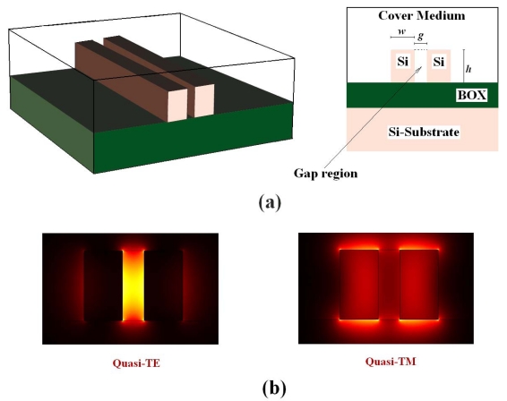
There is a current trend in SOI photonic integrated circuits and devices to move toward smaller dimensions to achieve cost efficiency and for device performance improvement. In this scenario, a silicon nanometer guiding structure, usually referred to as a slot waveguide [16], is attracting considerable attention. In optical slot waveguides, e.g. fabricated in SOI technology by either e-beam or deep-UV lithography [17], the electric field discontinuity at the interface between high index contrast materials enables high optical confinement inside a nanometer-scale area (gap region) of low-index material (e.g. air, silicon oxide, aqueous solutions, silicon nanocrystals, thermo-optic or electro-optic polymers). This guiding structure can be realized nearing two silicon wires having nanometer dimensions, as in Figure 1(a). It supports both fundamental quasi-TE and quasi-TM modes, whose typical profiles are shown in Figure 1(b). The quasi-TE mode is highly confined in the low-index gap region between the wires, whereas only about 5 % of the optical power carried out by the quasi-TM mode is localized in the gap region.
Figure 1.
(a) Slot waveguide typical structure (BOX: Buried Silicon Oxide). (b) Profiles of quasi-TE and quasi-TM modes confined in a slot waveguide.
In the last three years, a great variety of optical devices have been proposed and realized using SOI slot waveguides, including micro-ring resonators [18-20], disk resonators [21], optical micro-switches [22] and modulators [23-25], nano-mechanical photonic sensors [26], electrically pumped light emitting devices [27], directional couplers [28-29], all-optical logic gates [30], multimode interference beam splitters, wavelength demultiplexers [31-32], polarization rotators [33] and one dimensional photonic crystals [34-35].
Very recently, optical manipulation of nanoparticles and DNA molecules has been successfully demonstrated in silicon slot waveguides [36]. Consequently, the use of slot waveguides in lab-on-a-chip micro-systems is becoming more and more attractive.
The non linear properties of slot waveguides have been also investigated assuming the gap region filled by highly non linear materials, e.g. silicon nanocrystals [37-39]. Gaussian-like mode coupling into a slot waveguide has been achieved with a loss around 0.01 dB with a 100 μm long integrated device [40]. Grating couplers for SOI slot waveguides have been theoretically investigated too [41].
Alternative materials such as silicon nitride or Al0.3Ga0.7As have been recently proposed for slot guiding structures [42]. Horizontal slot waveguides have been also optimized [43], experimentally investigated [44] and employed to enhance photoluminescence of Er3+ doped Si nanoclusters in a low-index SiO2 matrix [45]. A multiple-slot guiding structure has been proposed to further enhance the optical confinement inside the slot regions [46]. To decrease the group velocity of an optical wave propagating in a slot waveguide, a silicon-based slot photonic crystal guiding structure has been proposed and demonstrated [47]. An electro-optic modulator based on a similar structure has been theoretically analyzed [48]. Finally, plasmonic slot waveguides based on a deep nanometer slot in a thin metallic film have been widely investigated for their use at visible and near infrared wavelengths [49].
The slot guiding structure effective index is very sensitive to changes in the cover medium refractive index. Adopting as cover medium an aqueous solution, whose refractive index depends on the concentration of the analyte of interest (glucose or ethanol, for example), we could observe a waveguide effective index shift due to analyte concentration changes. By monitoring the slot guiding structure effective index in an appropriate integrated architecture (e.g. Mach-Zehnder interferometer, ring resonator, Bragg grating, directional coupler, and so on), it is possible to fabricate highly sensitive and miniaturized integrated optical chemical sensors.
Slot waveguides have recently been demonstrated as very useful for chemical and biochemical optical sensing [50] and an integrated biochemical sensor (operating at 1,300 nm) based on a slot-waveguide microring resonator in Si3N4/SiO2 has been also demonstrated [51]. Highly sensitive molecular binding detection by a Si3N4/SiO2 slot waveguide has been experimentally demonstrated in [52]. Finally, a micro-ring resonator exploiting a SOI slot guiding structure has been adopted for gas sensing [53].
In this paper, we propose the use of slot waveguides to design an asymmetric directional coupler for optical chemical sensing. SOI technology has been assumed in the design at operating wavelength λ = 1,550 nm. Finite Element Method (FEM) [54] and Coupled Mode Theory (CMT) have been employed for device modelling and optimization. CMT has been previously adopted for designing symmetrical directional couplers based on SOI slot waveguides [29]. Model validation by an accurate simulation tool based on 3D EigenMode Expansion (EME) method [55] has been also performed.
2. Sensor architecture and guiding structure
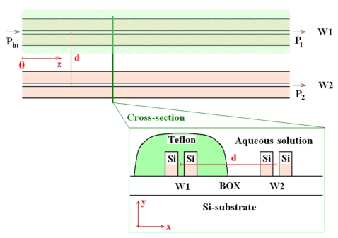
The proposed integrated sensor, whose architecture is shown in Figure 2, includes two parallel slot waveguides separated by a distance d between slot waveguide centres, then forming a directional coupler.
Figure 2.
Architecture of proposed integrated optical sensor.
This coupler is asymmetric because in one guiding structure (W1) the cover material (also filling the gap) is Teflon fluoropolymer (refractive index 1.31) whereas in the other waveguide (sensing waveguide, W2) the cover medium is constituted by an aqueous solution whose refractive index (around 1.33) depends on the concentration of the chemical agent (e.g. glucose) dispersed in the solution. In fact, a glucose concentration change of 1 g/L induces a refractive index shift in the solution of the order of 10-4 [56].
In principle, different materials other than Teflon could be used as cover medium in W1, i.e. silicon dioxide (refractive index 1.444). However, in this case Teflon is an appropriate choice because its refractive index is quite near to the refractive index of the aqueous solution (the difference is around 1.5 %). In this way, the asymmetry in the directional coupler is moderate. Technological aspects of Teflon deposition on silicon have been widely discussed in [57].
When the concentration changes, a shift in refractive index of W2 cover occurs. This variation has been assumed ranging from 1.333 to 1.334, i.e. of the order of 10-3, corresponding to a glucose concentration change of about 10 g/L [56]. In turn, this shift induces a variation of optical power coming out from both waveguides, because a change of coupling conditions between the two optical modes propagating in the coupled slot waveguides occurs. Measuring the optical powers at the output of the two waveguides and/or their difference by two photo-detectors, it is possible to estimate with high sensitivity the concentration of the chemical agent dispersed in the solution. In fact, in a generic slot waveguide, the sensitivity Sw to any cover medium refractive index change can be defined as:
| (1) |
where neff is the effective index of the excited optical mode propagating in the slot waveguide and nc is the covering substance refractive index. This parameter depends on the electric field squared module fraction confined in the cover and, according with variational theorem for dielectric waveguides, it can be given by:
| (2) |
where
| (3) |
and
| (4) |
nc0 is the unperturbed value of the cover refractive index, η0 is the free space impedance, P is the optical power carried by the propagating mode, C indicates the cover medium region (including also the gap region), and E is the electric field vector relevant to propagating mode (being x and y the transverse coordinates). Quasi-TE mode supported by a slot waveguide is highly confined in the gap region, as in Figure 1(b), and its confinement factor (ΓC) in the cover is typically around 60-70%, which means a very large sensitivity to cover index change. Quasi-TM mode is significantly less sensitive to cover index change and its confinement factor ΓC is only around 40-50%. SOI slot waveguide sensitivity has been already optimized by a very accurate FEM-based approach [50]. A guiding structure having a sensitivity Sw = 1.0076 for quasi-TE mode has been demonstrated, assuming silicon and silicon oxide refractive index as equal to 3.476 and 1.444, respectively. The theoretical possibility that sensitivity of a guiding structure could be larger than one has been firstly predicted in [58]. Dimensions of the slot waveguide optimized in [50] have been also used in this paper (summarized as in Table 1). Sensitivity (for quasi-TE mode) of SOI slot waveguide in our design is more than two times larger than that calculated for Si3N4/SiO2 slot waveguide adopted in the sensor reported in [51] (having Sw = 0.453), using the modelling technique developed in [50].
Table 1.
Parameters of coupled slot waveguides (effective indices, confinement factors and sensitivities calculated by assuming an aqueous solution as cover medium).
| Parameter | Value |
|---|---|
| Si-wire height (h) | 324 nm |
| Si-wire width (w) | 180 nm |
| Slot gap region width (g) | 100 nm |
| Effective index (quasi-TE) | 1.578638 |
| Effective index (quasi-TM) | 1.999899 |
| Cover confinement factor (quasi-TE) | 0.7644 |
| Cover confinement factor (quasi-TM) | 0.4117 |
| Waveguide sensitivity (quasi-TE) | 1.0076 |
| Waveguide sensitivity (quasi-TM) | 0.4040 |
3. Sensor modelling
The directional coupler-based integrated sensor has been modelled by CMT developed for generic monomodal parallel waveguides [59]. Electric field amplitudes (A1 and A2) of two co-propagating modes can be calculated by the following differential equations:
| (5) |
where z is the propagation direction, κij (i, j = 1, 2) are the coupling coefficients, and neff,1 and neff,2 are the effective indices of modes propagating in the two isolated slot waveguides. Assuming the input optical power as launched in W1 (see Figure 2), the normalized optical power coming out from W1 and W2 can be written as [59]:
| (6) |
| (7) |
where
| (8) |
| (9) |
| (10) |
Ψ is the coefficient taking into account the electric field amplitude attenuation due to optical losses and L is the directional coupler length. Difference between self-coupling coefficients κ11 and κ22 is equal to:
| (11) |
where c is the free space light speed, n(x,y) is the refractive index distribution in the coupler cross section, n1(x,y) and n2(x,y) are the refractive index distributions relevant to isolated slot guiding structures, and E1, E2 are the normalized electric fields of optical modes propagating in isolated W1 and W2, respectively. If both co-propagating modes are well confined in their guiding structures, the difference between self-coupling coefficients is negligible when distance between the waveguides is sufficiently large, because the two integrals in Eq. (11) tend to vanish (being E1 squared module integrated in W2 region and E2 squared module integrated in W1 region).
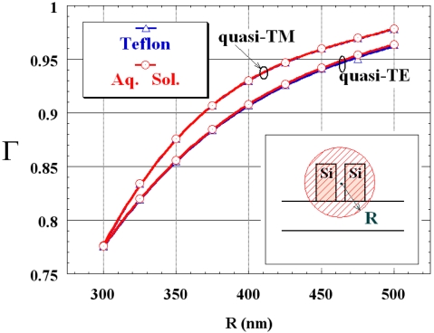
To calculate the distance d between the waveguides in order to achieve a negligible difference between self-coupling coefficients in Eq. (10), the confinement factor Γ in a circle having a radius R and centred at the gap region centre has been evaluated for the single slot waveguide (see inset in Figure 3). Dependence of Γ on R is sketched in Figure 3 for quasi-TE and quasi-TM modes, when the cover medium is either Teflon or an aqueous solution. For R values in the range 300 nm < R < 500 nm, Γ is practically independent from cover refractive index, being larger than 90 % for R ≥ 400 nm, for both polarizations.
Figure 3.
Confinement factor in a circular region versus R (cover medium: Teflon or aqueous solution).
For a distance d ≥ 800 nm between the coupled waveguides, both integrals in Eq. (11) are practically negligible because E1 squared module in W2 region and E2 squared module in W1 region are very close to zero. Then, for d ≥ 800 nm the second additive term in Eq. (10) is negligible, and δ can be estimated by calculating neff,1 and neff,2 through the 2D FEM applied to the two isolated slot waveguides. According with CMT, βc in Eq. (8) can be calculated as [59]:
| (12) |
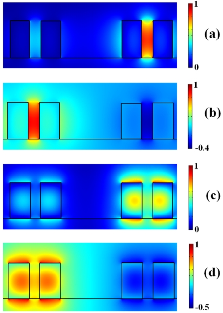
where neff,S and neff,A are the effective indices of the symmetric (S) and antisymmetric (A) supermodes supported by the directional coupler (supermodes profiles are in Figure 4). Supermodes effective indices neff,S and neff,A have been again calculated by 2D full-vectorial FEM applied to the coupler cross-section. Finally, κ2 has been calculated as:
| (13) |
Figure 4.
Main electric field component distribution related to supermodes supported by the asymmetrical directional coupler (d = 1 μm). (a) Quasi-TE symmetric supermode. (b) Quasi-TE antisymmetric supermode. (c) Quasi-TM symmetric supermode. (d) Quasi-TM antisymmetric supermode.
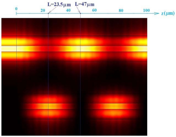
FEM is widely adopted in calculation of mode effective indices because it assures a very high accuracy even for nanometer-scale high index contrast guiding structures. To validate the proposed modelling technique, the asymmetrical directional coupler behaviour has been 3D simulated by EME method [55] in the more sensitive case of quasi-TE polarization. Geometrical parameters reported in Table 1 have been assumed for slot waveguides constituting the coupler with d = 1 μm. In this simulation, cover refractive index is equal to 1.333 for sensing waveguide (W2 in Figure 2), and 1.31 for the other one (W1 in Figure 2). Simulation of optical propagation within the coupler performed by 3D EME method is shown in Figure 5.
Figure 5.
Quasi-TE mode optical propagation in the designed asymmetrical directional coupler (d = 1 μm). Optical field intensity plot obtained by EME method.
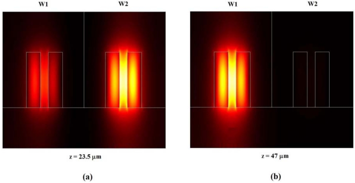
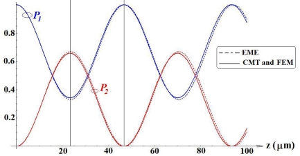
At the section z = 23.5 μm we observe the maximum power transfer from W1 to W2 [see Figure 6(a)], whereas at z = 47 μm the whole optical power is practically confined in W1. The optical intensity distribution in the coupler cross-section for z = 47 μm is shown in Figure 6(b). For z = 23.5 μm, normalized optical powers confined in W1 and W2 have been estimated as 0.3302 and 0.6698, respectively. For z = 47 μm, normalized powers confined in W1 and W2 are equal to 0.9724 and 0.0276, respectively. Normalized optical powers confined in W1 (P1) and W2 (P2) have been also calculated versus propagation direction z by Eqs. (6)–(7) (see Figure 7). The agreement between simulation results obtained by EME method and our modelling procedure is very good, as in Figure 7. From our calculations, coupling length between W1 and W2 is accurately predicted to be z = 23.33 μm.
Figure 6.
Optical intensity (quasi-TE mode by EME method) distribution in the cross-section of asymmetrical directional coupler (d = 1 μm) at: (a) z = 23.5 μm; (b) z = 47 μm.
Figure 7.
Normalized optical power confined in the two coupled waveguides (with d = 1 μm) versus propagation length for quasi-TE mode (Solid curves: modelling technique of this paper based on CMT and FEM; Dashed curves: results by 3D EME method).
4. Sensor optimization and performance
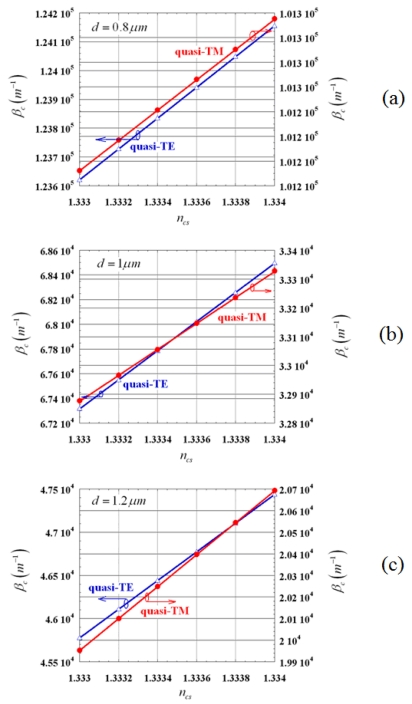
For a given directional coupler length L, the normalized optical power coming out from both waveguides depends on the sensing waveguide (W2) cover index ncs (1.333 ≤ ncs ≤ 1.334) and distance d between the guiding structures. For d = 0.8 μm, 1 μm, 1.2 μm, βc dependence on ncs is sketched in Figure 8 for quasi-TE and quasi-TM modes.
Figure 8.
Dependence of βc on ncs: a) d = 0.8 μm; b) d = 1 μm; c) d = 1.2 μm.
In all considered cases, βc increases with increasing ncs. The ratio between βc values related to quasi-TE and quasi-TM modes is around 1.2 for d = 0.8 μm, 2 for d = 1 μm and, 2.2 for d = 1.2 μm. This implies that P1 varies more rapidly for quasi-TE than for quasi-TM as L changes (see Eq. (6)). βc dependence on ncs is highly linear, so we can get the following formula:
| (14) |
where q0 and q1 are fitting parameters depending on d and mode polarization, as summarized in Table 2.
Table 2.
Fitting parameters q0 and q1 for d = 0.8 μm, 1 μm, 1.2 μm.
| d = 0.8 μm | d = 1 μm | d = 1.2 μm | ||||
|---|---|---|---|---|---|---|
| quasi-TE | quasi-TM | quasi-TE | quasi-TM | quasi-TE | quasi-TM | |
| q0(μm-1) | -0.5894 | -0.0625 | -1.5080 | -0.5688 | -2.1670 | -0.9662 |
| q1(μm-1) | 0.5349 | 0.1228 | 1.1820 | 0.4514 | 1.6601 | 0.7398 |
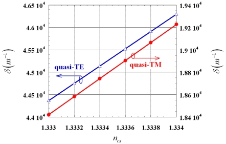
Thus, it is clear that δ does not depend on d (being the second additive term in Eq. (10) negligible under previously discussed conditions), but it is only a function of slot waveguide geometrical parameters and ncs. For quasi-TE and quasi-TM modes, δ dependence on ncs is given in Figure 9.
Figure 9.
δ as a function of ncs for quasi-TE and quasi-TM modes.
For both polarizations, δ increases with increasing ncs, but the phase mismatch between the modes propagating in the coupler waveguides is significantly larger for quasi-TE than for quasi-TM polarization. Because of the linearity of δ dependence on ncs, we can write:
| (15) |
where p0 and p1 are fitting parameters. It results p0 = -2.53 μm-1 and p1 = 1.932 μm-1 for quasi-TE and p0 = -1.056 μm-1 and p1 = 0.806 μm-1 for quasi-TM mode, respectively.
Combining Eq. (6) with Eq. (14) and (15), a new expression of normalized power coming out W1 can be obtained:
| (16) |
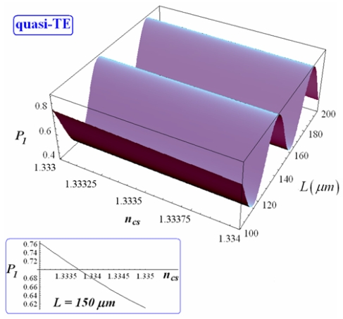
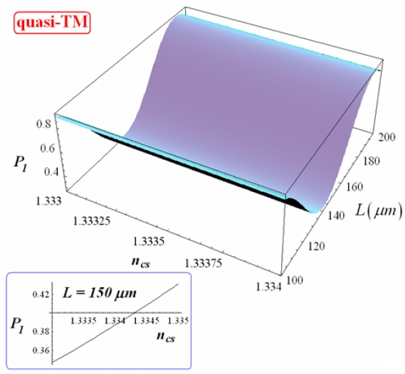
Dependence of P1 on L and ncs is shown in Fig. 10 and 11 for quasi-TE and quasi-TM polarization, respectively (with d = 1 μm and Ψ2 = 0.9).
Figure 10.
Normalized optical power exiting from W1 and its dependence on L and ncs (quasi-TE, d = 1 μm). In the inset the dependence of P1 on ncs is shown assuming L = 150 μm.
Figure 11.
Normalized optical power exiting from W1 and its dependence on L and ncs (quasi-TM, d = 1 μm). In the inset the dependence of P1 on ncs is shown, with L = 150 μm.
As previously mentioned, P1 oscillates as L varies. Oscillation rate is larger for quasi-TE mode than for quasi-TM one. As derived by Eq. (16), since it results (q0 + q1ncs) > (p0 + p1ncs) for each value of d and both polarizations (see Figures 8 and 9), the maximization of P1 requires:
| (17) |
where m is an integer number.
Normalized power coming out W1 has a linear dependence on ncs for each coupler length and both polarizations (see insets in Figures 10 and 11). The sensitivity of normalized power coming out of W1 to ncs change can be defined as:
| (18) |
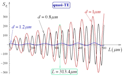
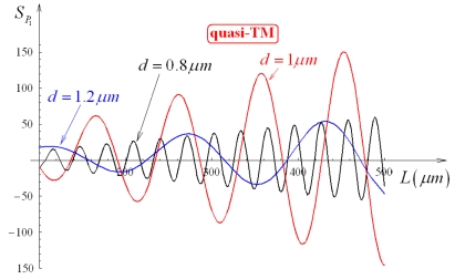
where is the ncs reference value in which the derivative is calculated (we have assumed ). This sensitivity is shown in Figures 12 and 13 as a function of L, for d = 0.8 μm, 1 μm, 1.2 μm and quasi-TE and quasi-TM polarizations, respectively. By comparing Figure 12 with 13, we can observe SP1 as significantly larger for quasi-TE than for quasi-TM mode and oscillating as L increases (oscillations are slower for quasi-TM than for quasi-TE). Values of relative maxima of SP1 progressively increase by increasing L, thus an arbitrary SP1 value could be obtained by simply increasing L. However, an appropriate trade-off between coupler sensitivity and length has to be usually achieved.
Figure 12.
SP1 dependence on L, for d equal to 0.8 μm, 1 μm, 1.2 μm (quasi-TE, Ψ2 = 0.9).
Figure 13.
SP1 dependence on L, for d equal to 0.8 μm, 1 μm, 1.2 μm (quasi-TM, Ψ2 = 0.9).
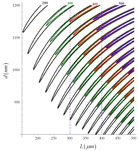
For d = 1 μm, larger sensitivity values can be obtained for either quasi-TE or quasi-TM modes. For example, assuming d = 1 μm and L = 313.4 μm, a sensitivity SP1 = 215.29 is obtained for quasi-TE mode. SP1 dependence on d and L has been investigated for quasi-TE mode by calculating SP1 level curves, as sketched in Figure 14.
Figure 14.
Level curves of SP1 as a function of L and d (quasi-TE mode, Ψ2 = 0.9).
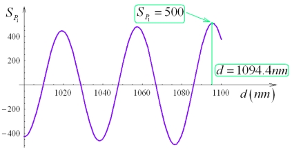
Increasing both geometrical parameters (i.e. sensor total area), an improvement of sensitivity can be observed. Assuming for SP1 a target value of 500, we observe that this sensitivity value cannot be obtained for L = 300 μm, while becoming achievable for L = 400 μm. SP1 dependence on d has been investigated for L = 400 μm and quasi-TE polarization (see Figure 15), observing again an oscillatory behaviour. Minimum d value to achieve SP1 = 500 is equal to 1,094.4 nm. Geometrical parameters of the optimized sensor are summarized in Table 3.
Figure 15.
SP1 as a function of d for L = 400 μm (quasi-TE mode, Ψ2 = 0.9).
Table 3.
Geometrical and performance parameters of the optimized directional coupler for optical chemical sensing (slot waveguides parameters are in Table 1).
| Parameter | Value |
|---|---|
| Coupler length (L) | 400 μm |
| Distance between slot waveguides (d) | 1,094.4 nm |
| Device area | 1,200 μm2 |
| SP1 (quasi-TE mode) | 500 |
| S(P1–P2) (quasi-TE mode) | 1,000 |
| Minimum detectable refractive index change | 10-5 |
| Minimum detectable glucose concentration | 0.1 g/L |
In a directional coupler, the sum of normalized optical powers coming out from W1 and W2 is a constant value, Ψ2. Thus, the difference between P1 and P2 can be written as:
| (19) |
Therefore, the power difference sensitivity to the sensing waveguide cover index change is given by:
| (20) |
Using the coupler sizes in Table 3, a value of S(P1–P2) = 1,000 can be obtained.
This means that, if a (P1-P2) shift equal to 1% is detectable by the photo-detection apparatus, a change of ncs value of the order of 10-5 could be detected by a device having a length of 400 μm and a total area of 1,200 μm2. This value of minimum detectable refractive index is well five times lower than that reported for an integrated optical chemical sensor based on a conventional 10 mm long directional coupler [2], and about two times lower than that for a ring resonator-based optical biosensor, having a total area of 11,300 μm2 [9]. The integrated optical chemical sensor reported in [3] is very sensible, having a minimum detectable change of mode effective index as low as 10-8. However, this result is obtained by integrating a phase modulator within the sensor, i.e. at the expenses of device complexity and very large sensor dimensions (device area = 8×107 μm2).
If the sensor designed in this paper is used to sense glucose concentration, its sensitivity should be around 0.1 g/L. Moreover, the theoretical minimum detectable refractive index in our architecture is more than one order of magnitude lower than that experimentally obtained value by the sensor reported in [51], having an area of 19,600 μm2 and adopting a Si3N4/SiO2 slot waveguide.
5. Conclusions
In this paper, we have proposed, modelled and optimized a directional coupler-based integrated optical chemical sensor. The coupler is formed by two nanometer-scale SOI slot waveguides. Monitoring the difference between optical power coming out from the two waveguides, it is possible to estimate with high accuracy the concentration of an analyte in the aqueous solution used as cover medium of one of the two waveguides forming the coupler. Sensor modelling is carried out by using the coupled mode theory formulation, while coupling coefficients between propagating modes and their phase mismatch are estimated by 2D full-vectorial finite element method. This modelling technique has been validated by comparing its results with those provided by the highly accurate 3D EME method.
An effective optimization procedure has been developed to obtain a very good trade-off between sensor dimensions and sensitivity. A minimum detectable refractive index change of the order of 10-5 can be obtained by a device having a very reduced occupation area, equal to 1,200 μm2. Because the photonic sensor is based on the use of an asymmetric directional coupler, read-out apparatus is expected to be very simple, i.e. to measure an analyte concentration shift it should be necessary to sense only an optical power change. If the sensor is used to estimate the glucose concentration in an aqueous solution, a resolution around 0.1 g/L can be theoretically predicted.
References
- 1.Passaro V.M. N., Dell'Olio F., Casamassima B., De Leonardis F. Guided-Wave Optical Biosensors. Sensors. 2007;7:508–536. [Google Scholar]
- 2.Luff B.J., Harris R. D., Wilkinson J. S., Wilson R., Schiffrin D. J. Integrated-optical directional coupler biosensor. Opt. Lett. 1996;21:618–620. doi: 10.1364/ol.21.000618. [DOI] [PubMed] [Google Scholar]
- 3.Heideman R.G., Lambeck P. V. Remote opto-chemical sensing with extreme sensitivity: design, fabrication and performance of a pigtailed integrated optical phase-modulated Mach-Zehnder interferometer system. Sens. Actuat. B. 1999;61:100–127. [Google Scholar]
- 4.Prieto F., Sepulveda B., Calle A., Llobera A., Domynguez C., Abad A., Montoya A., Lechuga L.M. An integrated optical interferometric nanodevice based on silicon technology for biosensor applications. Nanotechnology. 2003;14:907–912. [Google Scholar]
- 5.Brosinger F., Freimuth H., Lacher M., Ehrfeld W., Gedig E., Katerkamp A., Spenser F., Camman K. A label-free affinity sensor with compensation of unspecific protein interaction by a highly sensitive integrated optical Mach-Zehnder interferometer on silicon. Sens. Actuat. B. 1997;44:350–355. [Google Scholar]
- 6.Hopman W.C. L., Pottier P., Yudistira D., van Lith J., Lambeck P. V., De La Rue R. M., Driessen A. Quasi-one-dimensional photonic crystal as a compact building-block for refractometric optical sensors. IEEE J. Sel. Top. Quant. Electron. 2005;11:11–16. [Google Scholar]
- 7.Passaro V.M. N., Loiacono R., D'Amico G., De Leonardis F. Design of Bragg Grating Sensors Based on Submicrometer Optical Rib Waveguides in SOI. IEEE Sensors J. 2008;11:1603–1611. [Google Scholar]
- 8.Chao C.Y., Fung W., Guo L. J. Polymer microring resonators for biochemical sensing applications. IEEE J. Sel. Top. Quant. Electron. 2006;12:134–142. [Google Scholar]
- 9.Yalçyn A., Popat K.C., Aldridge J. C., Desai T.A., Hryniewicz J., Chbouki N., Little B. E., King O., Van V., Chu S., Gill D., Anthes-Washburn M., Unlu M. S., Goldberg B. B. Optical sensing of biomolecules using microring resonators. IEEE J. Sel. Top. Quant. Electron. 2006;12:148–155. [Google Scholar]
- 10.Passaro V.M. N., Dell'Olio F., De Leonardis F. Ammonia Optical Sensing by Microring Resonators. Sensors. 2007;7:2741–2749. doi: 10.3390/s7112741. [DOI] [PMC free article] [PubMed] [Google Scholar]
- 11.Ciminelli C., Armenise M.N. Modeling and design of a 2D photonic crystal microcavity on polymer material for sensing applications. Proc. SPIE. 2007;6619:661933. [Google Scholar]
- 12.Passaro V. M. N. Silicon Photonics. Research Signpost; Kerala, India: 2006. [Google Scholar]
- 13.Timotijevic B.D., Gardes F. Y., Headley W. R., Reed G. T., Paniccia M., Cohen O., Hak D., Masanovic G. Z. Multi stage racetrack resonator filters in silicon-on-insulator. J. Opt A, Pure Appl. Opt. 2006;8:S473–S476. [Google Scholar]
- 14.Canning J., Sceats M.G., Fleming S. Grating structures with phase mask period in silica-on-silicon planar waveguides. Optics Comm. 1999;171:213–217. [Google Scholar]
- 15.Barrios C.A., Almeida V. R., Panepucci R. R., Schmidt B. S., Lipson M. Compact Silicon Tunable Fabry-Perot Resonator with Low Power Consumption. IEEE Photon. Tech. Lett. 2004;16:506–508. [Google Scholar]
- 16.Almeida V.R., Xu Q., Barrios C. A., Lipson M. Guiding and confining light in void nanostructure. Opt. Lett. 2004;29:1209–1211. doi: 10.1364/ol.29.001209. [DOI] [PubMed] [Google Scholar]
- 17.Jordana E., Fedeli J. M., El Melhaoui L., Lyan P., Colonna J.P., Daldosso N., Pavesi L., Pellegrino P., Garrido B., Vilà A., Lebour Y. Eur. Conf. Integrated Optics Proc. WB4, Copenhagen; Denmark: 2007. Apr 25-27, Deep-UV Lithography Fabrication of Slot Waveguides and Sandwiched Waveguides for Nonlinear Applications. [Google Scholar]
- 18.Xu Q., Almeida V.R., Panepucci R. R., Lipson M. Experimental demonstration of guiding and confining light in nanometer-size low-refractive-index material. Opt. Lett. 2004;29:1626–1628. doi: 10.1364/ol.29.001626. [DOI] [PubMed] [Google Scholar]
- 19.Baehr-Jones T., Hochberg M., Walker C., Scherera A. High-Q optical resonators in silicon-on-insulator-based slot waveguides. Appl. Phys. Lett. 2005;86:081101. [Google Scholar]
- 20.Schrauwen J., Van Lysebettens J., Claes T., De Vos K., Bienstman P., Van Thourhout D., Baets R. Focused-ion-beam fabrication of slots in silicon waveguides and ring resonators. IEEE Photon. Technol. Lett. 2009;21 in publication. [Google Scholar]
- 21.Barrios C. A., Xu Q., Shakya J., Manolatou C., Lipson M. OSA Conf. on Lasers and Electro-Optics/Quantum Electronics and Laser Science and Photonic Applications Systems Technologies. Technical Digest; 2006. Compact silicon slot-waveguide disk resonator. paper CTuCC3. [Google Scholar]
- 22.Barrios C.A. High-performance all-optical silicon micro-switch. Electron. Lett. 2004;40:862–863. [Google Scholar]
- 23.Baehr-Jones T., Hochberg M., Wang G., Lawson R., Liao Y., Sullivan P.A., Dalton L., Jen A. K.-Y., Scherer A. Optical modulation and detection in slotted silicon waveguides. Opt. Express. 2005;13:5216–5226. doi: 10.1364/opex.13.005216. [DOI] [PubMed] [Google Scholar]
- 24.Hochberg M., Baehr-Jones T., Wang G., Huang J., Sullivan P., Dalton L., Scherer A. Towards a millivolt optical modulator with nano-slot waveguides. Opt. Express. 2007;15:8401–8410. doi: 10.1364/oe.15.008401. [DOI] [PubMed] [Google Scholar]
- 25.Baehr-Jones T., Penkov B., Huang J., Sullivan P., Davies J., Takayesu J., Luo J., Kim T.-D., Dalton L., Jen A., Hochberg M., Scherer A. Nonlinear polymer-clad silicon slot waveguide modulator with a half wave voltage of 0.25 V. Appl. Phys. Lett. 2008;92:163303. [Google Scholar]
- 26.Barrios C.A. Ultrasensitive Nanomechanical Photonic Sensor Based on Horizontal Slot-Waveguide Resonator. IEEE Photon. Technol. Lett. 2006;18:2419–2421. [Google Scholar]
- 27.Barrios C.A., Lipson M. Electrically driven silicon resonant light emitting device based on slot waveguide. Opt. Express. 2005;13:10092–10101. doi: 10.1364/opex.13.010092. [DOI] [PubMed] [Google Scholar]
- 28.Fujisawa T., Koshiba M. Polarization-independent optical directional coupler based on slot waveguides. Opt. Lett. 2006;31:56–58. doi: 10.1364/ol.31.000056. [DOI] [PubMed] [Google Scholar]
- 29.Magno F., Passaro V. M. N., Dell'Olio F., De Leonardis F. Investigation of Silicon Slot-based Directional Couplers. Eur. Conf. Integrated Optics Proc. 2007 Apr 25-27 ThG24, Copenhagen. [Google Scholar]
- 30.Fujisawa T., Koshiba M. All-optical logic gates based on nonlinear slot-waveguide couplers. J. Opt. Soc. Am. B. 2006;23:684–691. [Google Scholar]
- 31.Fujisawa T., Koshiba M. Theoretical Investigation of Ultrasmall Polarization-Insensitive 1 × 2 Multimode Interference Waveguides Based on Sandwiched Structures. IEEE Photon. Technol. Lett. 2006;18:1246–1248. [Google Scholar]
- 32.Xiao J., Liu X., Sun X. Design of an ultra-compact MMI wavelength demultiplexer in slot waveguide structures. Opt. Express. 2007;15:8300–8308. doi: 10.1364/oe.15.008300. [DOI] [PubMed] [Google Scholar]
- 33.Feng N.-N., Michel J., Kimerling L. C. Low-loss compact-size slotted waveguide polarization rotator and transformer. Opt. Lett. 2007;32:2131–2133. doi: 10.1364/ol.32.002131. [DOI] [PubMed] [Google Scholar]
- 34.Riboli F., Bettotti P., Pavesi L. Band gap characterization and slow light effect in one dimentional photonic crystals based on silicon slot-waveguides. Opt. Express. 2007;15:11769–11775. doi: 10.1364/oe.15.011769. [DOI] [PubMed] [Google Scholar]
- 35.Mu J., Zhang H., Huang W.-P. A Theoretical Investigation of Slot Waveguide Bragg Gratings. IEEE J. Quantum Electron. 2008;44:622–627. [Google Scholar]
- 36.Yang A.H. J., Moore S. D., Schmidt B. S., Klug M., Lipson M., Erickson D. Optical manipulation of nanoparticles and biomolecules in sub-wavelength slot waveguides. Nature. 2009;457:71–75. doi: 10.1038/nature07593. [DOI] [PubMed] [Google Scholar]
- 37.Sanchis P., Blasco J., Martínez A., Martí J. Design of Silicon-Based Slot Waveguide Configurations for Optimum Nonlinear Performance. J. Lightwave Technol. 2007;25:1298–1305. [Google Scholar]
- 38.Fujisawa T., Koshiba M. Guided Modes of Nonlinear Slot Waveguides. IEEE Photon. Technol. Lett. 2006;18:1530–1532. [Google Scholar]
- 39.Passaro V. M. N., Lagioia M., De Leonardis F. Design of nonlinear SOI slot waveguides. Proc. 14th Eur. Conf. Int. Optics (ECIO 2008) :225–228. ThP13. [Google Scholar]
- 40.Feng N.-N., Sun R., Kimerling L. C., Michel J. Lossless strip-to-slot waveguide transformer. Opt. Lett. 2007;32:1250–1252. doi: 10.1364/ol.32.001250. [DOI] [PubMed] [Google Scholar]
- 41.Galan J.V., Sanchis P., Blasco J., Marti J. Study of High Efficiency Grating Couplers for Silicon-Based Horizontal Slot Waveguides. IEEE Photon. Technol. Lett. 2008;20:985–987. [Google Scholar]
- 42.Barrios C.A., Sánchez B., Gylfason K. B., Griol A., Sohlström H., Holgado M., Casquel R. Demonstration of slot-waveguide structures on silicon nitride/silicon oxide platform. Opt. Express. 2007;15:6846–6856. doi: 10.1364/oe.15.006846. [DOI] [PubMed] [Google Scholar]
- 43.Müllner P., Hainberger R. Structural Optimization of Silicon-On-Insulator Slot Waveguides. IEEE Photon. Technol. Lett. 2006;18:2557–2559. [Google Scholar]
- 44.Preston K., Lipson M. Slot waveguides with polycrystalline silicon for electrical injection. Opt. Express. 2009;17:1527–1534. doi: 10.1364/oe.17.001527. [DOI] [PubMed] [Google Scholar]
- 45.Galli M., Gerace D., Politi A., Liscidini M., Patrini M., Andreani L.C., Canino A., Miritello M., Lo Savio R., Irrera A., Priolo F. Direct evidence of light confinement and emission enhancement in active silicon-on-insulator slot waveguides. Appl. Phys. Lett. 2006;89:241114. [Google Scholar]
- 46.Feng N.-N., Michel J., Kimerling L. C. Optical Field Concentration in Low-Index Waveguides. IEEE J. Quant. Electron. 2006;42:885–890. [Google Scholar]
- 47.Chen X., Jiang W., Chen J., Gu L., Chen R.T. 20 dB-enhanced coupling to slot photonic crystal waveguide using multimode interference coupler. Appl. Phys. Lett. 2007;91:091111. [Google Scholar]
- 48.Wülbern J.H., Petrov A., Eich M. Electro-optical modulator in a polymer infiltrated silicon slotted photonic crystal waveguide heterostructure resonator. Opt. Express. 2009;17:304–313. doi: 10.1364/oe.17.000304. [DOI] [PubMed] [Google Scholar]
- 49.Veronis G., Fan S. Modes of Subwavelength Plasmonic Slot Waveguides. J. Lightwave Technol. 2007;25:2511–2521. [Google Scholar]
- 50.Dell'Olio F., Passaro V.M. N. Optical sensing by optimized silicon slot waveguides. Opt. Express. 2007;15:4977–4993. doi: 10.1364/oe.15.004977. [DOI] [PubMed] [Google Scholar]
- 51.Barrios C.A., Gylfason K. B., Sánchez B., Griol A., Sohlström H., Holgado M., Casquel R. Slot-waveguide biochemical sensor. Opt. Lett. 2007;32:3080–3082. doi: 10.1364/ol.32.003080. [DOI] [PubMed] [Google Scholar]
- 52.Barrios C.A., Bañuls M. J., González-Pedro V., Gylfason K. B., Sánchez B., Griol A., Maquieira A., Sohlström H., Holgado M., Casquel R. Label-free optical biosensing with slot-waveguides. Opt. Lett. 2008;33:708–710. doi: 10.1364/ol.33.000708. [DOI] [PubMed] [Google Scholar]
- 53.Robinson J.T., Chen L., Lipson M. On-Chip Gas Detection in Silicon Optical Microcavities. Opt. Express. 2008;16:4296–4301. doi: 10.1364/oe.16.004296. [DOI] [PubMed] [Google Scholar]
- 54.Comsol Multiphysics by COMSOL © single license 2005 ver. 3.2. [Google Scholar]
- 55.FIMMPROP by Photon Design © single license. 2007 ver. 4.6. [Google Scholar]
- 56.Yeh Y. L., Wang C. C., Jang M. J., Chen C. H., Tzeng S. M., Lin Y. P., Chen K. S. Real-time measurement of glucose concentration using position sensing detector. Proc. 3rd IEEE Int. Conf. Nano/Micro Engineered Molec. Syst. 2008:561–565. [Google Scholar]
- 57.Datta A., Eom I.-Y., Dhar A., Kuban P., Manor R., Ahmad I., Gangopadhyay S., Dallas T., Holtz M., Temkin H., Dasgupta P. K. Microfabrication and Characterization of Teflon AF-Coated Liquid Core Waveguide Channels in Silicon. IEEE Sensors J. 2003;3:788–795. [Google Scholar]
- 58.Parriaux O., Lambeck P.V., Hoekstra H. J.W. M., Veldhuis G. J., Pandraud G. Evanescent wave sensor of sensitivity larger than a free space wave. Opt. Quant. Electron. 2000;32:909–921. [Google Scholar]
- 59.Liu J. M. Photonic Devices. Cambridge University Press; Cambridge: 2005. [Google Scholar]


