Abstract
Recent studies show that reduction in cross-sectional area can be used to improve the concentration factor in microscale bioseparations. Due to simplicity in fabrication process, a step reduction in cross-sectional area is generally implemented in microchip to increase the concentration factor. But the sudden change in cross-sectional area can introduce significant band dispersion and distortion. This paper reports a new fabrication technique to form a gradual reduction in cross-sectional area in polymethylmethacrylate (PMMA) microchannel for both anionic and cationic isotachophoresis (ITP). The fabrication technique is based on hot embossing and surface modification assisted bonding method. Both one-dimensional and two-dimensional gradual reduction in cross-sectional area microchannels were formed on PMMA with high fidelity using proposed techniques. ITP experiments were conducted to separate and preconcentrate fluorescent proteins in these microchips. Thousand fold and ten thousand fold increase in concentrations were obtained when 10 × and 100 × gradual reduction in cross-sectional area microchannels were used for ITP.
INTRODUCTION
Polymethylmethacrylate (PMMA) is a widely used material to form microfluidic device for biomedical and biotechnology applications because it is cheap, disposable, and biocompatible, and it possesses excellent optical properties such as low autofluorescence1 and high transparency.2 PMMA microfluidic device is also less prone to mechanical failure due to very high bonding strength. For instance, a PMMA microchip can withstand as high as 300 psi pressure, while a typical polydimethylsiloxane (PDMS) microchannel delaminates at pressure higher than 50 psi.3
Several fabrication methods have been reported to produce PMMA and other thermoplastic microfluidic devices.4 Of these methods, embossing is relatively simple, low cost, and easy to implement. Embossing can be performed using thermal effect (hot embossing)5 or with the aid of a solvent (e.g., acetonitrile, chloroform, isopropanol).6 Also depending on the characteristic feature of the end product, the embossing technique can be carried out with metallic masters or microfabricated molds.
In hot embossing with metal master,7 a master mold is imprinted on a plain PMMA substrate at glass transition temperature of PMMA. Generally direct structuring of this metal master is performed using mechanical machining or laser ablation. Though these techniques ensure great precision and are readily manufacturable, master produced via these techniques do not offer smooth surface finishes and high aspect ratios, and usually not suitable for microfabrication process.8
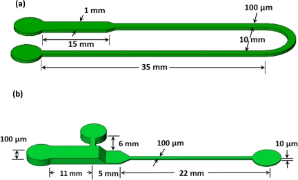
Embossing with polymer micro mold is very popular technique in microfabrication where a SU-8 pattern is generally formed with standard photolithography; this photolithography provides high aspect ratio, smaller feature sizes and smoother wall finish. In solvent based embossing of microchannel, a solvent (e.g., chloroform, acetonitrile) is used to soften the PMMA and emboss the SU-8 master into PMMA using moderate pressure. Since a solvent is used for the softening process, it is very difficult to optimize the process parameters to maintain precise dimensions of microchannel in solvent based imprinting method. On the other hand, in hot embossing with microfabricated SU-8 master, the mold is imprinted on a PMMA substrate with controlled temperature and pressure. This technique is low cost and simple, and it is easy to control the process parameters to replicate the master on PMMA surface precisely. Although hot embossing is quite popular for fabricating simple microchannel, this technique is not very effective if the mold is not planar. In other words, the standard hot embossing technique does not work for complex microchannels such as horseshoe or dog-leg channel (Figure 1) especially when there is a change in cross-sectional area due to variable height in addition to the change in the width direction.
Figure 1.
Schematic of PMMA microchips used for ITP experiments. (a) 1D gradual reduction U shaped chip. This chip has a 10× reduction in cross-sectional area. (b) 2D gradual reduction (with a width and a depth change along the channel) cascade chip. The depth change begins right after the T-junction. The T-junction is used to control the sample loading in the microchip platform. This microchip includes a 100× reduction in cross-sectional area from the large cross-sectional area region (1 mm wide × 100 μm deep) to the small cross-sectional area region (100 μm wide × 10 μm deep).
In recent years, there are strong demands for variable cross-sectional area microchannel for preconcentration of biomolecules9 and ions.10 The reduction in cross-sectional area can improve the concentration factor significantly in peak mode isotachophoresis as the concentration factor is proportional to the ratio of initial to final cross-sectional area.11 Usually reduction in cross-sectional area is achieved by changing the channel width in a planar microfabrication technique. A two-dimensional change in the cross-sectional area is more effective than just decreasing the channel width for preconcentration of ions or proteins. However, it remains a major challenge to avoid the delamination of the master from substrate during imprinting/embossing, if the mold has variable cross-section.
In microfabrication, there are a number of choices for substrates (e.g., silicon wafer, glass, PMMA) to form SU-8 mold. Silicon substrates provide very good adhesion12 with SU-8 mold for embossing, but problems arise at the interface of SU-8 and underlying silicon substrate at elevated temperature.13 Moreover, silicon wafer is very expensive compared to other silicon based substrates. Glass can be used as a low cost alternative to silicon, but glass is also prone to delamination during imprinting due to poor adhesion between SU-8 and glass substrate. Moreover, the low refractive index of glass (n = 1.47) causes partial UV transmission that can cause unwanted internal reflections which is a major reason for low quality SU-8 master on glass.14 In recent years, Chiang et al. has done experiments on various plastic substrates for SU-8 photolithography and found that PMMA is suitable for this purpose.15 However, PMMA requires special coating to remove unwanted refraction due to low refractive index (n = 1.49) (Ref. 14) and PMMA substrate is especially not suitable if the microchannel is formed on PMMA. So it is necessary to explore an alternative substrate for fabrication of complex microchip on PMMA. In this study, we chose polyetherimide (PEI), a new substrate, for this fabrication process because of its high refractive index (n = 1.68) and other properties compatible with PMMA and SU-8. For comparison, microscale molds were also fabricated on glass substrate to form complex microchannel.
The rest of the paper is organized as follows. First, we have presented a methodology for 2D gradual reduction (changes in size both in width and depth directions) cascade chip fabrication, and qualitatively investigated the performance of different substrates. Next, we have compared the adhesion strength of SU-8 with these substrates and investigated the thermal properties of materials involved in microchip fabrication to identify the reasons for performance variation of different substrates. Finally, using PEI as substrate, we fabricated PMMA microchips with one-dimensional (Figure 1a) and two-dimensional (Figure 1b) gradual change in cross-sectional area, and used them to perform anionic and cationic isotachophoresis (ITP).
MICROCHIP FABRICATION
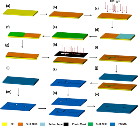
Microfabrication techniques are developed for two-dimensional (2D) gradual change in cross-sectional area channel as shown in Figure 1b. Figure 2 shows the schematic of the fabrication processes. The fabrication processes consist of multilayer photolithography for mold, hot embossing for imprinting of channel structure, and surface modification assisted bonding for contained and sealed housing.
Figure 2.
PEI substrate based PMMA microchip fabrication process. (a) Cleaning PEI slide, (b) spinning of SU-8 2010, (c) UV exposing of SU-8, (d) covering with Teflon Tape, (e) spinning of SU-8 2035, (f) removing of Teflon tape, (g) spinning of SU-8 2010, (h) positive patterning, (i) developing the pattern, (j) hot embossing on PMMA, (k) imprinted PMMA, (l-m) cleaning and drilling holes on a PMMA substrate, (n) aligning of PMMA substrates after surface treatment, and (o) bonding of two PMMA substrates with specified pressure and temperature.
The mold fabrication processes were carried out on two different substrates: glass and PEI. The basic steps for mold fabrication are identical for these substrates, but process parameters were optimized to get better results. In this section, mold fabrication techniques are only described for PEI substrate (Figures 2a, 2b, 2c, 2d, 2e, 2f, 2g, 2h, 2i), and relevant parameters for glass substrate are shown in Table TABLE I..
TABLE I.
Fabrication protocol used to form cascade SU-8 master on different substrates.
| PEI substrate | Glass substrate | |
|---|---|---|
| Spinning of SU-8 2010 | 3000 rpm (30 s) | 3000 rpm (30 s) |
| Prebake | 105 °C (8 min) | 100 °C (6 min) |
| UV expose | 150 mJ/cm2 | 150 mJ/cm2 |
| Post bake | 110 °C (10 min) | 105 °C (10 min) |
| Covering with Teflon tape | Half of the slide | Half of the slide |
| Spinning of SU-8 2035 | 1400 rpm (30 s) | 1400 rpm (30 s) |
| Spreading of SU-8 2035 | 2 min | 2 min |
| Prebake | 105 °C (15 min) | 100 °C (12 min) |
| Spinning of SU-8 2010 | 3000 rpm (30 s) | 3000 rpm (30 s) |
| Prebake | 75 °C (5 min) and 105 °C (15 min) | 70 °C (5 min) and 100 °C (12 min) |
| UV expose | 450 mJ/cm2 | 450 mJ/cm2 |
| Post bake | 110 °C (15 min) | 105 °C (15 min) |
| Develop | 25 min | 15 min |
| Hard bake | 200 °C (15 min) | 200 °C (15 min) |
In the 2D gradual change cross-sectional area microchannel, there are three different depth sections (100 μm, 10 μm, and 100 to 10 μm) as well as change in channel width. Thus to form a three dimensional mold, we used multilayer spinning on a custom-cut PEI substrate (7.0 cm × 5.0 cm, McMaster-Carr, CA). At the beginning of photolithography, a thin SU-8 layer of ∼10 μm was formed on PEI substrate to increase the adhesion strength of SU-8 pattern and PEI (Fig. 2b). This layer was fabricated by spinning SU-8 2010 (MicroChem Corp., MA, USA) on PEI substrate at 3000 rpm for 30 s. Next photoresist coated PEI substrate was heated on a hot plate (Digital Hot Plate/Stirrer, Series 04644, Cole Parmer, IL, USA) at 105 °C for 8 min. The photoresist was then exposed to near ultraviolet light (365 nm) at 150 mJ/cm2 for 43 s using a mask aligner (Hybralign, Series 500, Optical Associates Inc., CA, USA) (Fig. 2c). Next, the PEI substrate was post-baked on a hot plate at 110 °C for 5 min. The thin layer was then covered partially (based on the microchip design) with Teflon tape (Precision Coating Co. Inc., MA, USA) (Fig. 2d). Then SU-8 2035 (Microchem Crop., MA) was spun on the thin layer at 1400 rpm for 30 s to get a 90 μm thick layer (Fig. 2e). After spin coating, the tape was removed so that the SU-8 can spread over (Fig. 2f) and provide a transitional depth within the specified length. The PEI substrate was then prebaked at 105 °C for 15 min. Next SU-8 2010 was spun coated on the entire PEI substrate at 3000 rpm (Fig. 2g). This yielded another 10 μm thick SU-8 layer. The SU-8 photoresist was then prebaked at 75 °C for 5 min and 105 °C for 15 min and exposed to UV light through direct contact with a patterned mask that contains the desired microchip feature (Fig. 2h). The ultraviolet radiation causes the negative resist to become polymerized, which makes it more difficult to dissolve. Next the PEI substrate was post baked at 110 °C for 15 min, and finally developed with commercially available SU-8 developer (MicroChem Corp., MA, USA) (Fig. 2i). The developer solution removed only the unexposed portions of the photoresist, and the negative resist remained on the PEI slide wherever it was exposed. Thus the SU-8 master of desired channel structure was fabricated on PEI substrate. The length of 100-10 μm transition region was measured with a profilometer (SPN Technology, Inc., CA), and its value varied between 0.67 mm and 0.71 mm (not shown). It has been observed that the length of the transition region depends on the height of SU-8 2035 layer, and viscosities of photoresists have very minor role.
Next SU-8 master was hot embossed into a PMMA substrate using a hot press (Manual Bench Top Laboratory Press, Model 3851, Carver Inc., IN, USA). First, a UV transparent PMMA piece (ACRYLITE® OP-4, Evonik Cyro LLC, NJ, USA) was trimmed to size (7.0 cm × 5.0 cm × 0.4 cm) and cleaned with soapy water, rinsed, and dried under nitrogen. The PMMA substrate was then placed on the PEI slide containing SU-8 master (Fig. 2j). Next the whole assembly was placed in the hot press for 1 min at 120 °C. This heating process mainly softens the surface of the PMMA substrate that is in contact with SU-8 master. Then 350 psi pressure was applied gradually and held it for 1 min. The hot plate was then cooled down just below the glass transition temperature of PMMA using a built-in water cooling mechanism and the PEI slide was removed from the PMMA substrate to get the bottom layer of the microchip (Fig. 2k). Similar embossing techniques are followed for mold formed on glass.
Next this open channel was bonded with a flat surface of another PMMA substrate using surface modification assisted bonding.16 In the bonding process, first a second piece of PMMA was trimmed to size, cleaned and dried (Fig. 2l). Then inlets and outlets reservoirs were drilled in appropriate locations (Fig. 2m). This was followed by surface modification of both PMMA substrates using oxygen plasma and tetraethyl orthosilicate (99% TEOS, Sigma-Aldrich, St Louis, MO, USA). The two substrates were then aligned (Fig. 2n) and brought into contact and pressed together with a hot press for 15 min at 75 °C and 400 psi to form the final microchip (Fig. 2o). Finally, the bonded chip was baked at 70 °C for 3 h to increase the bonding strength. PMMA microchip formed using aforementioned techniques are used to concentrate low abundance proteins using anionic and cationic isotachophoresis.
TEST
Easiness of SU-8 master fabrication
The easiness of SU-8 master fabrication on different substrates was monitored qualitatively especially in the master developing stage (Fig. 2i) of photolithography. For glass substrate, successful developing is very time sensitive and removal of SU-8 layers happens if the developing time is longer than the optimum. In a cascade mold, it requires variable developing times for different sections. For instance, the thicker (∼100 μm) section required more time for developing and it eventually caused the removal of thin (∼10 μm) base layer (as shown in Fig. 2c). On the other hand, if no base layer is used, the low thickness section (small cross-sectional area) of the mold is removed before the thicker section is fully developed. However, the master fabrication process on PEI substrate is not very time sensitive and the success rate is almost 100%. The authors do not completely understand why PEI has better performance than glass substrate. Two plausible hypotheses are (a) UV exposure creates stronger bond between SU-8 and PEI substrate than that of SU-8 and glass and (b) delamination of SU-8 layer from glass substrate during the baking process due to the very large difference in the coefficient of thermal expansion (CTE) between SU-8 (50e-6 K−1) and glass (8.5e-6 K−1).17
Delamination of SU-8 master from substrate during hot embossing
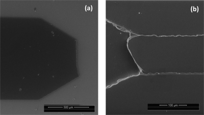
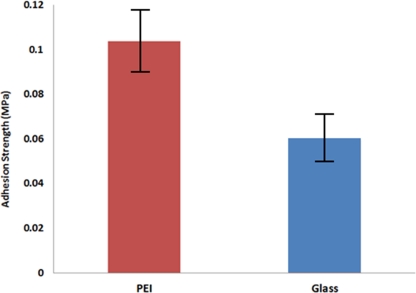
It was observed that a portion of master (SU-8) was always retained within the PMMA during the imprinting process when the master was formed on glass substrate (Fig. 3). However, no such attachment of SU-8 part on the PMMA channel was observed when the pattern was formed on PEI, and we were able to use these patterns for multiple imprintings on PMMA. To investigate the disintegration of molds from different substrates, we ran adhesion strength test of SU-8 with these substrates and studied the thermal properties of materials used in the fabrication process.
Figure 3.
Photographs of (a) delamination of a SU-8 master from a glass substrate after de-embossing and (b) adherence of a portion of SU-8 master on a PMMA after de-embossing.
Adhesion test
The adhesion strength of SU-8 with different substrates was measured quantitatively using Instron (Model TT, Instron, MA, USA) tensile testing machine. The test was performed after fabricating a 10 μm base layer on the substrate as described in Figs. 2a to 2c. However instead of making the layer on whole domain, we used a patterning mask (contains a 10 mm × 10 mm rectangular window) in the UV exposure step (Fig. 2b) and the SU-8 layer was developed and post baked on hot plate to get a rectangular feature.
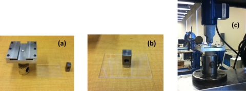
The fabricated SU-8 master was then glued to a custom made rectangular block (Fig. 4) with Permaoxy (Permatex, OH, USA) epoxy. Before applying the epoxy the substrate was fully covered with Teflon tape (Precision Coating Co. Inc., MA, USA) except the SU-8 master region. Thus, it prevents the epoxy to come in direct contact with the substrate. After hardening of epoxy for 5 h at 80 °C in the oven, the Teflon tape was removed from the substrate. The substrate was then mounted on the tensile testing machine with a custom made fixture/holder (Fig. 4). The force required breaking the SU-8—substrate bond was recorded using a 25 lb load cell. A photograph of mounted substrate on a tensile testing facility is shown in Fig. 4. Comparative results of adhesion strength of SU-8 master with different substrates were presented in Fig. 5. The adhesion strength of PEI was found little bit higher than that of glass.
Figure 4.
Experimental setup for adhesion strength test, (a) custom made holder, a typical substrate and custom made rectangular block (left to right). (b) The rectangular block is glued on the SU-8 layer (on substrate). (c) The assembly is slided through the custom made fixture and finally is mounted on the Tensile testing machine.
Figure 5.
Interfacial adhesion strength of SU-8 master with various substrates.
Thermal compatibility
Though adhesion strength is crucial for hot embossing performance, thermal properties also play a major role here, especially the thermal expansion coefficient of materials. The thermal expansion coefficient of PEI is the same as that of SU-8 and PMMA, whereas there is a large difference for glass and silicon substrates. This large difference causes different rate of expansion/contraction among substrate, SU-8, and PMMA during heating and cooling processes, which results in induced stress and may lead to delamination of SU-8 master from the substrates. Delaminated SU-8 master generally sticks with PMMA substrate during the hot embossing process. This kind of stiction was a major problem when glass substrate is used in hot embossing of complex patterns in PMMA. On the other hand, this type of stiction is not a common phenomenon when PEI is used as a substrate in hot embossing due to excellent thermal compatibility and moderate adhesion strength between PEI and SU-8. This experimental study suggests that PEI can be used to form very complex SU-8 patterns and these patterns can be used for multiple imprintings successfully. The number of imprintings can be improved further using anti-stiction coating.18
ISOTACHOPHORESIS
ITP is a common electrophoretic technique which is used to separate and concentrate charged molecules such as proteins from a mixture based on electrophoretic mobility. In ITP, a mixture of analytes is placed between a leading electrolyte (LE) and a terminating electrolyte (TE). The electrophoretic mobility, electrophoretic velocities per unit electric field, of sample ions are higher than that of a terminating ion and smaller than that of a leading ion, all with the same charge sign.19 Hence under the influence of external DC electric field, analyte ions gradually separate and/or concentrate based on their net electrophoretic mobilities and form discrete zones.20 After reaching steady state, the zone interfaces move at a constant velocity toward anode or cathode for anionic and cationic ITP, respectively. In this study, anionic and cationic ITP were carried out in 1D and 2D gradual reduction PMMA microchips shown in Figure 6 and performances of these ITP experiments were investigated and reported.
Figure 6.
Photograph of fabricated chips. (a) 1D gradual reduction U-shaped (b) 2D gradual reduction cascade PMMA microchip.
Chemicals
Green fluorescent protein (GFP) was obtained from Upstate Biotechnology (Lake Placid, NY, USA). R-Phycoerythrin (PE, MW = 240 000 Da) was purchased from Molecular Probes (Eugene, OR, USA). Fluorescein isothiocyanate (FITC) albumin, potassium hydroxide, polyvinylpyrrolidone K-90 (PVP, MW = 360 000 Da), urea, Triton X-100, hydrochloric acid (HCl), ethanolamine, barium hydroxide (Ba(OH)2), ɛ-amino-n-caproic acid (EACA), β-mercaptoethanol sodium chloride (NaCl), potassium chloride (KCl), carbenicillin, dithiothreitol (DTT), ethylenediaminetetracetic acid, sodium azide (NaN3), phenylmethylsulfonylfluoride (PMSF), benzamidine, ammonium sulfate ((NH4)2SO4), citric acid, and disodium phosphate (Na2HPO4) were purchased from Sigma-Aldrich (St Louis, MO, USA). Pacific Blue™ C5-maleimide was purchased from Molecular Probes (Carlsbad, CA, USA).
Preparation and labeling of human cTnI
Human cardiac troponin I was purified and labeled with Pacific BlueTM to monitor during ITP operation in microfluidic chip. The detailed procedure of purification and labeling is presented elsewhere.21 Briefly, human cTnI encoding gene was subcloned and transformed into oneShot® BL21 StarTM (DE3) chemically competent Escherichia coli cells (Invitrogen, Carlsbad, CA, USA) using heat shock method. The cells were allowed to grow on Luria broth (LB) medium agar plate. Several colonies were picked up to inoculate into a 15 ml LB-carbenicillin liquid medium with agitation at a temperature of 37 °C to get 0.8 OD600. The preculture was inoculated into a 2 l terrific broth (TB) medium with 50 μg/ml carbenicillin and agitated for 18 h at 37 °C. Later the cells were spun at 7000 × g for 10 min and cell pellets were suspended in carboxymethytle (CM) buffer with 0.01% Triton X-100, 0.01% NaN3, 2 mM PMSF and 2mM benzamidine followed by sonication with an ultrasonic liquid processor on ice. The supernatant, after centrifugation of crude lysate, was saturated with (NH4)SO4 and decanted. Again the cell pellets were resuspended overnight in CM buffer and residual (NH4)SO4 was removed by dialysis. Next, the potential cTnI peak fractions were collected and purified by SDS-PAGE. To label with Pacific BlueTM, the purified cTnI was dialyzed in phosphate buffer saline (PBS) with urea in a MWCO slide-A-Lyzer Dialysis Cassette (Piercenet, Rockford, IL, USA). Then cTnI was labeled with Pacific BlueTM according to manufacturer’s manual. Excess dye was removed by further dialysis as mentioned above. The final concentration of labeled cTnI and degree of labeling were determined with a Beckman Coulter DU 730 UV/Vis spectrophotometer (Beckman Coulter, Inc., Brea, CA, USA) and found as 0.46 mg/ml and 2, respectively. The cTnI isoelectric point was checked by isoelectric focusing PAGE (IEF-PAGE) and found no significant alteration of isoelectric point between labeled and unlabeled cTnI.
Electrolyte solutions
Anionic ITP
In anionic ITP experiment, PE, GFP, and cTnI labeled with pacific blue were used as the sample proteins. The LE was 20 mM HCl (pH 10.5) with ethanolamine, 1% PVP and 5 mM Ba(OH)2, while the TE was 100 mM EACA titrated to pH 10.5 with ethanolamine, 1% PVP and 5 mM Ba(OH)2. Ba(OH)2 was introduced to remove dissolved gases which could be unfavorable in ITP experiments.22 Sample proteins PE, GFP and cTnI labeled w/Pacific Blue were mixed and diluted in the LE solution to concentrations of 0.05 mg ml−1, 0.05 mg ml−1, and 0.18 mg ml−1, respectively.
Cationic ITP
In cationic ITP experiment, FITC albumin and cTnI labeled with pacific blue were used as sample proteins. The LE solution was prepared by adjusting the pH of 40 mM potassium hydroxide with 6 M urea solution to pH 4.5 with 10% (v/v) acetic acid. The TE solution was consisted of 20 mM acetic acid. Both electrolyte solutions contained 1% Triton X-100 and 1% PVP. 6 M urea and 1% Triton X-100 were added to prevent precipitation of cTnI during ITP experiment. Stock solutions of sample proteins FITC albumin and labeled cTnI were diluted in LE solution to concentrations of 1.0 μg ml−1.
In both (anionic and cationic) ITP experiments, PVP was added to leading and terminating electrolyte solutions in order to suppress the electroosmotic flow. All electrolyte solutions were made up using nanopure water from a Barnstead Thermolyne Nanopure Infinity UV/UF system (Dubuque, IA, USA). Electrolyte solutions were degasified by a CPS-8B vacuum pump (US Vacuum Pumps LLC, Canton, TX, USA) to ensure an unbiased ITP.
BIOSEPARATION AND CONCENTRATION EXPERIMENTS
Anionic ITP
Anionic ITP was performed in the 1D gradual reduction U shaped microchip (Fig. 1a). The procedure used to load sample in a microfluidic chip was reported in our previous work.20 Briefly, the channel was pressure-filled with the sample (mixture of proteins) in LE from the anode reservoir to the cathode reservoir. Next both anode and cathode reservoirs were cleaned by removing excessive sample, and filled with leading electrolyte and terminating electrolyte.
The loaded chip was then mounted under a Leica DMLB fluorescence microscope equipped with a DFC310 digital color camera. Finally, platinum wire electrodes were submerged in the anode and cathode reservoirs. ITP was carried out at a constant voltage of 400 V supplied by an XHR 600-1 power supply (Xantrex technology Inc., BC, Canada). Simultaneously, the fluorescent proteins were excited with a Leica Microsystems EL 6000 light source and photos were taken and collected by the digital camera using the Leica Application Suite (LAS) V3.6 software. Later the representative images were modified and readjusted using crop and contrast/brightness functions in Adobe Photoshop5.5 (Adobe Systems Inc., CA, USA) to remove background signals.
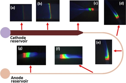
In anionic ITP, both sample proteins were negatively charged at the running pH and migrated from cathode to anode. Representative images of ITP migration at various regions of a 1D gradual reduction U shaped microchip are shown in Fig. 7. Protein bands were narrow and obscure initially at Fig. 7a, but as the bands progressed they accumulated mass and became wide and bright (Fig. 7b). A slight distortion of protein bands occurred in the reducing union and dispersion of bands were observed in the curved region of the microchannel (Figs. 7d, 7f). This kind of distortion23 and dispersion24 are normal; however, they were eliminated by ITP’s self-sharpening effect at sufficient distances from the reduction or curve. A final image prior to the anode reservoir showed that proteins formed three distinct bands (Fig. 7g).
Figure 7.
Time series photos of stacked proteins during anionic ITP in a 1D gradual reduction U-shaped PMMA microchip. The width of the channel varies with location, but the depth of the channel is kept constant at 10 μm as shown in the Fig. 1(a). (a) The proteins are beginning to stack out but are difficult to distinguish. (b) The proteins continue to accumulate mass and are migrating towards the gradual reduction region. (c) Slight distortion of proteins band occur in the gradual reduction region. (d)-(f) Proteins are in the curved region where small dispersion of protein bands occur at (d) and large dispersion happens at the end of this region (f). (g) The proteins are at the end of the channel, all distortions including dispersion in protein bands have been eliminated due to ITP’s self-sharpening effect.
We also quantified the concentration intensification by the ITP process presented here. The final concentration of proteins can be calculated from a simple mass balance equation as,
| (1) |
where is the concentration of ith protein, is the mass load of the ith protein, is the width of the ith protein band, and A is the cross sectional area of the ITP channel. Therefore, a 1D step reducing microchip shown in Figure 1a should be able to provide 10 fold additional concentration than that of a straight channel ITP as long as ITP is in the peak mode operation.
To find the final concentration of proteins from Eq. 1, one has to determine the protein band width. The peak (band) width of proteins is then calculated using moment analysis followed by variance calculation. The nth moment () is given by,25
| (2) |
where c(x) is the intensity value, x is the spatial position, and a and b are the limits of integration. Next the peak (band) width of the proteins is obtained from where,
| (3) |
and , , and are the zeroth, first, and second moment, respectively. Using Eqs. 1, 3, final concentration of PE, GFP, and cTnI were calculated to be ∼57.54 mg/ml, 19.18 mg/ml, and 48.87 mg/ml, respectively. The corresponding concentration factors were 1150, 380, and 280, respectively. The concentration factor was higher than expected for PE, but the concentration factors were very close to their theoretical limits for the GFP and cTnI.
Cationic ITP experiments
Cationic ITP was performed in the 2D gradual reduction cascade microchip. The channel was pressure-filled with the LE from the cathode reservoir to the anode reservoir. The sample solution was then injected into sample reservoir and pressure-filled into the separation channel through the tee channel. Due to lower microfluidic resistance, the mixture of samples travelled towards anode reservoir and displaced the LE. Thus, the region between the sample reservoir and the anode reservoir was filled with the mixture of samples and the LE in this region was flushed out of this section of the channel to the anode reservoir. Next, the anode reservoir was rinsed and then filled with the TE. Like previous experiments, the loaded chip was then mounted underneath the 5× objective lens of a Leica DM 2000 fluorescence microscope, and a constant voltage of 400 V was applied across anode and cathode reservoir and photos were taken with a camera.
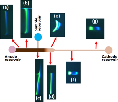
In cationic ITP both sample proteins were positively charged at the running pH, and, hence under the action of an electric field they migrated from the anode to the cathode. Initially, the proteins started to stack out and form bands, but they were very difficult to visualize and distinguish by the camera. Representative images of ITP as the protein bands progress through different regions of a 2D gradual reduction cascade PMMA microchip are shown in Fig. 8. In Figs. 8a, 8b, proteins bands have gathered enough mass to be clearly visible under the microscope. In Fig. 8c, the proteins have collected most of the total mass and are migrating through the T-junction. Slight distortion of bands was observed when they passed the T-junction and 2D gradual reduction region (Figs. 8c and 8e), and a gap between bands was observed after the gradual reduction region (Fig. 8f). Both gap between bands and distortion of bands were reduced as bands progressed further down the microchannel. Finally both proteins, FITC albumin and cTnI, stacked into distinct zones in the smaller cross-sectional area portion of the channel (Fig. 8g). However, there still exists a gap between proteins bands which might be due to unlabeled sample proteins or undissolved gases. Final concentration of pacific blue labeled cTnI and FITC albumin were found 11.0 mg/ml and 10.8 mg/ml, respectively, and corresponding concentration factors were ∼11 000 and ∼10 800, respectively.
Figure 8.
Time series photos of stacked proteins during cationic ITP in a 2D gradual reduction cascade PMMA microchip. The width and depth of the channel varies with location as shown in the Fig. 1b. (a) The proteins start to stack into ITP zones. (b) The ITP zones become brighter after accumulating more proteins. (c) The proteins have accumulated most of its total mass loaded onto the microchip. Some sample is lost due to migration through T-junction. (d) The proteins have passed the depth change region and protein bands become more easily visualized. (e) The proteins are passing through the width change and two distinct bands become brighter and wider. (f) The proteins are in the smallest cross-sectional area portion of the channel and the bands become more distinct with a gap between the two proteins. (g) The proteins are at the end of channel and have stacked into nearly pure zones.
CONCLUDING REMARKS
We have presented a new fabrication technique to form 2D gradual change SU-8 structure on various substrates. It has been found that PEI substrate has better adhesion with SU-8 than the conventional glass substrates, and the coefficient of thermal expansion of PEI makes it suitable substrate for hot embossing based PMMA microchip fabrication. Complex SU-8 structure can be easily fabricated on PEI substrate with multilayer photolithography. PMMA microchips can be created successfully by imprinting SU-8 features with hot press, and resulting channels can be enclosed with surface modification assisted bounding. This fabrication procedure is easy to implement, and it can be used for other plastics too. Although this fabrication technique has great promise, it has a few shortcomings too. First, in this fabrication technique, we do not have total control on the length of the 2D gradual change section of SU-8 structure. This length depends on the thickness of the SU-8 structure. Further research is required to get total control on the length of the 2D gradual change section. Second, for microdevice with branch channel(s) (as shown in Fig. 1b), it is very difficult to form multiple imprintings from a single SU-8 structure if the width of the branch channel is less than 100 μm. However, gradually increasing the branch channel width along the branch channel from its smallest value (100 μm or narrower) at the main channel junction can improve the number of successful imprintings. Nevertheless, microchips formed using the proposed microfabrication technique will reduce the overall cost, and hence this technique has commercial merits.
The performance of PMMA microchips fabricated using PEI substrate was demonstrated through cationic and anionic ITP experiments. The ITP experiments were started by applying a current through the separation channel. Thousand fold and ten-thousand fold increase in concentrations were observed when a 10× and 100× reduction in cross-sectional area microchannels were used for isotachophoretic preamplification.
ACKNOWLEDGMENTS
The research was supported by Washington state Life Science Discovery Fund and the Washington State University National Institutes of Health Protein Biotechnology Training Program Award Number T32GM008336 from the NIGMS. The content is solely the responsibility of the authors and does not necessarily represent the official views of the National Institute of General Medical Sciences or the National Institutes of Health.
References
- Piruska A., Nikcevic I., Lee S. H., Ahn C., Heineman W. R., Limbach P. A., and Seliskar C. J., Lab Chip 5, 1348 (2005). 10.1039/b508288a [DOI] [PubMed] [Google Scholar]
- Olabisi O., Handbook of Thermoplastics (Marcel Dekker, Inc., New York, 1997). [Google Scholar]
- Bhattacharya S., Datta A., Berg J. M., and Gangopadhyay S., J. Microelectromech. Syst. 14, 590 (2005). 10.1109/JMEMS.2005.844746 [DOI] [Google Scholar]
- Becker H. and Gartner C., Anal. Bioanal. Chem. 390, 89 (2008). 10.1007/s00216-007-1692-2 [DOI] [PubMed] [Google Scholar]
- Kricka L. J., Fortina P., Panaro N. J., Wilding P., Alonso-Amigo G., and Becker H., Lab Chip 2, 1 (2002). 10.1039/b109775j [DOI] [PubMed] [Google Scholar]
- Sun X. H., Peeni B. A., Yang W., Becerril H. A., and Woolley A. T., J. Chromatogr. A 1162, 162 (2007). 10.1016/j.chroma.2007.04.002 [DOI] [PMC free article] [PubMed] [Google Scholar]
- Koesdjojo M. T., Tennico Y. H., Rundel J. T., and Remcho V. T., Sens. Actuators B 131, 692 (2008). 10.1016/j.snb.2008.01.008 [DOI] [Google Scholar]
- Heckele M. and Schomburg W. K., J. Micromech. Microeng. 14, R1 (2004). 10.1088/0960-1317/14/3/R01 [DOI] [Google Scholar]
- Bahga S. S., Kaigala G. V., Bercovici M., and Santiago J. G., Electrophoresis 32, 563 (2011). 10.1002/elps.201000338 [DOI] [PubMed] [Google Scholar]
- Ge Z. W., Yang C., and Tang G. Y., Int. J. Heat Mass Transfer 53, 2722 (2010). 10.1016/j.ijheatmasstransfer.2010.02.033 [DOI] [Google Scholar]
- Dolnik V., Deml M., and Bocek P., J. Chromatogr. 320, 89 (1985). 10.1016/S0021-9673(01)90483-2 [DOI] [PubMed] [Google Scholar]
- http://www.microchem.com/pdf/SU-8-table-of-properties.pdf; see adhesion-shear analysis table for adhesion strength of SU-8 with silicon and other substrates.
- May G. S., Han S., and Hong S., Trans. Electr. Electron. Mater. 6, 135 (2005). 10.4313/TEEM.2005.6.4.135 [DOI] [Google Scholar]
- Bubendorfer A., Liu X. M., and Ellis A. V., Smart Mater. Struct. 16, 367 (2007). 10.1088/0964-1726/16/2/015 [DOI] [Google Scholar]
- Chiang Y.-M., Bachman M., Chang H.-P., Chu C., and Li G. P., in Materials Research Society Symposium Proceedings (Material Research Society, Warrendale, PA, 2000), pp. 91–96.
- Tennico Y. H., Koesdjojo M. T., Kondo S., Mandrell D. T., and Remcho V. T., Sens. Actuators B 143, 799 (2010). 10.1016/j.snb.2009.10.001 [DOI] [Google Scholar]
- John L. S.-J. and Narayan S., Microfabrication for Microfluidics (Artech House, INC., Norwood, MA, 2010). [Google Scholar]
- Moresco J., Clausen C. H., and Svendsen W., Sens. Actuators B 145, 698 (2010). 10.1016/j.snb.2010.01.020 [DOI] [Google Scholar]
- Shim J., Dutta P., and Ivory C. F., Numer. Heat Transfer, Part A 52, 441 (2007).
- Cui H. C., Dutta P., and Ivory C. F., Electrophoresis 28, 1138 (2007). 10.1002/elps.v28:7 [DOI] [PubMed] [Google Scholar]
- Bottenus D., Jubery T. Z., Ouyang Y. X., Dong Y. X., Dutta P., and Ivory C. F., Lab Chip 11, 890 (2011). 10.1039/c0lc00490a [DOI] [PMC free article] [PubMed] [Google Scholar]
- Khurana T. K. and Santiago J. G., Lab Chip 9, 1377 (2009). 10.1039/b815460k [DOI] [PubMed] [Google Scholar]
- Slais K., Electrophoresis 16, 2060 (1995). 10.1002/elps.v16:1 [DOI] [PubMed] [Google Scholar]
- Paschkewitz J. S., Molho J. I., Xu H., Bharadwaj R., and Park C. C., Electrophoresis 28, 4561 (2007). 10.1002/elps.v28:24 [DOI] [PubMed] [Google Scholar]
- Shim J., Dutta P., and Ivory C. F., Electrophoresis 28, 572 (2007). 10.1002/elps.v28:4 [DOI] [PubMed] [Google Scholar]


