Abstract
This paper presents a novel technique for the integration of small CMOS chips into a large area substrate. A key component of the technique is the CMOS chip based self-aligned masking. This allows for the fabrication of sockets in wafers that are at most 5 µm larger than the chip on each side. The chip and the large area substrate are bonded onto a carrier such that the top surfaces of the two components are flush. The unique features of this technique enable the integration of macroscale components, such as leads and microfluidics. Furthermore, the integration process allows for MEMS micromachining after CMOS die-wafer integration. To demonstrate the capabilities of the proposed technology, a low-power integrated potentiostat chip for biosensing implemented in the AMI 0.5 µm CMOS technology is integrated in a silicon substrate. The horizontal gap and the vertical displacement between the chip and the large area substrate measured after the integration were 4 µm and 0.5 µm, respectively. A number of 104 interconnects are patterned with high-precision alignment. Electrical measurements have shown that the functionality of the chip is not affected by the integration process.
Index Terms: BCB, bonding, chip-specific integration, CMOS, interconnect, MEMS, packaging, planarization, SOG
I. INTRODUCTION
The integration of microfluidics, MEMS and electronics within a compact footprint can revolutionize the area of handheld sensors for bio-threat detection and personalized medicine. Furthermore, this integration has the potential to deliver new types of instrumentation that can enable the discovery of new physics at the nanoscale; thanks to the vast parallelism afforded by lithographic integration. The major hurdle in realizing this vision has been the co-integration of CMOS devices with sensors, actuators and microfluidics due to either incompatibility of scale or processing conditions.
Another important consideration in integrated biomedical devices is the cointegration of passive components for signal conditioning or the integration of heterogeneous die in the case of optoelectronic platforms. Unlike transistors, passive devices such as capacitors and inductors do not scale well, and can occupy valuable silicon real-estate raising die costs and lowering the yield. Furthermore, RF devices require careful tuning of passive characteristics that can often enable superior performance. By using a post-integration methodology, passive components can be integrated without the associated package parasitics.
Traditionally, packaging and interconnection of disparate chips are performed by laborious and expensive techniques such as wire, flipchip and tape-automated bonding [1]. The density of interconnects that can be achieved with these techniques is limited. To accomplish high-resolution and high-density integration, several system-in-package (SIP) methods have been proposed in the past few years. For example, high-density interconnect (HDI) technology by General Electric [1], [2], chip-level integrated interconnect (CL-I2) technology by Rodger et. al. [3], [4], bumpless build-up layer (BBUL) packaging by Intel [28], and self-aligned wafer-level integration technology (SAWLIT) by Sharifi et. al. [5]. All these technologies share a similar protocol for the integration of chips. First, chips are embedded in etched cavities in a carrier substrate. A passivation layer is then created on top of chips and carrier using a polymer material. At the end, chip-to-package interconnections are patterned by applying photolithography and metal etching or lift-off. However, none of the proposed technologies offers the formidable combination of microfluidic integration, and post-CMOS micromachining of the packaged CMOS circuitry. Furthermore, these technologies can suffer from low yield, poor die-to-die alignment accuracy, and lack of robustness.
We present here for the first time a versatile chip-specific integration technology (VCSIT) which is CMOS, MEMS and bio-compatible, and offers both robustness and very accurate alignment. By judicious choice of materials we have designed a platform that can easily support post-CMOS micromachining. We introduce a self-aligned process that enables a robust integration of the die and the wafer. Furthermore, our process can be easily extended to integrate multiple dies on the same wafer. This gives an alternative approach to 3D-integration for integrating logic and memory components in close proximity, while simultaneously mitigating heat dissipation issues that remain a problem for 3D integration [6], [7].
The paper is organized as follows: we first give a detailed description of our integration process using a foundry-fabricated CMOS chip in Section II. We then evaluate the electrical performance of the packaged chip in Section III. The advantages and capacity of our proposed packaging technology are elucidated in Section IV. We then summarize our contribution and discuss some future work in Section V.
II. VERSATILE CHIP-SPECIFIC INTEGRATION TECHNOLOGY (VCSIT)
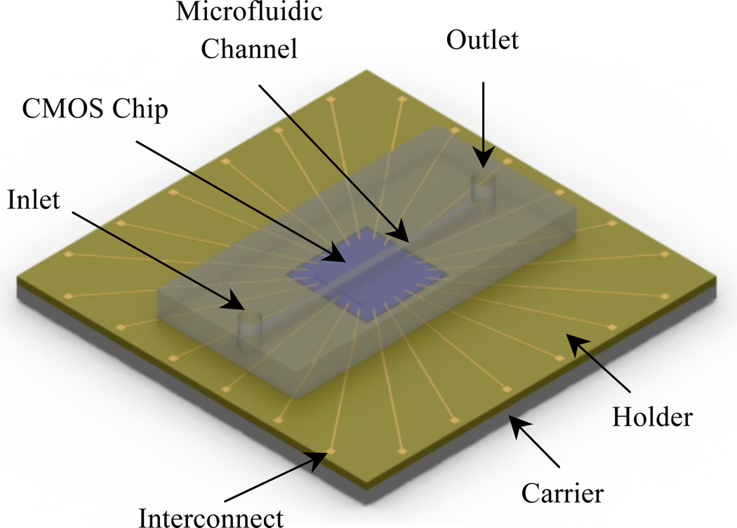
To demonstrate VCSIT, we used a CMOS chip, which is a low-power integrated potentiostat for biosensing, implemented in the AMI 0.5 µm technology. It is 3 mm × 3 mm × 260 µm in dimension, fabricated via MOSIS (Metal Oxide Semiconductor Implementation Service). The chip is integrated using two silicon substrates referred to as holder and carrier (Fig. 1). The holder serves as the housing for the chip. The holder and the chip are bonded onto a carrier by adhesive bonding using Benzocyclobutene (BCB). The top surface of the bonded chip and substrate is planarized by applying spin-on-glass (SOG). Interconnects leading from the chip to the holder are then patterned via a lift-off process. The schematic of a fully integrated biochip implemented using VCSIT is given in Fig. 1. The VCSIT process is elaborated in the following sub-sections.
Fig. 1.
Envisioned fully integrated biochip utilizing VCSIT
A. Chip Specific Cavity
The first step in the integration process is to create a cavity in a silicon holder where the CMOS chip will fit tightly. Chips obtained from different foundries can often vary in size by as much as 10–50 µm due to the thickness variation of the dicing saw that is used to dice the chips [5]. Hence, a single-size photomask cannot accommodate holes in the holder which are only a few micrometers larger on each side than individual chips. To resolve this issue, a chip-based lithography was implemented where individual chips are used as masks for photolithography to pattern holes.
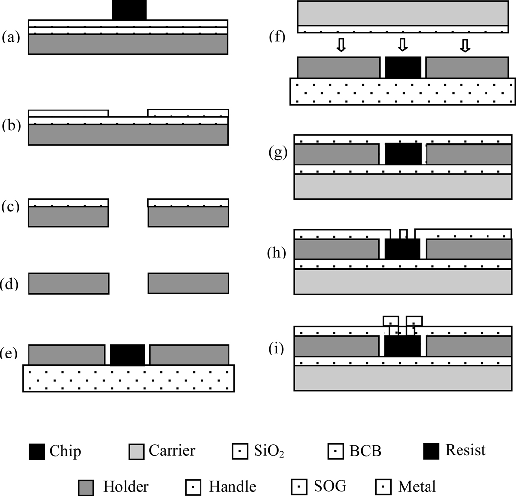
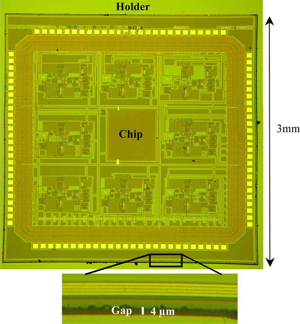
The process starts with the thermal oxidation (oxide thickness ~ 2 µm) of a 260 µm silicon wafer. The oxidized wafer is coated with the negative photoresist, AZ5214. A hole with the same size as the chip is then patterned in the resist by placing the chip on the resist-coated wafer, and using it as photomask (Fig. 2a, 2b). The pattern is then transferred to the oxide layer by an inductively coupled plasma (ICP) etch. Using the patterened oxide as a mask, a through-wafer hole is etched by a DRIE (deep reactive ion etch) Bosch process. (Fig. 2c). At the end, the oxide layer is removed by buffered hydrofluoric acid (Fig. 2d). Fig. 3 shows a microscopic top-view after the CMOS chip is placed inside the holder. The placement of the chip was done with the help of a flip-chip bonder. The gap between the holder and the chip was measured to be 4 µm.
Fig. 2.
VCSIT process steps to package a chip. (a) Chip is placed on the resist-coated, oxidized silicon holder. (b) A hole with the same size as the chip is patterned in the resist using the chip as photomask. (c) The pattern is transferred to the oxide layer, and through-holder etch is performed (d) Oxide on the holder is removed. (e) The holder and the chip are placed face-down on a handle substrate. (f) The BCB-coated carrier is bonded with the backside of the chip and the holder. (g) The gap between the chip and the holder is filled and the top surface is planarized with SOG. (h) Vias to the contact pads of the chip are created. (i) Metal interconnects from the chip to the holder are patterned.
Fig. 3.
Top-view of a CMOS die placed inside holder
B. Bonding
The second part of the integration process involves bonding the chip and the holder onto a carrier wafer. The carrier provides strong support and robustness to the packaged chip. Chips obtained from MOSIS usually have a rough surface on the backside due to back-grinding. Adhesive bonding is chosen for the bonding of holder and chip onto the carrier, since it requires no special substrate surface treatments such as planarization, chemical modifications, etc. In addition, adhesive bonding is robust, low-temperature, low-cost, and able to join heterogeneous substrates [8], [9].
Various materials are available to use as adhesives, e.g. BCB, SU8, polydimethylsiloxane (PDMS), polyimide, etc. The choice of a suitable adhesive for bonding is primarily based upon thermal and mechanical stability, and chemical resistance to acids, bases, or solvents to which it may be exposed to during subsequent fabrication processes. We chose BCB as the adhesive, since it offers a very high bond strength and excellent resistance to a number of strong chemicals. BCB is also known to be CMOS, MEMS and bio-compatible [8], [9], [10].
The bonding process starts with coating of the adhesion promoter, AP3000, on the carrier. This is followed by the spin-coating of a 7-µm thick layer of photosensitive BCB (Cyclotene 4024–40, Dow Chemical Company). BCB is precured at 100°C for 90 seconds. The precuring step prevents void formation from trapped air and out-gassing of solvent at the bond interface [8]. The holder and the chip are then positioned face-down on a handle wafer (Fig. 2e). The backside of the chip and the holder are coated with AP3000. The BCB-coated carrier is then flipped, and placed on the backside of the holder and the chip (Fig. 2f). The surfaces are bonded under pressure at elevated temperature in a Karl Suss SB-6 wafer bonder. The BCB carrier-holder interface is fully cured at 250°C in N2 ambient for an hour. A slow temperature ramp of about 1.5°C/min is used to reach the curing temperature of 250°C to reduce stress in the film.
The strength of the BCB bond was tested by harsh ultrasonic agitation, and further by cutting with a dicing saw. No delamination of the bonding interface has been observed.
C. Gap Filling and Planarization
In this part of the integration, the top surfaces of the chip and the holder are planarized in order to have a seamless transition from the chip to the holder. This is crucial for subsequent process steps such as patterning contacts from perimeter pads of the chip to the remote pads on the holder. Any discontinuity at the chip-holder interface will lead to broken metal lines and, thus, open circuits.
The critical aspect of the planarization step is to fill and bridge the high-aspect-ratio (HAR) gaps between the chip and the holder. High density plasma chemical vapor deposition of oxide has been the preferred method to fill gaps with aspect-ratios around 3. However, as the aspect-ratio increases, reliable gap-filling becomes increasingly difficult due to the void formation during the gap-filling process [12], [13]. A void-free and cost-effective method to fill HAR gaps is by using spin-on glass (SOG). Because of its low viscosity, SOG can easily reach the bottom of the narrow and HAR gaps, and completely fill them without voids while planarizing the surface [11], [14]. Hence, SOG (Accuglass 512B by Honeywell, Inc.) is chosen for our application.
A 0.8 µm SOG layer is coated on the bonded chip and holder by spinning SOG first at 150 rpm for 5 seconds, and then at 3000 rpm for 20 seconds. The dispensed volume of SOG for the coating is 1ml. The slow spin helps SOG to distribute itself uniformly and enter the gap between the chip and the holder, where as the higher spin speed planarizes the top surface (Fig. 2g). The gap-filling behavior of SOG during spin-coating is mainly due to the capillary effect. This capillary effect, and thereby the gap-filling performance, can be enhanced by raising the surface wettability [11]. Hence, before spinning SOG, the bonded chip and holder are treated with oxygen plasma (O2 flow rate 20 sccm, rf power 100W, chamber pressure 300 mTorr) for 5 minutes to improve the surface wettability. After the spin, SOG is soft-baked on a hot plate sequentially at 80°C, 150°C and 250°C, each for a minute. The same coating and curing process is repeated twice to ensure a complete gap-filling between the chip and the holder. At the end, the thick passivation layer that results from multiple coating is thinned down to 1 µm by ICP etch (CHF3 flow rate 20 sccm, ICP power 900 W, rf power 200 W, chamber pressure 0.5 Pa).
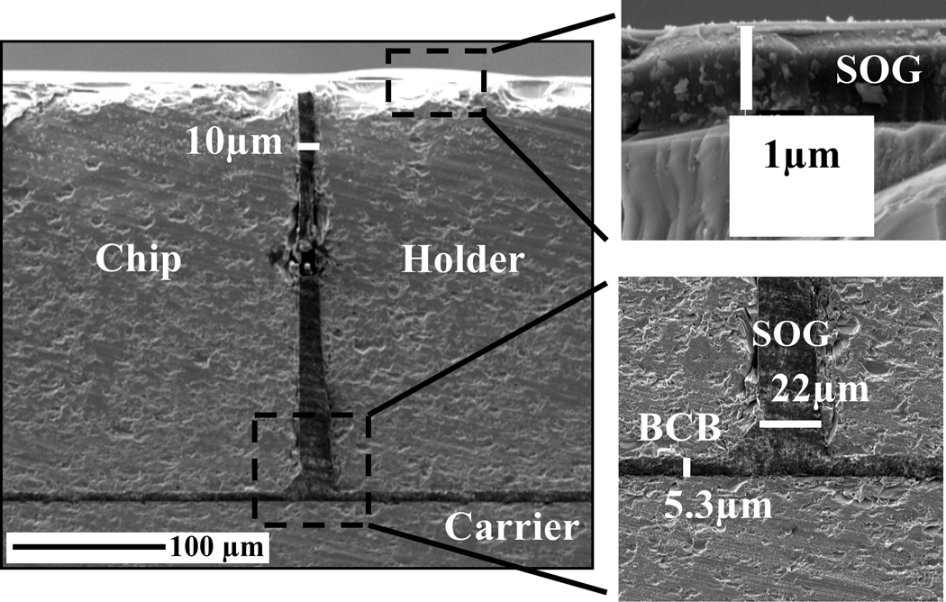
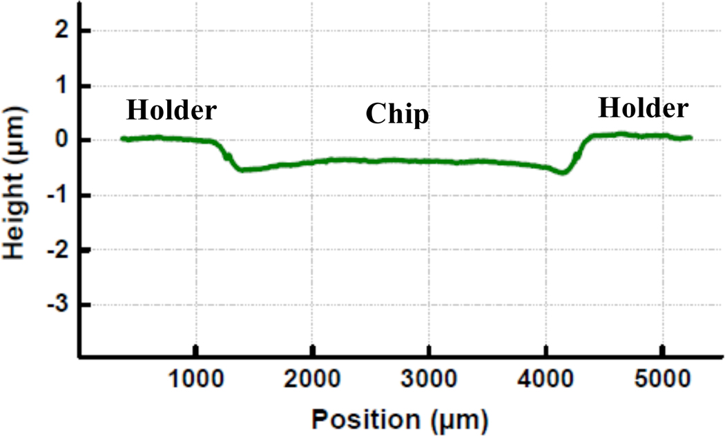
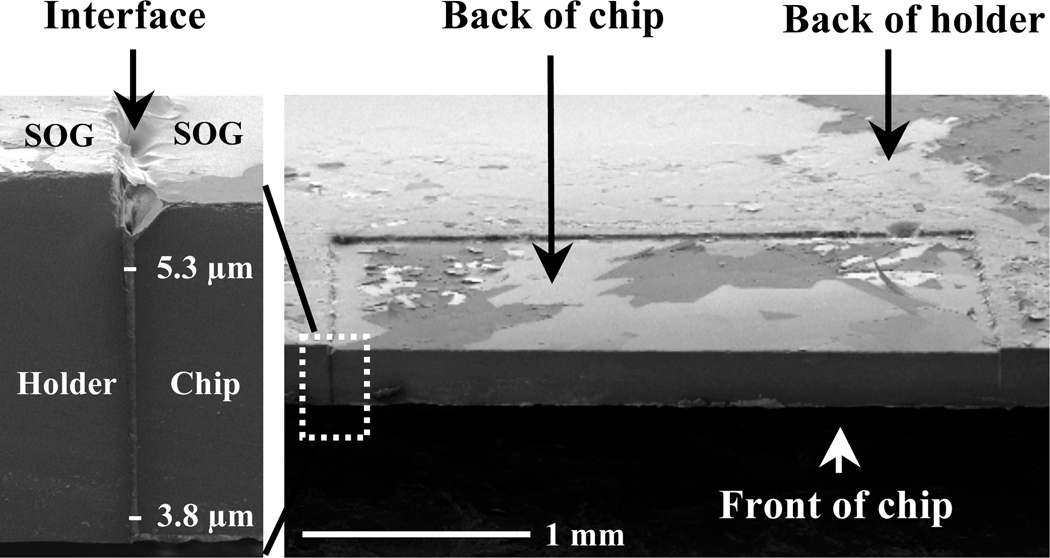
The SEM cross-sectional image of a packaged chip is given in Fig. 4. As seen from the figure, the gap between the chip and the holder is completely filled with SOG. The variation in gap size between top and bottom is due to the undercut profile resulting from the DRIE Bosch process. The difference in height between the chip and the holder is measured by a Dektak profilometer (Fig. 5). The vertical displacement of the chip relative to the holder is approximately 0.5 µm.
Fig. 4.
SEM cross-section of a packaged chip
Fig. 5.
Vertical displacement of an integrated chip relative to holder: The holder surface corresponds to 0-µm height.
D. Spin-on Glass Packaging
We have also implemented a simplified version of the integration scheme discussed in sub-sections A, B and C. The method obviates the use of a carrier wafer for the integration. After placing the chip and the holder face-down on a handle wafer, SOG is spin-coated three times on the backside of the chip and the holder (Fig. 6a, 6b). This results in complete gap-filling from the backside, and planarization of the bottom surface. The curing of SOG is performed on a hot plate sequentially at 80°C, 150°C and 250°C, each for a minute after each spin. The top surfaces of the chip and the holder are then planarized with SOG by following the same process as described in subsection C (Fig. 6c).
Fig. 6.
Process steps to integrate a chip using only SOG. (a) The holder and the chip are placed face-down on a handle substrate. (b) SOG is spun on the backside of the chip and the holder to fill the gap and planarize the bottom surface. (c) The handle substrate is removed, and the planarization is performed on the top surface of the chip and the holder.
The SOG film coated on top and bottom is found to be strong enough to hold the chip firmly inside the holder wafer during any subsequent process steps. Fig. 7 shows the SEM image of the backside of a chip that is integrated by applying the abridged packaging method. As seen from the figure, SOG planarizes the bottom surface of chip and holder with complete gap filling.
Fig. 7.
SEM image of the backside of a chip that was integrated using only SOG
E. Contact Pattern
In this part of the process, vias to the perimeter pads of the chip are created, and interconnect lines are patterned that extend from the chip to the holder.
Initially, contact vias are patterned by spinning resist and photolithographically opening the contact pads. Access to the aluminum pads are made by etching via holes in the SOG using the resist as a mask (Fig. 2h). The SOG is etched using CF4/O2(CF4/O2 flow rate 50 sccm/10 sccm, ICP power 200 W, rf power 50 W, chamber pressure 0.5 Pa).
After opening the contact vias, metal interconnects are patterned by applying lift-off of metal (Fig. 2i). First, the lift-off pattern is made by lithography using the negative resist, nLOF2070. A 500 nm aluminum layer is deposited on the top surface by electron beam evaporation. Metal lift-off is then performed in Shipley Microposit Remover 1165 at 80°C.
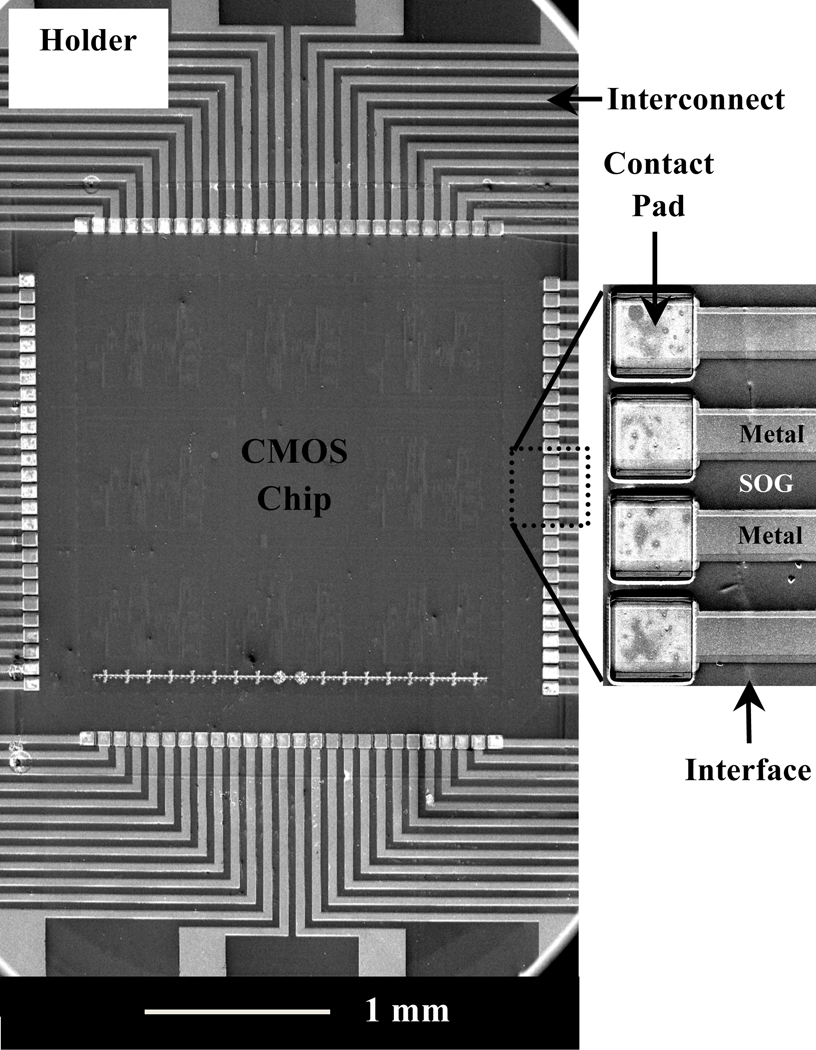
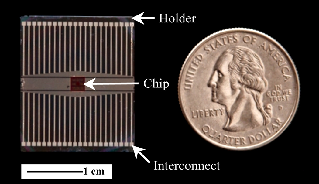
Fig. 8 shows the SEM image of interconnects on the packaged chip. A total of 104 interconnects are patterned from the chip to the holder. The interconnect line resistance is measured to be 4 Ω approximately. The contact pads of the chip are 78 µm × 78 µm, with a center-to-center pad distance of 90 µm. A photograph of the packaged chip is given in Fig. 9.
Fig. 8.
SEM micrograph of patterned interconnects
Fig. 9.
Image of a chip that was successfully integrated and post-processed
III. ELECTRICAL CHARACTERIZATION OF CIRCUIT
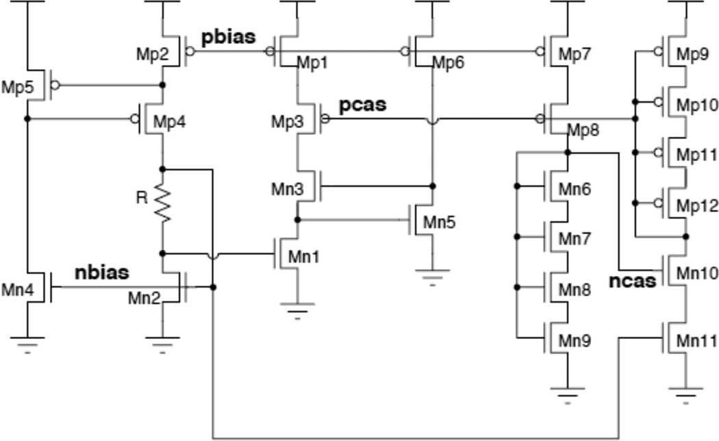
The effect of the integration process on the circuit performance has been evaluated. A key circuit in most analog processing blocks is a supply independent current source which serves as the ideal test circuit. One of the main reasons why this block serves as an ideal process indicator is that the bias voltages are directly proportional to process parameters, which are reflected in the unified parameter of threshold voltage. Threshold variations can cause functional failures, slower operating speeds or reduced dynamic range. A schematic of the supply independent current source is given in Fig. 10. The value of nbias can be calculated by equating the currents in transistors Mn1 and Mn2, and is given as follows.
| (1) |
where µn is the electron mobility, Cox is the gate oxide capacitance, Vgs is the gate-source voltage, Vtn is the threshold voltage of nMOSFET, L and W are the length and width of the device channel, and R is the resistance. The circuit forces a Vtn referenced nbias voltage by the action of a self-biased negative feedback loop. The pbias voltage is due to the action of a diode connected PMOS device and hence is Vtp referenced. Thus by measuring these voltages we can infer the effect of the process on the CMOS device parameters. In addition to measuring the nbias and pbias voltages, we also measured the cascode transistor (common-gate gain boosting) bias voltages, ncas and pcas to further validate the measurements.
Fig. 10.
Supply independent current source circuit of the CMOS chip
Table I shows the parameter values of the circuit measured on a bare die and an integrated die. For comparison purposes, values from a packaged chip by MOSIS are also included. As seen from the table, the measurements of the packaged and unpackaged chips match very well. After the integration the values of pbias and pcas have larger differences than the nbias and ncas measurements. However, since there is only one Vdd and Gnd pad on this particular chip, and given that 10 mA current is drawn from the supply by the chip, a total interconnect trace resistance between Vdd and Gnd of 8 Ω yields a total IR drop of 80 mV. This supply drop only affects pbias and pcas and not nbias and ncas. This was verified by measuring the bias voltages for various Vdd supplies, as given in Table II. Making the appropriate corrections yields a very modest difference between the bare and integrated dies, demonstrating that the process does not affect the circuit parameters.
TABLE I.
Test results of bare and integrated dies at Vdd = 5V
| pbias | pcas | ncas | nbias | |
|---|---|---|---|---|
| Unpackaged chip (V) | 3.648 | 3.197 | 1.844 | 1.383 |
| MOSIS Packaged chip (V) | 3.648 | 3.215 | 1.826 | 1.376 |
| Integrated die meas. 1 (V) | 3.547 | 3.124 | 1.846 | 1.374 |
| Integrated die meas. 2 (V) | 3.542 | 3.129 | 1.841 | 1.378 |
| Integrated die meas. 3 (V) | 3.544 | 3.128 | 1.842 | 1.371 |
| Integrated die meas. avg. (V) | 3.544 | 3.127 | 1.843 | 1.374 |
| Supply current (mA) | 10.00 | 10.00 | 10.00 | 10.00 |
| Trace resistance (Ω) | 8.00 | 8.00 | 8.00 | 8.00 |
| Supply IR drop (V) | 0.08 | 0.08 | 0.08 | 0.08 |
| Effective bias (V) | 3.624 | 3.207 | 1.843 | 1.374 |
| Difference voltage (V) (Bare die vs. Integrated die) | 0.024 | −0.010 | 0.001 | 0.009 |
TABLE II.
Test results of integrated dies at different Vdd
| Vdd (V) | pbias (V) | pcas (V) | ncas (V) | nbias (V) |
|---|---|---|---|---|
| 5 | 3.544 | 3.127 | 1.843 | 1.374 |
| 4 | 2.552 | 2.137 | 1.777 | 1.315 |
| 3 | 1.558 | 1.165 | 1.758 | 1.3 |
IV. DISCUSSION
VCSIT offers a number of important advantages over other SIP technologies reported before. For example, MCM and SAWLIT used top passivation layers of thickness, 25 µm and 6 µm, respectively [1], [5]. Vias to metal pads are then created by patterning the passivation layers. A thick passivation layer, and as a result deep vias, necessitates the deposition of a thick metal layer to ensure complete step coverage for making metal interconnects from chip to substrate. On the other hand, the micron thick passivation layer achieved with VCSIT results in a small step height from the metal pads to the top surface of the chip. In our case, the step height was 2.8 µm including the thickness of the passivation layer. Although thicker metals can be deposited for higher current applications, it is found that the deposition of even a relatively thin metal layer (200 nm) is sufficient to cover this via step completely. More importantly, the resulting thin passivation layer is less prone to introducing misalignment during the contact lithography due to the tight gap between the mask plate and the chip surface. Thus, VCSIT has considerably higher alignment accuracy in subsequent lithographic steps.
In VCSIT, chips are positioned in a self-aligned manner as a result of the tight gap that exists between the chip and the wafer. Thus the margin of misalignment is very small (few micrometers) during the placement of the chip. The SAWLIT process can only integrate chips which are of the same size. In this process, the chip housing in the holder wafer was about 10 µm larger on each side of the chip. Substantial optimization of the DRIE process was required to achieve the 10-µm gap. On the other hand, the chip based lithography technique of VCSIT is not only able to accommodate for the variation in chip size, but also to create the gap size as small as 4 µm without any optimization of the DRIE process. It is possible to make the gap even smaller with further optimization, thereby increasing the precision in chip alignment. High-accuracy alignment is critical for the integration of multiple dies in a large holder, especially to achieve ultra-high lead-count interconnects.
Earlier SIP technologies used PDMS, SU8, Polyimide, Parylene C, etc. for planarization or gap-filling [1]–[5]. All these polymers possess many attractive features: biocompatibility, low dielectric constant, flexibility, ease of processing, etc. However, some drawbacks are associated with these polymers which make them incompatible with either biological, CMOS or MEMS platform. PDMS has a low thermal conductivity and to maintain its chemical and physical properties, the temperature cannot exceed 200°C. Hence PDMS should not be used for applications where heat dissipation is critical, or operating temperature goes above 200°C [5]. In addition, PDMS is not compatible with non-polar and less-polar solvents such as acetone, chloroform, ether, etc., since these solvents diffuse into PDMS and cause it to swell [15]. SU-8 suffers from crack formation during the post-exposure bake due to the cross-linking of SU-8. Due to the mismatch of the coefficient of thermal expansion between SU-8 and substrate, internal stress is induced in the resist and bowing of substrate has been observed [16]. Polyimide has relatively high moisture uptake (4–6%). Some polyimides have lower moisture absorption, but they require high-temperature curing steps [3]. Parylene C has poor adhesion to underlying materials although an improvement in adhesion with a few materials has been demonstrated using an adhesion promoter [17]. SOG and BCB were chosen for planarization and bonding in VCSIT. SOG and BCB are widely used in the IC and MEMS industry as interlayer dielectric (ILD) [11], [18], passivation [22], [23], planarization [19], [20], and bonding materials [8], [21], because of their low dielectric constant, low-temperature process conditions and excellent chemical resistance. BCB is one of the preferred materials for biological applications since it has a very low moisture uptake (>0.2%) [10]. The excellent properties of BCB and SOG make VCSIT bio-, MEMS and post-CMOS compatible. However, random cracks were observed in the SOG film across the gap between the chip and the holder. This could be due to the thermal stress induced in thick SOG sandwiched between the chip and the holder [24]. The cracks were 100–300 nm wide. The cracks were filled by the plasma enhanced chemical vapor deposition of a 200 nm oxide layer.
The cost-effectiveness of VCSIT needs to be emphasized. Conventionally, space is allocated on the CMOS chip for the fabrication of large passive components and MEMS structures [25], [26]. Utilizing VCSIT, large passives and MEMS structures can be integrated with the packaged chip as disparate components by post-integration micromachining instead of on-chip fabrication. This can be achieved following a fabrication process similar to the one demonstrated by Rodger et. al. with their CL-I2 technology where off-chip RF-MEMS inductor coil is post-fabricated with the Parylene C encapsulated chip on the same platform [4]. Interconnects from the chip to the off-chip passives can then be patterned by standard photolithography. This will provide more integration flexibility, and decrease the complexity and cost of IC fabrication. Furthermore, the technology will facilitate the visual inspection of interconnects which is not possible in techniques such as flip-chip bonding [27].
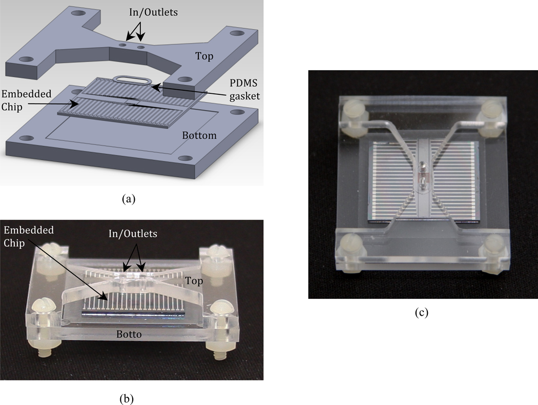
VCSIT facilitates the integration of fluidic channel on top of the CMOS chip. The footprint of the microfluidic systems usually exceeds the size of the CMOS chips. In order to facilitate the fabrication of microfluidic systems, the chip area needs to be increased to match the size of microfluidic systems. VCSIT offers a cost-effective way to increase the footprint by embedding the chip in a large substrate that serves as a platform for the subsequent fluidic integration. Fig. 11(b), (c) show a CMOS/Microfluidic hybrid system based on the VCSIT. The embedded chip is inlaid on an acrylic stage, and mechanically secured by fastening an acrylic microfluidic channel on top (Fig. 11(a)). A PDMS gasket is used to achieve a tight seal between chip and fluidic channel. After the integration of the fluidic channel, the pads of the CMOS chip can be accessed for electronic measurements via interconnect pads at the edge of the carrier. Various biosensing experiments are currently underway utilizing the proposed VCSIT microfluidics.
Fig. 11.
(a) Assembly of a CMOS/Microfluidic hybrid system. The VCSIT encapsulated chip is sandwiched between two acrylic parts where the fluidic channel lies in the top acrylic part. A PDMS gasket provides watertight seal between chip and fluidic channel. (b) Side-view and (c) top-view of the final CMOS/Microfluidic hybrid system.
VCSIT process can be easily extended to integrate multiple dies on the same wafer. The central issues with the multi-chip alignment are die-edge roughness due to the thickness of the dicing saw, and die placement accuracy. Die-edge roughness can be addressed following a process developed in [29] which involves deep reactive ion etch and ultra-precision grinding after initial dicing of chips. This process can achieve die-edge precision of 0.5 um. Such precision will allow us to use a fixed-size photomask for patterning cavities for multiple dies on the same wafer. The placement of each die can be achieved with a precision of 0.5um using a state-of-the-art bonder such as the Fineplacer Lambda die bonder from Finetech GmbH. Using these methods, die-to-die alignment accuracy within 2um and die-to-reference structure alignment within 1 um could be achieved. The free space between each die and holder needs to be greater than the combination of the die-edge precision, die-placement tolerance and lithographic tolerance for patterning the cavities.
V. CONCLUSION
A novel self-aligned chip-specific wafer level integration technology concept is presented. Due to the chip based lithography approach, the technique allows the creation of a very tight fit between the chip and the holder. The small vertical displacement between the chip and the holder, and the thin passivation layer on top allow for high-accuracy alignment during any post-integration fabrication processes. Thus, VCSIT has the potential to accomplish high-precision multichip integration with high-resolution, and ultra-high-density interconnects. In addition, the VCSIT platform has been designed with CMOS-, MEMS- and bio-compatible materials and processes. It allows for microfluidic integration and post-CMOS micromachining of the packaged chip. To validate the VCSIT, a low-power potentiostat CMOS chip was integrated using silicon substrates. High-density interconnects are patterned on top of the packaged chip. Electrical measurements on the supply current source of the chip show that the post-integration processing does not affect the CMOS device parameters.
Because of its versatility, the VCSIT promises to be a formidable approach to implement next-generation biochips, integrated CMOS RF IC’s and photonic CMOS chips.
ACKNOWLEDGEMENT
The authors gratefully acknowledge fruitful discussions with B. Thibeault and S. Beach, assistance with electrical measurements from N. Toledo and chip fabrication support from MOSIS, especially W. Hansford. Financial support from Intel Corporation and the National Institutes of Health through the NIH Director's New Innovator Award Program are also acknowledged. This work was done in the UCSB nanofabrication facility; part of the NSF funded the National Nanotechnology Infrastructure Network (NNIN).
This work was supported in part by Intel Corporation under Grant SB090065 and by the National Institutes of Health through the NIH Director's New Innovator Award Program, 1-DP2-OD007472-01.
Footnotes
Color versions of one or more of the figures in this paper are available online at http://ieeexplore.ieee.org.
REFERENCES
- 1.Daum W, Burdick WE, Fillion RA. Overlay high-density interconnect: A chips-first multichip module technology. Computer. 1993 Apr.vol. 26(no. 4):23–29. [Google Scholar]
- 2.Butler JT, Bright VM, Comtois JH. Multichip module packaging of microelectromechanical systems. Sens. Actuators A, Phys. 1998 Oct.vol. 70(no. 1/2):15–22. [Google Scholar]
- 3.Rodger DC, Tai YC. Microelectronic packaging for retinal prostheses. Engineering in Medicine and Biology Magazine, IEEE. 2005 Sept.–Oct.vol. 24(no. 5):52–57. doi: 10.1109/memb.2005.1511500. [DOI] [PubMed] [Google Scholar]
- 4.Li W, Rodger DC, Meng E, Weiland JD, Humayun MS, Tai YC. Wafer-Level Parylene Packaging With Integrated RF Electronics for Wireless Retinal Prostheses. Microelectromechanical Systems, Journal of. 2010 Aug.vol. 19(no. 4):735–742. [Google Scholar]
- 5.Sharifi H, Choi TY, Mohammadi S. Self-Aligned Wafer-Level Integration Technology With High-Density Interconnects and Embedded Passives. Advanced Packaging, IEEE Transactions on. 2007 Feb.vol. 30(no. 1):11–18. [Google Scholar]
- 6.Topol AW, Tulipe DCL, Shi L, Frank DJ, Bernstein K, Steen SE, Kumar A, Singco GU, Young AM, Guarini KW, Ieong M. Three-dimensional integrated circuits. IBM J. of Res. and Dev. 2006 Jul.vol. 50(no. 4/5):491–506. [Google Scholar]
- 7.Knickerbocker JU, Andry PS, Buchwalter LP, Deutsch A, Horton RR, Jenkins KA, Kwark YH, McVicker G, Patel CS, Polastre RJ, Schuster CD, Sharma A, Sri-Jayantha SM, Surovic CW, Tsang CK, Webb BC, Wright SL, McKnight SR, Sprogis EJ, Dang B. Development of next-generation system-on-package (SOP) technology based on silicon carriers with fine-pitch chip interconnection. IBM Journal of Research and Development. 2005 Jul.vol. 49(no. 4/5):725–753. [Google Scholar]
- 8.Niklaus F. Ph.D. Thesis. Stockholm, Sweden: Department of Signals; Sensors and Systems, Royal Institute of Technology (KTH); 2002. Adhesive wafer bonding for microelectronic and microelectromechanical systems. [Google Scholar]
- 9.Niklaus F, Griss P, Kalvesten E, Stemme G. Low-temperature wafer-level transfer bonding. Microelectro-mechanical Systems, Journal of. 2001 Dec.vol. 10(no. 4):525–531. [Google Scholar]
- 10.Lee K, Massia S, He J. Biocompatible benzocyclobutene-based intracortical neural implant with surface modification. J. Micromech. Microeng. 2005;vol. 15:2149–2155. [Google Scholar]
- 11.Byun K-M, Jung D-Y, Lee J-W, Lee S, Kim H, Kim M-J, Hong E, Gang M, Nam S-W, Moon J-T, Chung C, Lee J-H, Lee H-S. Robust spin-on glass gap-fill process technology for sub-30nm interlayer dielectrics. Interconnect Technology Conference (IITC) 2010 Jun.:1–3. [Google Scholar]
- 12.Bayman A, Rahman MS, Zhang W, Schravendijk BV, Gauri V, Papasoulitotis GD, Singh V. Gap fill for high aspect ratio structures. U.S. Patent 6 596 654. 2003 Jul. 22
- 13.Chen W, Wang S, Ashraf A, Somerville E, Nowaczyk G, Hwang BK, Lee JK, Moyer ES, Waldfried C, Escocia O, Han Q. A spin-on dielectric material for high aspect ratio gap fill. Mater. Res. Soc. Symp. Proc. 2005;vol. 863 [Google Scholar]
- 14.Hirasawa S, Saito Y, Nezu H, Ohashi N, Maruyama P. Analysis of drying shrinkage and flow due to surface tension of spin-coated films on topographic substrates. Semiconductor Manufacturing, IEEE Transactions on. 1997 Nov.vol. 10(no. 4):438–444. [Google Scholar]
- 15.Lee JN, Park C, Whitesides GM. Solvent Compatibility of Poly(dimethylsiloxane) Based Microfluidic Devices. Analytical Chemistry. 2003;vol. 75(no. 23):6544–6554. doi: 10.1021/ac0346712. [DOI] [PubMed] [Google Scholar]
- 16.Lorenz H, Laudon M, Renaud P. Mechanical characterization of a new high-aspect-ratio near UV-photoresist. Microelectron. Eng. 1998;vol. 41–42:371–374. [Google Scholar]
- 17.Hassler C, von Metzen RP, Ruther P, Stieglitz T. Characterization of parylene C as an encapsulation material for implanted neural prostheses. Journal of Biomedical Materials Research Part B: Applied Biomaterials. 2010;vol. 93B:266–274. doi: 10.1002/jbm.b.31584. [DOI] [PubMed] [Google Scholar]
- 18.Mills ME, Townsend P, Castillo D, Martin S, Achen A. Benzocyclobutene (DVS-BCB) polymer as an interlayer dielectric (ILD) material. Microelectron. Eng. 1997 Jan;vol. 33(no. 1–4):327–334. [Google Scholar]
- 19.Nezu H, Ohashi N, Tamaru T, Saikawa T, Owada N. Roadmap of SOG process for global planarization; IEEE Int. VLSI Multilevel Interconnection Conf; 1995. pp. 724–731. [Google Scholar]
- 20.Burdeaux D, Townsend P, Carr J. BenzoCycloButene (BCB) dielectrics for the fabrication of high density, thin film multichip modules. J. Electron. Mater. 1990 Dec.vol. 19(no. 12):1357–1366. [Google Scholar]
- 21.Lin HC, Chang KL, Pickrell GW, Hsieh KC, Cheng KY. Low temperature wafer bonding by spin on glass. J. Vac. Sci. Technol. B. 2002;vol. 20:752–754. [Google Scholar]
- 22.Chiu H-C, Yang S-C, Chan Y-J. Low-k BCB passivated Al0.5Ga0.5As/In0.15 Ga0.85As enhancement-mode pHEMTs; Gallium Arsenide Integrated Circuit (GaAs IC) Symposium, 23rd Annual Technical Digest; 2001. pp. 269–272. [Google Scholar]
- 23.Gaeta IS, Wu KJ. Improved EPROM moisture performance using spin-on-glass (SOG) for passivation planarization; International Reliability Physics Symposium; 1989. pp. 122–126. [Google Scholar]
- 24.Hashim U, Ayub RM. Characterization and optimization of inorganic spin on glass process for inter-metal dielectric using field emission scanning electron microscopy; IEEE International Conference on Semiconductor Electronics; 2002. pp. 485–489. [Google Scholar]
- 25.Fedder GK, Howe RT, Liu T-JK, Quevy EP. Technologies for Cofabricating MEMS and Electronics. Proceedings of the IEEE. 2008 Feb.vol. 96(no. 2):306–322. [Google Scholar]
- 26.Choi T, Lee H, Katehi LP, Mohammadi S. A low phase noise 10 GHz VCO in 0.18 µm CMOS process; Proc. Eur. Microw. Conf; 2005. Oct., pp. 273–276. [Google Scholar]
- 27.Harper CA. Electronic Packaging and Interconnection Handbook. New York: McGraw-Hill; 1991. [Google Scholar]
- 28.Towle SN, Braunisch H, Hu C, Emery RD, Vandentop GJ. Proc. ASME Int. Mech. Eng. Congress Exposition (IMECE) New York: 2001. Nov. 11–16, Bumpless build-up layer packaging. [Google Scholar]
- 29.Kommera S. Fabrication of Precise Die Edges for Micro-Optical and MEMS Applications. Advanced Packaging, IEEE Transactions on. 2007 Nov.vol. 30(no. 4):725–730. [Google Scholar]


