Abstract
Electronic systems that use rugged lightweight plastics potentially offer attractive characteristics (low-cost processing, mechanical flexibility, large area coverage, etc.) that are not easily achieved with established silicon technologies. This paper summarizes work that demonstrates many of these characteristics in a realistic system: organic active matrix backplane circuits (256 transistors) for large (≈5 × 5-inch) mechanically flexible sheets of electronic paper, an emerging type of display. The success of this effort relies on new or improved processing techniques and materials for plastic electronics, including methods for (i) rubber stamping (microcontact printing) high-resolution (≈1 μm) circuits with low levels of defects and good registration over large areas, (ii) achieving low leakage with thin dielectrics deposited onto surfaces with relief, (iii) constructing high-performance organic transistors with bottom contact geometries, (iv) encapsulating these transistors, (v) depositing, in a repeatable way, organic semiconductors with uniform electrical characteristics over large areas, and (vi) low-temperature (≈100°C) annealing to increase the on/off ratios of the transistors and to improve the uniformity of their characteristics. The sophistication and flexibility of the patterning procedures, high level of integration on plastic substrates, large area coverage, and good performance of the transistors are all important features of this work. We successfully integrate these circuits with microencapsulated electrophoretic “inks” to form sheets of electronic paper.
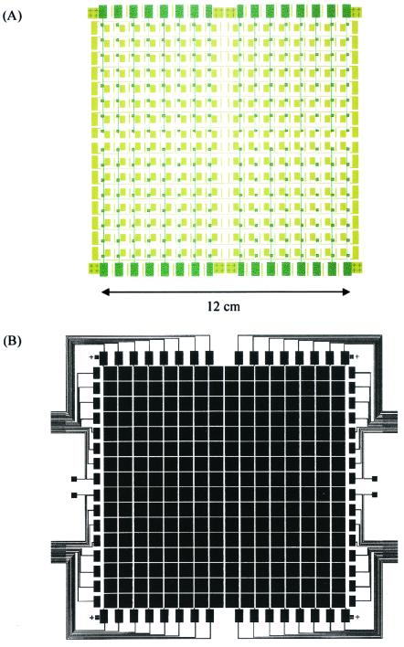
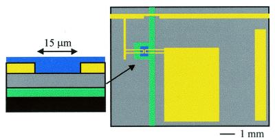
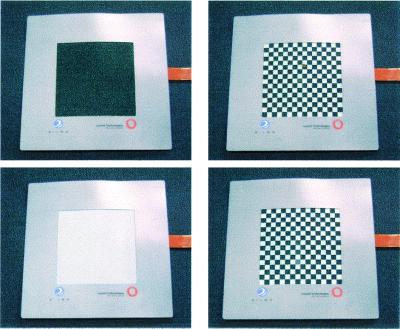
The backplane circuit consists of a square array of 256 suitably interconnected p-channel transistors. Fig. 1 shows the circuit layout. Fig. 2 presents a cross-sectional illustration of a transistor and a top view of a unit cell. The completed display (total thickness ≈1 mm) comprises a transparent frontplane electrode of indium tin oxide (ITO) and a thin unpatterned layer of flexible electronic “ink” mounted against a sheet that supports square pixel electrode pads and pinouts; these pixel pads attach, via a conductive adhesive, to the back planes. Each transistor functions as a switch that locally controls the color of the ink, which consists of a layer of polymeric microcapsules filled with a suspension of charged pigments in a colored fluid (1, 2). In each of the four quadrants of the display, transistors in a given column have connected gates, and those in a given row have connected source electrodes. Applying a voltage to a column (gate) and a row (source) electrode turns on the transistor located at the cell where these electrodes intersect. Activating the transistor generates an electric field between the frontplane ITO and the corresponding pixel electrode. This field causes movement of a pigment within the microcapsules, which changes the color of the pixel, as observed through the ITO: when the pigments flow to the ITO side of the capsules, the color of the pigment (white in this case) determines the color of the pixel; when they flow to the back, the pixel assumes the color of the dyed fluid (black in this case). Coordinated control of the transistors is achieved with external circuitry connected to the frontplane and to pinouts that lead to the column and row electrodes.
Figure 1.
(A) Layout of gate (green) and source/drain (yellow) levels of an active matrix backplane circuit for a sheet of electronic paper with 256 pixels. (B) Layout of pixel electrodes and pinout connections. The electrodes in B are bonded to a sheet that connects to the electronic ink on one side and to the backplane circuit on the other.
Figure 2.
Schematic illustration of the cross section of a display transistor and layout of a unit cell (blue, semiconductor; yellow, gold source/drain level; gray, dielectric; green, gate level; black, substrate). Each transistor controls the switching of electronic ink that lies above a pixel electrode that is electrically connected to the drain side of the transistor. The rectangle of gold on the right is generated by a raised support feature on the stamp that prevents mechanical sagging in the recessed regions during printing.
A transistor can switch a pixel (0.8 × 0.8 cm, resistance ≈75 MΩ) if it provides at least ≈1 μA of “on” current when the gate voltage (Vg) is −50 V and the source/drain voltage (Vsd) is −50 V. To avoid unwanted switching, the transistors must not produce more than ≈30 nA of “off” current when Vg = 0 V and Vsd = −50 V, or more than ≈30 nA of “leakage” current when Vg = −50 V and Vsd = 0 V. The driving scheme demands that the total capacitance associated with each pixel is sufficiently small to allow for millisecond switching times. (Although the refresh time of the entire display is ≈1 s, the pixels are switched in an approach that requires the transistors to operate at 250 Hz.) This requirement places limits on the area of overlap of the transistor channels and conductors on the source/drain level with the gate level. For the materials choices described in the following sections, channel widths (W) and lengths (L) that satisfy W/L ≈10 produce devices with comfortably more on and less off current than required. With 10-μm wires and L<≈20 μm, the overlap capacitance can be small enough for millisecond switching times.
Materials and Methods
Substrate, Gate, and Dielectric Levels.
Plastic substrates are critical components of electronic paper, because they enable the devices to be lightweight, mechanically flexible, and rugged. For the work described here, we used poly(ethylene terephthalate) (Mylar, 0.1 mm thick) for the substrate and ITO (≈100 nm thick) for the gate level (ITO-coated sheets of Mylar are commercially available from Southwall Technologies, Palo Alto, CA). Patterning a layer of etch resist on these substrates, followed by etching with concentrated hydrochloric acid (≈30 s), defines the features in the gate level. We demonstrated microcontact printing (μCP) (described below), conventional photolithography, and shadow masking to pattern these resists. Backplane circuits with gates formed by using each of these three methods showed identical performance.
A dielectric film deposited onto the patterned ITO insulates the gate and column electrodes from the other elements of the circuit. We used an organosilsesquioxane spin-on glass for this purpose, because (i) it can be spin cast into thin (<1 μm) films that show low electrical leakage, (ii) it can be cured at low (<150°C) temperatures, (iii) it is chemically compatible with a range of interesting organic semiconductors, and (iv) it can be used with etchants used in the μCP procedures described in the next section. To minimize the probability of electrical shorting between the source/drain level and the gate level and to reduce the leakage currents, we designed the circuit to avoid significant overlap of conductors and semiconductors with features of ITO or their edges. We also used films (≈0.8–1.0 μm) thick enough for low leakage but thin enough to enable sufficient on current. Their capacitance was between 2 and 10 nF/cm2. In some cases, we also used a thin (≈100 nm) layer of SiNx deposited at low temperatures (≈130°C) onto the ITO before casting the spin-on glass to increase the yield of devices with required on/off ratios and low leakage. (This material and the conditions for its deposition will be described elsewhere.)
Microcontact Printing and the Source/Drain Level.
The source/drain level typically demands features that are considerably smaller than those used for either the gate or the semiconductor. Even with the relatively large pixels in the display described here, the resolution (10–50 μm) required for the source and drain electrodes significantly exceeds the capabilities of current forms of (unassisted) ink jet printing (3, 4), screen printing (5, 6), and shadow masking (all of which have resolution ≈100–200 μm). Photolithography is not well suited for this application, partly because the photoresist and its processing are chemically incompatible with the spin-on glass dielectric. Photolithography also has other disadvantages: it is a relatively high-cost procedure that is challenging to use with large mechanically flexible plastic substrates.
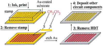
A low-cost rubber stamping technique known as μCP (7, 8) and a lithographic procedure based on molds and microfluidic channels (9, 10) are, to our knowledge, the only nonphotochemical approaches to patterning that have micrometer resolution and have been used to fabricate organic transistors. μCP is a particularly promising method that has the potential for patterning large areas quickly. It was first described by Whitesides and Kumar (7) and has since been explored by us and others for constructing simple devices in the areas of lasers (11), fiber optics (12), inorganic microelectronics (13–15), microfluidic analytical chemistry (16), and biotechnology (17). We recently reported processing conditions that enable μCP to be used for fabricating the source/drain level in a variety of basic organic electronic devices (8, 18–20). Fig. 3 outlines the general steps for using μCP to pattern electrodes for transistors that incorporate source/drain contacts beneath the semiconductor (i.e., bottom contact transistors). Casting and curing a prepolymer of polydimethylsiloxane (PDMS) against a surface with relief (i.e., a “master”) produces a rubber stamp with features in the geometry of those in the master. A single master can be used to generate many stamps, and each stamp can be used many times. A solution containing a molecular species that is capable of forming a self-assembled monolayer (SAM) (21) on the printing surface serves as the ink. The most well developed systems involve alkanethiol inks and copper, silver, or gold substrates. Thin gold electrodes are well suited to plastic electronic systems, because the gold is nonreactive and forms good electrical contacts with a range of organic semiconductors.
Figure 3.
Procedures for μCP source/drain electrodes for bottom contact organic transistors. Using a rubber stamp to print an ink of hexadecanethiol (HDT) yields a patterned SAM in the geometry of the stamp. Etching the gold that is not protected by the SAM produces a conducting circuit pattern. Removing the SAM facilitates electrical contact between these patterns and layers of organic semiconductor deposited on top of them.
A patterned SAM is generated simply by bringing the inked rubber stamp into contact with the gold for a few seconds. Etching the printed structure removes the gold not protected by the printed SAM. Removing the SAM exposes the bare gold and facilitates electrical contact with layers of organic semiconductors (8). In many cases, it is also possible to construct transistors by printing and etching gold films deposited on top of the semiconductor. We chose bottom contacts because the resulting transistors are mechanically robust: their electrodes are bound tightly to the dielectric rather than simply physisorbed onto the semiconductor.
The patterning component of the project described here builds on our initial work with μCP and plastic electronics by demonstrating methods for single-impression stamping over large areas with low levels of defects and good registration to existing features. These techniques and the good performance of the resulting circuits represent significant and important steps toward validating μCP as a means for constructing realistic systems. For the stamps, we used a large-area master formed in a thick layer (≈20 μm) of resist patterned by using a direct-write photolithographic system. To minimize the effects of thermal expansion, we cured the PDMS at room temperature. Stamps fabricated in this way shrink by only ≈0.25% (±0.05%), which is six times less than those cured in the usual way by heating at 65°C. For the 5 × 5-inch area of the display, even 0.25% shrinkage leads to registration errors that can be as large as ≈300 μm. The shrinkage, however, is uniform and isotropic to within <50 μm across the stamp, and it does not vary considerably from stamp to stamp. We therefore simply designed the gate and semiconductor levels to account for this 0.25% dimensional change.
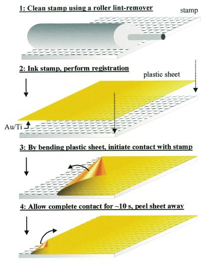
The spin-on glass/patterned ITO/Mylar substrates were prepared for μCP by depositing a thin layer of Ti (1.5 nm) as an adhesion promoter, followed by a film of Au (20 nm), by using an electron beam evaporator. Fig. 4 shows the approach that we used for large-area μCP. We first placed the stamp, printing side up, on a surface that allowed any residual elastic strains to relax (e.g., a thin layer of oil on a glass plate). Just before inking and printing, we cleaned the stamp by using a conventional roller lint remover. This simple procedure was extremely effective for quickly removing dust from the stamp without contaminating or damaging its surface. We then applied, with a pipette, a thin layer of a 2–3 mM solution of hexadecanethiol in ethanol over the entire surface of the stamp. After allowing this ink to remain on the stamp for a few seconds, we dried its surface with a stream of nitrogen. Matching crosshair alignment marks on the corners of one edge of the stamp with those patterned in the ITO brings the substrate into registration with the stamp. During this alignment, features on the stamp were viewed directly through the semitransparent substrate. By bending the Mylar sheet, we initiated contact with the stamp on the edge of the substrate that contained the crosshair marks. We then proceeded gradually to unbend the Mylar to allow contact to progress across the rest of the surface. This procedure for printing is attractive, because it avoids distortions that can arise from mechanical manipulation of the flexible rubber stamp during printing; it also minimizes the number and size of trapped air pockets. The few small bubbles that occasionally formed vanished in less than ≈30 s, as air diffused through the gas-permeable PDMS stamp. We typically allowed the substrate to remain in contact with the stamp for between 10 and 60 s.
Figure 4.
Procedures for using μCP to pattern over large areas, with low defects, low distortions, and good registration to existing features. The stamp is first placed, printing side up, on a surface that allows strains in the stamp to relax; the stamp is never directly manipulated again. A conventional roller lint remover removes dust from the surface of the stamp. After inking, registration marks on the plastic substrate are aligned with similar marks on the stamp. By gradually unbending the substrate, contact proceeds from the registered edge to the other in a manner that minimizes the formation of trapped pockets of air. Peeling the plastic sheet away from the stamp after maintaining contact for ≈10 s completes the printing.
The substrates were immersed in a ferri/ferrocyanide etching bath (22) [1 mM K4Fe(CN)6, 10 mM K3Fe(CN)6, 0.1 M Na2S2O3, 1.0 M KOH] shortly (<2 h) after they were printed. The etching proceeded, at room temperature and without agitation, for ≈12 min. We observed good pattern definition after etching for as little as 8 min (i.e., 8 min was sufficient to etch completely the unprinted regions of the 20-nm film of Au) or for as long as 18 min (i.e., there was no noticeable failure of the SAM resists during 18 min of etching). After etching, the samples were rinsed thoroughly with deionized water and were then immersed in a 1% solution of HF in water for ≈25 s to remove the exposed Ti. After another rinse with deionized water, the substrates were baked on a hot plate at 150°C for 2 h to remove the SAM. We visually inspected the printed patterns and, if necessary, repaired defects (typically fewer than 10 per circuit) by hand.
Depositing, Annealing, and Encapsulating the Semiconductor.
Depositing a semiconductor on top of the printed substrates yields a functional backplane circuit. We explored a range of organic materials for this purpose, including solution-cast regioregular poly(3-hexylthiophene) (p-type) (23) and evaporated films of pentacene (p-type) (24), α-sexithiophene (p-type) (25), dihexyl pentathiophene (p-type) (26), copper phthalocyanine (p-type) (27), and copper hexadecafluorophthalocyanine (n-type) (28). Experiments with these materials and a variety of device geometries and fabrication approaches showed that (i) for similar geometries, devices patterned with μCP have characteristics comparable to those of devices fabricated with a shadow mask, (ii) bottom contact devices have higher off currents and larger variations in their properties (both across a given substrate and with time in a given device) than top contact devices, and (iii) pentacene and certain other semiconductors can consistently yield stable bottom contact devices with high (>1,000) on/off ratios at voltages compatible with spin-cast dielectrics. In both bottom and top contact geometries, the mobilities derived from examining the characteristics of the printed transistors were comparable to those observed previously with SiO2 dielectrics and doped Si gates: in cm2/V s, they were approximately 0.002 for CuPc and F16CuPc, 0.01 for PHT, 0.04 for DH-α-5T, 0.005 for α-6T, and 0.1 for pentacene.
For the transistors in this display application, the mobility is not a particularly important characteristic of the semiconductor. The resolution provided by μCP allows the source/drain electrodes to be designed to produce transistors with large enough on currents and sufficiently small overlap capacitance, even with semiconductors that have low mobilities. Also, the current requirement to switch the electronic ink pixel is quite low, on the order of 0.5 μ/cm2. The challenging electrical requirement is the one imposed on the on/off ratio. We found that annealing the transistors (e.g., 100°C for ≈6 h in a nitrogen environment) after depositing the semiconductor enabled good uniform characteristics over the entire surfaces of the substrates. The primary effect of the annealing is to reduce the off currents (in some cases by more than 100 times); it also reduces transistor-to-transistor variations in the on currents. Annealed bottom contact devices had performance often as good as that of top contact transistors. To pattern the semiconductor, we used a metal shadow mask held against the substrates during deposition. This procedure restricted the coverage of the semiconductor to square regions centered at the transistor channels and away from the edges in the gate pattern. Finally, in some cases, we encapsulated the transistors with a thin (≈300 nm) layer of low-temperature SiNx. This procedure not only reduced the sensitivity of the transistors to the environment (e.g., encapsulated transistors functioned well, even when submerged in water and various organic solvents) but also reduced the off currents in annealed p-channel devices.
Results
Registration and Defect Density.
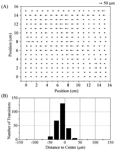
We carefully inspected several typical printed panels to quantify the registration with the gate level and to determine the density of defects. Fig. 5 illustrates the typical range of registration errors, as determined by examining the printed features with an optical microscope. The measurements define variations in the lateral distance between the center of each transistor channel and the midpoint between the edges of the gate pad that lie parallel to the channel width. The results show that (i) the overall alignment accuracy for positioning the stamp relative to the substrate (i.e., the offset of the center of the distribution of registration errors) is ≈50–100 μm, even with the relatively simple approach used here, and (ii) the (cumulative) distortions in the positions of features in the source/drain level, when referenced to the gate level, can be as small as ≈50 μm (i.e., the full width at half maximum of the distribution of registration errors). These results are remarkable, because they illustrate that small distortions can be achieved easily over large printed areas simply by avoiding direct mechanical manipulation of the stamp. It is likely that the relatively large distortions that have been observed in the past with μCP (29) were dominated by elastic strains induced by handling the stamps during printing. The printing approach illustrated in Fig. 4 is different from the usual method because it relies on contact established by bending a thin substrate that has a low flexural rigidity (which decreases like the cube of the thickness) but a relatively high in-plane Young's modulus (independent of thickness) rather than by bending the stamp, which has both low flexural rigidity and low in-plane Young's modulus. In fact, with this procedure, the stamp does not need to be flexible at all; it could, for example, consist of a thin layer of PDMS bonded to a rigid low thermal expansion glass support to reduce further the distortions and the shrinkage (29).
Figure 5.
Registration errors in a typical printed circuit, measured by using a microscope to examine the relative positions of features in the source/drain and gate levels. The results define variations in the lateral distance between the center of each transistor channel and the midpoint between the edges of the gate pad that lie parallel to the channel width. Both the overall positioning accuracy and the distortions easily meet the requirements for this application.
In addition to registration, we examined the density of electrically significant defects in the printed patterns. The results show that typically more than half of the flaws in the printed patterns originate from defects introduced in the photolithography used to produce the masters for the stamps. In all cases (i.e., μCP and photolithography), dust is the dominant cause of defects. (All processing was performed outside of a clean room in an open laboratory environment.) The simplicity and effectiveness of our approach to cleaning the stamp, which has no analog in the cleaning of conventional photomasks, as well as the ability of the stamp to conform to small dust particles, minimize their effects on the printed patterns.
Characteristics of the Circuits and the Displays.
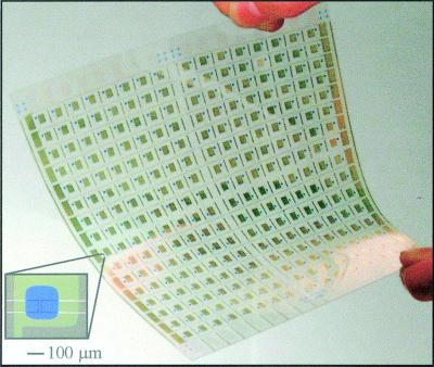
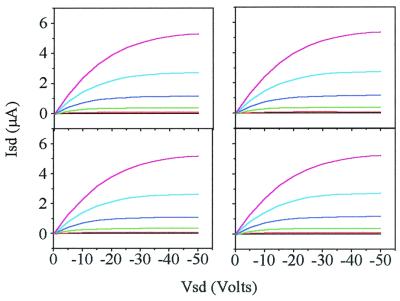
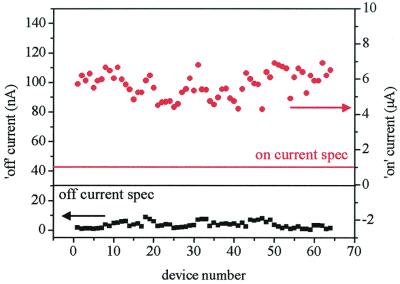
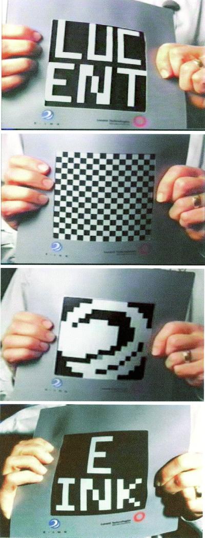
Fig. 6 shows an image of a full printed circuit; the Inset displays a micrograph of a transistor. To examine the performance and uniformity of the devices, we probed selected transistors by establishing gate and source contacts at the edges of the circuits and drain contacts at the corresponding unit cell. Fig. 7 shows, as an example, current–voltage characteristics in four randomly selected transistors. Fig. 8 presents on and off currents measured in 64 transistors. Although there is some variation in these properties, they all easily meet the electrical requirements for the display. Variations in the on currents have only slight effects on the switching times of the pixels. The display is monochrome (i.e., no gray scale) and the color of the pixels saturates at currents close to the ≈1 μA specification. Because the response of the pixels is nonlinear in the applied fields, off currents that fall below the specification have no effect on the display. Fig. 9 shows a completed sheet of electronic paper (total thickness ≈1 mm and contrast ratio >10:1, significantly better than that of newsprint) displaying images that demonstrate that all of the pixels are functioning well. Fig. 10 presents images of a display in operation while being flexed; the bending does not affect its performance. These displays operate on small battery packs that have lifetimes of several months of continuous use.
Figure 6.
Image of a completed plastic active matrix backplane circuit. The Inset shows an optical micrograph of a typical transistor.
Figure 7.
Current–voltage characteristics of several typical transistors in a rubber-stamped plastic backplane circuit. In each case, the gate voltage varied from 0 V to −50 V in steps of −10 V.
Figure 8.
On and off currents measured from 64 transistors in a printed backplane circuit. In all cases, the currents meet the required specifications. The on current is measured with Vsd = −50 V and Vg = −50 V. The off current is measured with Vsd = −50 V and Vg = 0 V. Leakage currents measured with Vsd = 0V and Vg = −50 V (not shown here) have magnitudes similar to the off currents.
Figure 9.
Sheet of electronic paper (total thickness, ≈1 mm) displaying several different images. The time for the display to switch from one image to another is ≈1 s.
Figure 10.
Sheet of electronic paper displaying images while being mechanically flexed. Bending does not alter the performance of the display.
Discussion
The work described in this paper demonstrates, that it is possible to print high-quality large-area plastic electronic systems on low-cost mechanically flexible polymer substrates. It shows, in particular, how rubber-stamped circuit elements can be combined with organic semiconductors to form active matrix backplanes for large sheets of electronic paper. The performance of these systems is excellent: (i) the transistors have characteristics (e.g., on and off currents, etc.) that are comparable to, or better than, those of similar devices fabricated on rigid silicon supports by using conventional photolithographic methods, and (ii) the optical characteristics (e.g., switching time, contrast ratio, etc.) of the resulting displays are as good as those of low-resolution signs that use similar electronic inks and direct-drive dressing schemes.
The fabrication sequences and materials combinations we discovered enable good properties, but we believe improvements are possible. In addition to straightforward engineering refinements (e.g., better control over materials purity, deposition conditions, etc.), a clear understanding of the basic chemistry and physics behind certain features we observed in these systems will be beneficial. For example, uncovering the mechanisms responsible for the pronounced differences between the electrical characteristics of top and bottom contact devices will almost certainly reveal routes to improving the transistors. In particular, the nature of semiconductor crystallization near the edges of bottom contact electrodes and the kinetics and thermodynamics of wetting at the triple interface between the semiconductor, the electrodes, and the gate dielectric are both potentially important. Also, the dramatic reduction in off current that follows encapsulation with SiNx appears worthy of further study. These and other observations illustrate a valuable feature of a focused effort like the one described here: the ability to reveal important basic research directions in a manner that can complement conventional laboratory experimentation.
Finally, we note that our work was motivated not only by our desire to identify essential scientific and engineering issues behind printing and plastic electronics, but also by our interest in establishing fabrication procedures and processing knowledge for devices with realistic features. Although our prototype displays do not have the number of pixels necessary for most consumer applications, many of the processing approaches can be extended to systems with more pixels and/or higher resolution. We are not aware, for example, of any fundamental obstacles that will prevent μCP and composite stamps from being effective at patterning the source/drain and gate levels on length scales of ≈1 μm with low-defect densities and registration to ≈5 μm. This resolution should easily allow for pixels with dimensions of ≈100 × 100 μm, the smallest size necessary for high-information-content electronic paper. Many of the materials used here also appear suitable for these high-resolution systems, although there may be some processing advantage to using electroless metal films and solution-cast semiconductors in place of vacuum-evaporated materials. Also, although our prototype displays have operated for 6 months in open laboratory conditions, additional work will be needed to ensure their long-term reliability in a range of temperatures and environments. Developing approaches to address these and other challenges will help to establish plastics as attractive alternatives to inorganics for certain types of electronic systems.
Acknowledgments
We thank Y.-Y. Lin for assistance with transistor characterization and P. Wiltzius, P. Drzaic, E. Reichmanis, and E. Chandross for helpful discussions.
Abbreviations
- PDMS
polydimethylsiloxane
- ITO
indium tin oxide
- μCP
microcontact printing
- SAM
self assembled monolayer
- Vg
gate voltage
- Vsd
source/drain voltage
Footnotes
This paper was submitted directly (Track II) to the PNAS office.
See commentary on page 4827.
References
- 1.Ota I, Ohnishi J, Yoshiyama M. Proc IEEE. 1973;61:832–836. [Google Scholar]
- 2.Comiskey B, Albert J D, Yoshizawa H, Jacobson J. Nature (London) 1998;394:253–255. [Google Scholar]
- 3.Hebner T R, Wu C C, Marcy D, Lu M H, Sturm J C. Appl Phys Lett. 1998;72:519–521. [Google Scholar]
- 4.Chang S C, Bharathan J, Yang Y, Helgeson R, Wudl F, Ramey M B, Reynolds J R. Appl Phys Lett. 1998;73:2561–2563. [Google Scholar]
- 5.Bao Z, Feng Y, Dodabalapur A, Raju V R, Lovinger A J. Chem Mater. 1997;9:1299–1301. [Google Scholar]
- 6.Garnier F, Hajlaoui R, Yasser A, Srivastava P. Science. 1994;265:1684–1686. doi: 10.1126/science.265.5179.1684. [DOI] [PubMed] [Google Scholar]
- 7.Kumar A, Whitesides G M. Appl Phys Lett. 1993;63:2002–2004. [Google Scholar]
- 8.Rogers J A, Bao Z, Makhija A. Adv Mater. 1999;11:741–745. [Google Scholar]
- 9.Kim E, Xia Y, Whitesides G M. Nature (London) 1995;376:581–584. [Google Scholar]
- 10.Rogers J A, Bao Z, Raju V R. Appl Phys Lett. 1998;72:2716–2718. [Google Scholar]
- 11.Rogers J A, Meier M, Dodabalapur A. Appl Phys Lett. 1999;74:3257–3259. [Google Scholar]
- 12.Rogers J A, Jackman R J, Wagener J L, Vengsarkar A M, Whitesides G M. Appl Phys Lett. 1997;70:7–9. [Google Scholar]
- 13.Deng T, Goetting L B, Hu J M, Whitesides G M. Sens Actuators A. 2000;86:122–126. [Google Scholar]
- 14.Jeon N L, Clem P, Jung D Y, Lin W, Girolami G S, Payne D A, Nuzzo R G. Adv Mater. 1997;9:891–894. [Google Scholar]
- 15.Rogers J A, Jackman R J, Whitesides G M. J Microelectromech Syst. 1997;6:184–192. [Google Scholar]
- 16.Rogers J A, Jackman R J, Whitesides G M, Olson D L, Sweedler J V. Appl Phys Lett. 1997;70:2464–2466. [Google Scholar]
- 17.Rogers J A, Jackman R J, Whitesides G M. Adv Mater. 1997;9:475–477. [Google Scholar]
- 18.Rogers J A, Bao Z, Dodabalapur A, Makhija A. IEEE Elect Dev Lett. 2000;21:100–103. [Google Scholar]
- 19.Tate J, Rogers J A, Jones C D W, Li W, Bao Z, Murphy D W, Slusher R E, Dodabalapur A, Katz H E, Lovinger A J. Langmuir. 2000;16:6054–6060. [Google Scholar]
- 20.Rogers J A, Bao Z, Meier M, Dodabalapur A, Schueller O J A, Whitesides G M. Synth Met. 2000;115:5–11. [Google Scholar]
- 21.Dubois L H, Nuzzo R G. Annu Rev Phys Chem. 1992;43:437–463. [Google Scholar]
- 22.Xia Y N, Zhao X M, Kim E, Whitesides G M. Chem Mater. 1995;7:2332–2337. [Google Scholar]
- 23.Bao Z, Dodabalapur A, Lovinger A J. Appl Phys Lett. 1996;69:4108–4110. [Google Scholar]
- 24.Gundlach D J, Lin Y Y, Jackson T N. IEEE Electron Device Lett. 1997;18:87–89. [Google Scholar]
- 25.Horowitz G, Fishou D, Peng X, Garnier F. Synth Met. 1991;41–43:1127–1130. [Google Scholar]
- 26.Li W, Katz H E, Lovinger A J, Laquidanum J G. Chem Mater. 1999;11:458–465. [Google Scholar]
- 27.Bao Z, Lovinger A J, Dodabalapur A. Appl Phys Lett. 1996;69:3066–3068. [Google Scholar]
- 28.Bao Z, Lovinger A J, Brown J. J Am Chem Soc. 1998;120:207–208. [Google Scholar]
- 29.Rogers J A, Paul K E, Whitesides G M. J Vac Sci Technol B. 1998;16:88–97. [Google Scholar]


