Abstract
The reasons for the relatively low transport mobility of graphene grown through chemical vapor deposition (CVD-G), which include point defect, surface contamination, and line defect, were analyzed in the current study. A series of control experiments demonstrated that the determinant factor for the low transport mobility of CVD-G did not arise from point defects or surface contaminations, but stemmed from line defects induced by grain boundaries. Electron microscopies characterized the presence of grain boundaries and indicated the polycrystalline nature of the CVD-G. Field-effect transistors based on CVD-G without the grain boundary obtained a transport mobility comparative to that of Kish graphene, which directly indicated the detrimental effect of grain boundaries. The effect of grain boundary on transport mobility was qualitatively explained using a potential barrier model. Furthermore, the conduction mechanism of CVD-G was also investigated using the temperature dependence measurements. This study can help understand the intrinsic transport features of CVD-G.
Graphene, a distinct two-dimensional (2D) building block, has attracted much attention due to its excellent transport properties that make it a promising material for next-generation nanoelectronics1,2,3,4. The strong interest in graphene has motivated various kinds of preparation methods, such as mechanical exfoliation from bulk graphite1, graphitization of silicon carbide substrate5,6, and chemical vapor deposition (CVD) on transition metals7,8,9. Among these methods, CVD method grown on polycrystalline copper foils exhibits its superiority from the relatively simple and low-cost growth, large size, predominant monolayer graphene growth, and ease of transfer to other substrates10. However, the charge carrier mobility of graphene grown through CVD (CVD-G) is typically orders of magnitude lower9 than the theoretical values11 or data reported for exfoliated graphene12,13. Clarifying the source of inferior carrier transport performance is highly desired for the realistic and industrial applications of CVD-G. Theoretical calculations in which graphene presents electronic excitations as two dimensional Dirac fermions predict the reasons may be led by impurities, edges and grain boundaries14,15,16,17,18,19. Combined with the experimental process from CVD-G growth to device fabrication, the main possible reasons for the inferior performance are suggested as point defect, surface contamination, and line defects. Although lateral experimental work36 also found the detrimental effect from above individual factor, the report systematically discussing the effect of above three factors is still absent especially unclear for the determined role among them. Considering further that the CVD-G growth does not grow slowly atom-by-atom from one nucleus, but rather through relaxation of a metal-carbon system with many nuclei20, the presence of defects in the as-grown CVD-G samples should be expected. Generally, point defect was introduced from damage effect, such as reconstruction to form nonhexagonal rings, particle irradiation to miss the lattice atom, carbon, or foreign adatom, and so on21,22,23,24; surface contamination was induced inevitably from the substrate transfer and device fabrication process12,13,25; meanwhile, line defect was mainly introduced by the grain boundary through the polycrystalline graphene materials26,27,28. Structural defects and surface contamination may act as internal or external scattering centers for electron waves, and greatly degrade transport properties25,26,27,28. Comparing to the vast amount of the available theoretical analysis, the experimental analysis to the transport of CVD-G has just begun, and especially for the lack of reproducible experimental results20.
To clarify the roles of the above three factors on CVD-G, various comparative experiments have been designed and carried out. Single crystalline graphene samples exfoliated from Kish graphite (Kish-G) was utilized as reference for the effect of point defect. Various contents of point defect were introduced into Kish-G samples through oxygen plasma bombardment. Thermal annealing treatment was adopted to remove surface contamination and to investigate its effect. Scanning electron microscopy (SEM), Transmission electron microscopy (TEM), and electrical transport measurements (room temperature and variable temperature dependence) were utilized to determine the presence and roles of grain boundaries. Results from the present investigation will be helpful to understand the origin of the transport properties of CVD-G.
Results
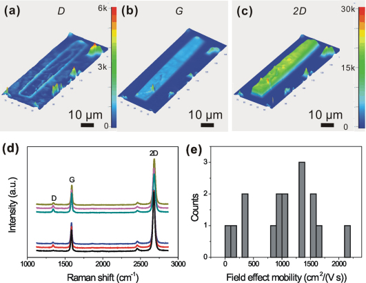
The structural and electrical properties of CVD-G samples have been investigated as shown in Fig. 1. Raman spectroscopy, a powerful tool to identify the presence of defects and graphene layers, was utilized to analyze the characteristics of Raman peaks. Three dimensional (3D) Raman maps of D, G, and 2D peaks from one typical CVD-G ribbon sample were extracted and plotted, as shown in Figs. 1a to 1c, respectively. The D peak, located at approximately 1350 cm−1, is caused by the breathing mode of sp2 atoms and activated by the existence of some defects such as edges, functional groups, or structural disorders30. The contrast of the D peak intensity in Fig. 1a clearly shows the defect spatial distribution. A pronounced D band signal was found on the edge of the sample which was introduced through patterning, while the continuous ridge, except for the edge, was resulted from the grain boundary. Thus, Raman mapping of the D peak intensity can provide a convenient way to identify the locations of the grain boundary. The maps of G and 2D are relatively uniform with high counts (approximately tens of thousands) except for few vertexes. The corresponding Raman spectra (Fig. 1d) were also extracted from six typical spots far from the edge. The intensity of the 2D peak is twice more than the intensity of the G peak. Furthermore, the shape of the 2D peak can be perfectly fitted by one Lorenz peak. Both of the above two Raman features assure the monolayer nature of the CVD-G samples30. The ratio of the intensity of the D peak to the intensity of the G peak (ID/IG) is conveniently utilized as the footprint for the estimation of the amount of defect in graphene. The corresponding ID/IG ratio as shown in Fig. 1d contains a small ratio varying from 0.02 to 0.15. The field effect mobility for CVD-G samples has been obtained from the back-gate FETs, which are mainly located at 800 cm2/(Vs) to 1700 cm2/(Vs), occupying 11 of the 16 measured devices. The mean mobility is approximately 1100 cm2/(Vs). The small ID/IG ratio and intermediate mobility demonstrated that our CVD-G was similar to previous results8,9,10 on CVD-G and could be utilized in control experiments, although its mobility was lower than that of the Kish-G (approximately 5000 cm2/(Vs)), as shown below.
Figure 1. Basic investigation of the CVD-G samples: (a–c) Intensity maps of the D, G, and 2D bands, respectively.
Figure 1b and c share the same count scale. (d) Raman spectra of the same sample as Fig. 1a to c were collected from six typical spots far from the edge. (e) Statistic field effect mobility distribution for CVD-G devices.
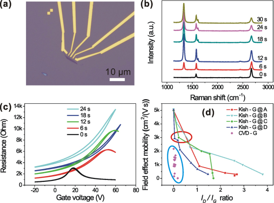
The presence of the defect has been captured in Raman map (Fig. 1a) which made it reasonable to correlate the defect to the lower transport mobility. Kish-G samples without the Raman defect signal were chosen as references to understand the effect of point defect. Figure 2a shows the optical image of a typical sample, Sample A of Kish-G (denoted as Kish-G@A). The point defect from particle irradiation has been introduced into Kish-G through oxygen plasma bombardment, and the content was controlled by increasing the exposure time. As shown in Fig. 2b, the ID/IG ratio increases as the exposure time extended from 6 s to 30 s. The increase of the ID/IG ratio indicates an evolution process from intact graphene lattice to a more disordered carbon phase. Figure 2c shows the corresponding electrical property evolution for plasma damage. The FET performance reveals a decrease in mobility and conductivity, as well as a positive shift in charge neutral point (CNP) voltage, indicating that p-dopants are attached to the defect sites31. Additional three devices (Sample Kish-G@B, C, and D) also displayed similar evolution trend through damage effect. The evolution curves of ID/IG ratio versus field effect mobility have been plotted based on Raman and electrical measurements (Fig. 2c). Although point defect has decreased the transport mobility of Kish-G samples (encircled by red oval) in a certain degree, Kish-G mobility is still higher (approximately twice) than that of CVD-G (encircled by blue oval) with similar point defect content. The interior transport mobility of CVD-G compared with that of Kish-G with similar ID/IG ratio suggested that point defect was not the main source of the low field effect mobility of CVD-G.
Figure 2. Damaged Kish-G samples as the references for CVD-G.
(a) Optical image for one typical Kish-G sample (Kish-G@A) with 1.6 μm channel length and 1.5 μm width; (b, c) Raman spectra and transfer character evolution as Kish-G@A is exposed to oxygen plasma with different duration time. (d) Mobility  versus ID/IG ratio for CVD-G and Kish-G samples, respectively.
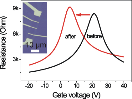
Graphene grown through CVD is generally integrated into devices via substrate transfer and electron beam lithography. The hydrophobic graphene surface was inevitably exposed to resist leading to the surface contamination which cannot be removed using standard solvents, such as acetone or remover12,13,25. Contamination may act as external scattering centers and degrade transport properties32. Thus, methods of cleaning the surface should be considered. Thermal annealing has been proven to be an efficient method to eliminate residue and restore the clean surface of graphene33,34. For that purpose, the CVD-G devices were thermally annealed under nitrogen gas protection. Figure 3 shows the transfer characteristic change of Device 1 via annealing treatment and the inset shows its corresponding optical image. After annealing, CNP decreased from 21 V to 6 V, which indicated that surface contamination was highly reduced35. Transport mobility was slightly reduced from 1370 cm2/(Vs) to 1090 cm2/(Vs). To eliminate exception from one device data, additional five devices have also been measured, and the corresponding key parameter change is listed in Table 1. Similar to the changing trend of Device 1, all the CNP voltages negatively shifted to 0 V and the mobility of most devices was kept with no considerable change. The exceptional one seriously decreased from one thousand to few tens may be damaged by coupling to the corrugated SiO2 surface13. The relatively clean CVD-G surface and little change in mobility assured that surface contamination was also not the main factor for low mobility.
Figure 3. Thermal annealing treatment to one CVD-G device (Device 1) and its corresponding optical image (inset).
The bottom center section is the working channel with 10 μm length and 5 μm width. The CNP decreased from 21 V to 6 V and the transport mobility was slightly degraded.
Table 1. Summary of the mobility and CNP change of CVD-G devices from the annealing treatment.
| Field effect mobility (cm2/(V s)) | Charge Neutral point (V) | |||
|---|---|---|---|---|
| Device No. | Before | After | Before | After |
| 1 | 1370 | 1090 | 20 | 6 |
| 2 | 1510 | 840 | 22.5 | 6.2 |
| 3 | 1040 | 40 | 26 | 11 |
| 4 | 1690 | 1640 | 24 | 13 |
| 5 | 1370 | 1250 | 27 | 4.8 |
| 6 | 900 | 2400 | 18 | −0.5 |
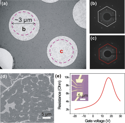
Aside from point defects and surface contamination, another possible source, namely, line defect, which mainly results from the grain boundaries or stacking faults is also very common in large area graphene sheet especially in CVD-G. To clarify the presence and roles of grain boundary, CVD-G samples were characterized using TEM, SEM, and FET measurements. Prior to the testing of SEM and TEM, more than 10 spots in a wide range distribution of CVD-G samples were tested by Raman to confirm the monolayer nature of our CVD-G30. Figure 4a shows the bright field TEM image of CVD-G. Two typical areas denoted by b and c (highlighted by pink dashed circles) were further tested using selected area electron diffraction (SAED), as shown in Figs. 4b and 4c, respectively. Figure 4b only contained one set of six-fold symmetric diffraction spots encircled by one white hexagon, indicating that the corresponding area was a single crystal grain with a diameter as large as 3 µm, whereas Fig. 4c was indexed as two sets of patterns (encircled by one red hexagon), which demonstrated that the viewing field was composed of two coalesced grains. The polycrystalline character of the CVD-G samples was further confirmed by stunting the growth of the CVD-G. An SEM image was obtained during the initial growth stage, as shown in Fig. 4d. Graphene simultaneously grew from the random nuclei (dark area with higher contrast compared with the white area from the uncovered metal surface) and finally merged with each other to form the large area polycrystalline sheet. The above growth process was consistent with the recent report36. The random distribution of the grain boundary causes difficulty in quantifying its effect on transport mobility. However, Raman mapping technique can help fabricate the device without the grain boundary. Prior to the device fabrication, the corresponding graphene ribbon was characterized by Raman mapping to confirm the absence of the grain boundary similar like Fig. 1a. Figure 4e was obtained from the short channel (approximately 2 μm in length) FET device without containing the grain boundary. The mobility of this kind of devices reached ∼2700 cm2/(Vs), which was comparative to the data from the Kish-G samples (∼3000 cm2/(Vs)) with similar defect content. The enhanced performance of CVD-G samples without grain boundary from the control experiments directly draw the conclusion that the determinant effect was from the grain boundaries.
Figure 4.
(a) Bright field TEM image of CVD-G, the pink dashed circle selected area denoted by b and c were further tested by SAED, corresponding to Fig. 4b and 4c, respectively. (b) The SAED pattern is composed of only one set of six-fold symmetric diffraction spots, highlighted by one white dashed hexagon, which indicates the single crystalline grain. (c) Two sets spots (circled by a red dashed hexagon), indicating that the viewing field is composed of two merged grains with small tilted angle. (d) SEM image of the paused growth sample. The higher contrast from the dark grains was divided by uncovered white metal surface. (e) Transfer characters for the short channel device (∼2 μm channel length and 1 μm width). The absence of grain boundary demonstrates the comparative transport mobility to Kish-G with similar defect content. Inset shows the corresponding optical image. The bottom center section is the working channel.
Although the precise mechanism of the transport mobility degradation led by grain boundary still remains elusive, what is known is that line defect promotes surface reactions with adsorbates from the ambient or with deposited dielectrics37. Substituting the network of hexagons with heptagons and pentagons in grain boundary has been observed experimentally, and quantum-transport calculations based on first principles have predicted that periodicity-breaking disorder can adversely affect transport properties38,39. The introduction of line defect can give rise to higher surface chemical activity that would further disrupt the sp2-bonding nature of graphene and thus, affect its fundamental properties. Therefore, the development of the growth method of large single crystal graphene is highly imperative to minimize the presence of line defect arising from boundaries between misoriented grains. The interior mobility performance mainly resulting from the grain boundaries was qualitatively explained using a potential barrier model40. The CVD-G is assumed to be composed of high and low resistivity areas. The high resistivity region works as the potential barrier, which is typically related to the grain boundaries, and separates the low resistivity area from each other. Assuming that the length, resistivity, and mobility for the low resistivity region (intra-grain) are  ,
,  , and
, and  , respectively, and the corresponding parameters for the higher resistivity region (inter-grain) are
  ,
,  , and
, and  , respectively, then the resistivity and the mobility for the whole CVD-G can be expressed as
  and
and  , where
  and
and  41. For typical conditions where,
  and
and  , the expression for the mobility can be simplified as
  . The introduction of the grain boundary, namely,
  increasing, the mobility of CVD-G obviously decreases according to the above expression. This conclusion is also consistent with the current CVD-G related experimental results.
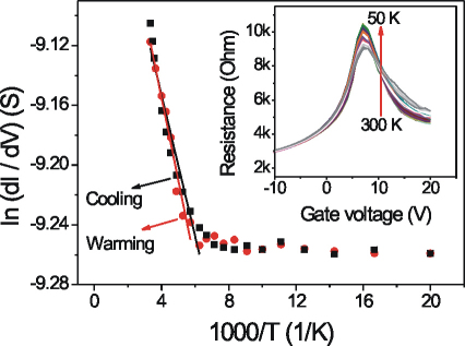
The charge transport mechanism of the polycrystalline CVD-G samples was investigated through temperature dependence conduction. Inset of Fig. 5 shows that resistance slightly increased after the sample cooling down and approximately 18% change had been obtained by varying the temperature from 300 K to 50 K. The plots for the minimum differential conductance versus temperature have been obtained (main panel of Fig. 5) through extrapolation. The small deviation between the cooling down and warming up processes shows the small hysteresis during temperature change. For the relationship between the natural logarithm of conductance versus 1000/T, it displays two distinct temperature dependent features. One is the temperature independent region at low temperature; the other is the linear temperature dependence in the high temperature region. In the low temperature part, the conduction of CVD-G is not like the insulator in which the conductance decreases as the temperature decreases. The most likely explanation for the observed temperature independent conduction at low temperature is tunneling42. Tunneling through grain boundary barriers requires no thermal excitations and can occur even at zero temperature, it exhibits a temperature independent conductance process. This kind of temperature independent conduction is analogous to the relatively large conductance in the zero-temperature limit often observed in high-conducting polymers and single-walled carbon nanotube networks43,44. While in high temperature part, the conduction deviates from the constant plateau and shows linear temperature dependence. It can be well fitted by a Arrhenius relation dI/dV∝exp(−Ea /2kBT)42, where Eais the activation energy and kB is the Boltzmann constant. The estimated activation energy from the Arrhenius equation is approximately 10 meV which describes the tunneling barrier height that the carriers overcome. Considering the adverse effect to the carrier transport induced by the grain boundary, the utilization of CVD-G in high performance electrical devices should decrease the content of grain boundary or even be absence of it.
Figure 5. Temperature dependence of CVD-G conduction.
Inset shows the transfer curves which vary as temperature changed. Plots from  show two distinct temperature dependent features, one keeps at a plateau in low temperature part and the other linearly changes at high temperature.
Discussion
In summary, the reasons for the relatively low transport mobility of CVD-G were investigated through a series of control experiments. The possible reasons were studied gradually to find its determinant factor. The higher transport mobility (approximately 3000 cm2/(Vs)) for damaged Kish-G compared with CVD-G (approximately 1100 cm2/(Vs)) with similar content of defect demonstrated that point defect was not the main source of low mobility. Although thermal annealing treatment could greatly reduce the CVD-G surface contamination, mobility was slightly degraded, which also indicated that surface contamination was not the key factor affecting mobility. Both of TEM and SEM characterizations demonstrated the polycrystalline nature of CVD-G growing from random multi-nuclei. The transport mobility of the short channel devices absent of the grain boundary can reach 2700 cm2/(Vs). This data was comparative to that of the Kish-G, in such defect degree. Combining SEM and TEM characterizations with the superior performance of the devices without grain boundary shows that grain boundary was the determinant factor for the inferior performance of CVD-G. A potential barrier model has been suggested to qualitatively explain the detrimental effect of grain boundary. Further temperature dependence conduction demonstrated that the charge transport mechanism was attributed to tunneling in the low temperature part and thermal activation in high temperature region. The unfolded origin of relatively lower transport mobility of CVD-G can help remove the block and promote the development of CVD-G.
Methods
The CVD-G samples grown on Cu foil/film utilized in the current study were prepared using the well-developed CVD technique and subsequently transferred to p-type heavily doped silicon substrate covered with 285 nm SiO2 in Reference9 and29. The experimental process can be described briefly as follows. Cu film sputtered on SiO2/Si substrates was placed in a cold wall type high-vacuum chamber using CH4 diluted by Ar and H2 as carbon source. After Ar/H2 annealing for 20 min, graphene growth was performed at 1000°C under a pressure of approximately 1 kPa for 60 min. For the paused growth samples, the growth time was decreased to 20 min, whereas the other parameters were kept constant. Thermal annealing treatment of CVD-G was conducted using a rapid thermal annealing furnace at 300°C for 30 min under nitrogen gas.
The reference Kish-G samples were prepared via mechanical exfoliation of Kish graphite on SiO2/Si substrate. Damage effect was introduced to Kish-G by applying low power (20 W) oxygen plasma with variable duration time to obtain the different contents of point defect. The corresponding Raman spectra and electrical measurements were performed in a short time interval (within 10 min) after the occurrence of the damage.
For device fabrication, the obtained graphene samples located on the SiO2/Si substrate were first patterned into regular geometry using oxygen plasma. Four terminal electrodes were then deposited on graphene using electron beam lithography followed by Ti/Au (5 nm/50 nm) evaporation and a lift-off process. Finally, back-gate field-effect transistors (FETs) were fabricated using a standard procedure. All Raman measurements were carried out under ambient atmosphere and temperature, whereas electrical measurements were performed under a four-terminal geometry in a sample-in-vacuum (approximately 5×10⁻⁷ mbar) cryostat with a temperature range of 50 K to 300 K.
Author Contributions
S.H.S and K.T. planned the experiments. S.S., K.H., A.Y., N.Y. fabricated the CVD-G and characterized it by SEM and TEM. H.S.S., S.L.L. and H.M. performed the oxygen plasma damaging, thermal annealing experiments and processing of the data. All authors contributed to the discussion of the results. S.H.S and K.T. wrote the paper.
Acknowledgments
H. S. S. gratefully acknowledges Dr. Michael Lee, Dr. Hiromi Kuramochi, Dr. Yun Li and Dr. Shu Nakaharai for their experimental help and useful discussions. This work was partly supported by JSPS through the FIRST Program, initiated by CSTP, Japan.
References
- Novoselov K. S. et al. Electric field effect in atomically thin carbon films. .Science 306, 666–9 (2004). [DOI] [PubMed] [Google Scholar]
- Geim A. K. Novoselov K. S. The rise of graphene. Nat. Mater. 6, 183 (2007). [DOI] [PubMed] [Google Scholar]
- Li S. L., Miyazaki H., Kumatani A., Kanda A. & Tsukagoshi K. Low operating bias and matched input-output characteristics in graphene logic inverters. Nano Lett. 10, 2357–2362 (2010). [DOI] [PubMed] [Google Scholar]
- Tang Y. B. et al. High-quality graphenes via a facile quenching method for field-effect transistors. Nano Lett. 9, 1374–7 (2009). [DOI] [PubMed] [Google Scholar]
- Deheer W. A. et al. Epitaxial graphene. Solid state Commun. 143, 92–100 (2007). [Google Scholar]
- Emtsev K. V. et al. Towards wafer-size graphene layers by atmospheric pressure graphitization of silicon carbide. Nat. Mater. 8, 203–207 (2009). [DOI] [PubMed] [Google Scholar]
- Chen Z. P. et al. Three-dimensional flexible and conductive interconnected graphene networks grown by chemical vapour deposition. Nat. Mater. 10, 424–8 (2011). [DOI] [PubMed] [Google Scholar]
- Kim K. S. et al. Large-scale pattern growth of graphene films for stretchable transparent electrodes. Nature 457, 706–710 (2009). [DOI] [PubMed] [Google Scholar]
- Li X. et al. Large-area synthesis of high-quality and uniform graphene films on copper foils. Science 324, 1312–1314 (2009). [DOI] [PubMed] [Google Scholar]
- Bae S. et al. Roll-to-roll production of 30-inch graphene films for transparent electrodes. Nat. Nanotechnol. 5, 574–578 (2010). [DOI] [PubMed] [Google Scholar]
- Morozov S. V. et al. Giant intrinsic carrier mobilities in graphene and its bilayer. Phys.Rev.Lett. 100, 016602 (2008). [DOI] [PubMed] [Google Scholar]
- Du X., Skachko I., Barker A. & Andrei E. Y. Approaching ballistic transport in suspended graphene. Nat. Nanotechnol. 3, 491–495 (2008). [DOI] [PubMed] [Google Scholar]
- Bolotin K. I. et al. Ultrahigh electron mobility in suspended graphene. Solid State Commun. 146, 351–355 (2008). [Google Scholar]
- Trushin M. Schliemann J. Minimum electrical and thermal conductivity of graphene: a quasiclassical approach. Phys. Rev. Lett. 99, 216602 (2007). [DOI] [PubMed] [Google Scholar]
- Yan X. Z., Romiah Y. Ting C. S. Electric transport theory of Dirac fermions in graphene. Phys. Rev. B 77, 125409 (2008). [Google Scholar]
- Kim E. A. & Castro Neto A. H. Graphene as an electronic membrane. EuroPhys.Lett. 84, 57007 (2008). [Google Scholar]
- Shishir R. S. & Ferry D. K. Intrinsic mobility in graphene. J. Phys: Condens. Matter. 21, 232204 (2009). [DOI] [PubMed] [Google Scholar]
- Ziegler K. Robust transport properties in graphene. Phys. Rev. Lett. 97, 266802 (2006). [DOI] [PubMed] [Google Scholar]
- Peres N. M. R., Guinea F. & Neto A. H. C. Electronic properties of disordered two-dimensional carbon. Phys. Rev. B 73, 195411 (2006). [Google Scholar]
- Banhart F., Kotakoski J. & Krasheninnikov A. V. Structural defects in graphene. ACS Nano 5, 26–41 (2011). [DOI] [PubMed] [Google Scholar]
- Stone A. J. & Wales D. J. Theoretical-studies of icosahedral C60 and some related species. Chem. Phys. Lett. 128, 501–503 (1986). [Google Scholar]
- Banhart F. Irradiation effects in carbon nanostructures. Rep.Prog.Phys. 62, 1181–1221 (1999). [Google Scholar]
- Tsetseris L. Pantelides S. T. Adatom complexes and self-healing mechanisms on graphene and single-wall carbon nanotubes. Carbon 47, 901–908 (2009). [Google Scholar]
- Banhart F. Interactions between metals and carbon nanotubes: at the interface between old and new materials. Nanoscale 1, 201–213 (2009). [DOI] [PubMed] [Google Scholar]
- Chen F., Xia J., Ferry D. K. & Tao N. Dielectric screening enhanced performance in graphene FET. Nano Lett. 9, 2571–4 (2009). [DOI] [PubMed] [Google Scholar]
- Coraux J. N., Diaye A. T., Busse C. Michely T. Structural coherency of graphene on Ir(111). Nano Lett. 8, 565–570 (2008). [DOI] [PubMed] [Google Scholar]
- Cervenka J., Katsnelson M. I. Flipse C. F. J. Room-temperature ferromagnetism in graphite driven by two-dimensional networks of point defects. Nat. phys. 5, 840–844 (2009). [Google Scholar]
- Lahiri J., Lin Y., Bozkurt P., Oleynik I. I. & Batzill M. An extended defect in graphene as a metallic wire. Nat. Nanotechnol. 5, 326–329 (2010). [DOI] [PubMed] [Google Scholar]
- Kondo D. et al. Low-temperature synthesis of graphene and fabrication of top-gated field effect transistors without using transfer processes. Appl. Phys. Express 3, 025102 (2010). [Google Scholar]
- Ferrari A. C. et al. Raman spectrum of graphene and graphene layers. Phys. Rev. Lett. 97, 187401 (2006). [DOI] [PubMed] [Google Scholar]
- Childres I., Jauregui L. A., Tian J. Chen Y. P. Effect of oxygen plasma etching on graphene studied using Raman spectroscopy and electronic transport measurements. New J. Phys. 13, 025008 (2011). [Google Scholar]
- Ishigami M., Chen J. H., Cullen W. G., Fuhrer M. S. Williams E. D. Atomic structure of graphene on SiO2. Nano Lett. 7, 1643–1648 (2007). [DOI] [PubMed] [Google Scholar]
- Dean C. R. et al. Boron nitride substrates for high-quality graphene electronics. Nat. Nanotechnol. 5, 722–726 (2010). [DOI] [PubMed] [Google Scholar]
- Nourbakhsh A. et al. Tuning the fermi level of SiO2-supported single-layer graphene by thermal annealing. J. Phys. Chem. C 114, 6894–6900 (2010). [Google Scholar]
- Tan Y. W., Zhang Y., Stormer H. L. & Kim P. Temperature dependent electron transport in graphene. Eur. Phys. J. Special topics. 148, 15–18 (2007). [Google Scholar]
- Yu Q. et al. Control and characterization of individual grains and grain boundaries in graphene grown by chemical vapour deposition. Nat. Mater. 10, 443–449 (2011). [DOI] [PubMed] [Google Scholar]
- Li X. et al. Graphene films with large domain size by a two-step chemical vapor deposition process. Nano Lett. 10, 4328–34 (2010). [DOI] [PubMed] [Google Scholar]
- Huang P. Y. et al. Grains and grain boundaries in single-layer graphene atomic patchwork quilts. Nature 469, 389–92 (2011). [DOI] [PubMed] [Google Scholar]
- Yazyev O. V. & Louie S. G. Electronic transport in polycrystalline graphene. Nat. Mater. 9, 806–9 (2010). [DOI] [PubMed] [Google Scholar]
- Vesapuisto E., Kim W., Novikov S., Lipsanen H. & Kuivalainen P. Growth temperature dependence of the electrical and structural properties of epitaxial graphene on SiC(0001). Phys.Status Solidi B. 248, 1908–1914 (2011). [Google Scholar]
- Orton J. W. Powell M. The hall-effect in polycrystalline and powered semiconductors. J. Rep. Prog.Phys. 43, 1263–1307 (1980). [Google Scholar]
- Minari T., Nemoto T. & Isoda S. Temperature and electric-field dependence of the mobility of a single-grain pentacene field-effect transistor. J. Appl. Phys. 99, 034506 (2006). [Google Scholar]
- Kaiser A. B. Systematic conductivity behavior in conducting polymers: effects of heterogeneous disorder. Adv. Mater. 13, 927–941 (2001). [Google Scholar]
- Skakalova V., Kaiser A. B., Woo Y. S. & Roth S. Electronic transport in carbon nanotubes: From individual nanotubes to thin and thick networks. Phys.Rev. B 74, 085403 (2006). [Google Scholar]


