Abstract
The nitrogen-vacancy (NV) centre in diamond is a promising candidate for a solid-state qubit. However, its charge state is known to be unstable, discharging from the qubit state NV− into the neutral state NV0 under various circumstances. Here we demonstrate that the charge state can be controlled by an electrolytic gate electrode. This way, single centres can be switched from an unknown non-fluorescent state into the neutral charge state NV0, and the population of an ensemble of centres can be shifted from NV0 to NV−. Numerical simulations confirm the manipulation of the charge state to be induced by the gate-controlled shift of the Fermi level at the diamond surface. This result opens the way to a dynamic control of transitions between charge states and to explore hitherto inaccessible states, such as NV+.
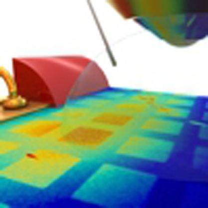 Point defects in diamond in the form of nitrogen vacancy centres are believed to be promising candidates for qubits in quantum computers. Grotz et al. present a method for manipulating the charge state of nitrogen vacancies using an electrolytic gate electrode.
The nitrogen-vacancy (NV) centre in diamond has drawn considerable interest over the past years in such diverse fields like quantum information processing1,2,3,4, single-spin magnetometry5,6 and plasmonics7,8. Most of these applications exploit the fact that the spin state of the negatively charged NV centre (NV−) can be initialized and read out optically. However, this state has been observed to become unstable, turning into the neutral charge state NV0 under various kinds of laser illumination9,10,11, close to the surface12,13,14,15 or at high implantation densities16,17. For the engineering18,19,20 of large-scale quantum processors3,21, it is therefore an outstanding goal to reliably control the charge state of an NV centre. This would not only enable stabilization of the NV− state but also allow to explore applications, which have been proposed for the neutral state22 NV0. In addition, inaccessible states23 such as NV+ could be explored, and a dynamic control of transitions between charge states might be established.
The charge state of defects in bulk semiconductors depends on the position of the Fermi level with respect to the defect's charge transition level, which is defined as the energy at which the defect takes up or loses an electron. For instance, the NV0/− level marks the transition from the neutral to the negatively charged state. Thus, when the Fermi level is shifted above a charge transition level, an electron is taken up by the defect and vice versa. For NV centres in diamond, the NV0/− charge transition level corresponds to the ground state of NV−, which is predicted to lie in the band gap 2.8 eV above the valence band maximum (VBM)23. The position of the NV+/0 level is expected to be below the NV0/− level. A static chemical control of the charge state of NV colour centres in diamond has recently been shown13,14,15. For instance, control of the Fermi energy was achieved by exploiting surface transfer doping in hydrogen (H)-terminated diamond24. In this case, atmospheric adsorbates on the surface provide acceptor states for electrons from the diamond, which shift the Fermi level below the VBM. This renders the H-terminated surface conductive due to a two-dimensional hole gas, which is formed in the potential well at the surface. Moreover, the Fermi level is shifted below the charge transition levels of shallowly implanted NV centres, which then ionize from NV− into NV0 and subsequently into a non-fluorescent state. We have previously shown that shallow implanted NV centres discharge below an oxygen (O)/hydrogen (H) patterned surface14.
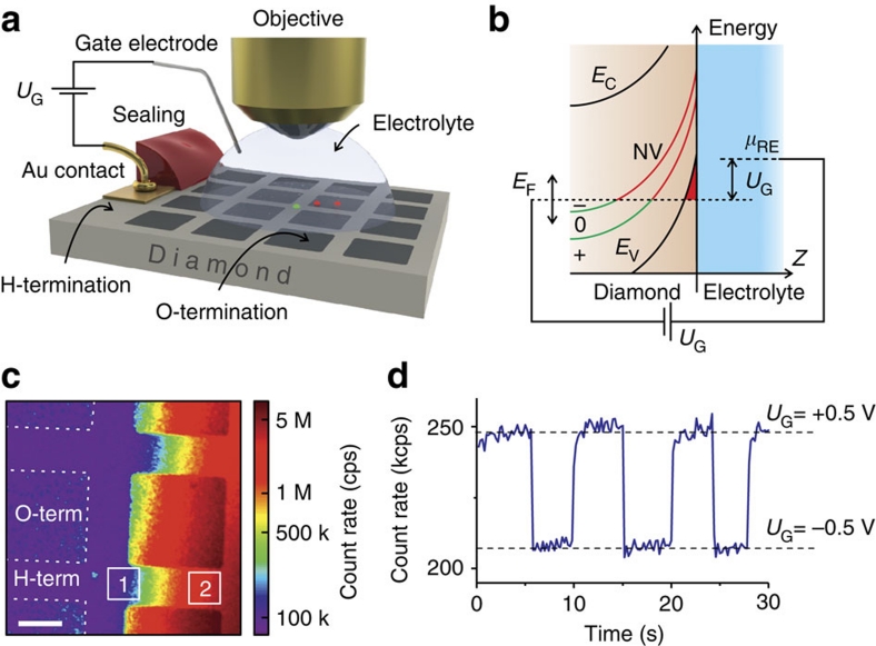
In this work, we demonstrate a method to dynamically manipulate the charge state of single NV centres with an electrolytic gate electrode. Similar to a diamond solution-gated field effect transistor25, an N+ implanted and subsequently H-terminated diamond is immersed into an electrolyte and a gate voltage UG is applied between a reference electrode in the electrolyte (potential μRE) and the diamond surface (Fig. 1a). This voltage allows to electrically shift the Fermi level at the diamond surface (Fig. 1b), which, at the same time, also changes its surface band bending. Upon varying the gate voltage, single centres can be switched from an unknown non-fluorescent state into the neutral charge state NV0, and the population of an ensemble of centres can be shifted from NV0 to NV−.
Figure 1. Electrical manipulation of the charge state of NV centres in diamond.
(a) Sketch of the experimental configuration showing the shallow-implanted NV centres in the O/H-patterned diamond surface. (b) Energy band schematic of the diamond/electrolyte interface. By applying a gate voltage between the gate electrode and H-terminated diamond, it is possible to control the Fermi energy level, moving it through the charge transition levels NV+/0 and NV0/−. (c) Fluorescence image of an O/H-patterned diamond with shallow-implanted NV centres under floating gate conditions. Regions 1 and 2 indicate areas with low and high dose of NVs, respectively. (d) Time trace of the fluorescence intensity upon changes between UG=±0.5 V (650 nm longpass filter) recorded on region (2).
Results
Electrical control of the charge state in NV ensembles
Experiments were conducted on electronic grade, synthetic, single-crystalline diamonds, with NV centres implanted at an average depth of 7 and 14 nm (5 and 10 keV implantation energy)26, where single optically resolved NV centres or densely implanted regions (regions 1 and 2 in Fig. 1c) could be examined. Samples were patterned with O- and H-terminated regions (see Fig. 1c). The conductive H-terminated surface was electrically contacted and the metal contacts isolated with silicone rubber. The sample was immersed in electrolyte, which was contacted by a platinum electrode.
We investigated the effect of the gate voltage on the fluorescence in densely implanted H-terminated regions (nitrogen implantation dose around 1013 cm−2) of the diamond surface (region 2 in Fig. 1c). Figure 1d shows the fluorescence count rate in this region, recorded with a NV−—selective 650 nm longpass filter while the gate voltage is switched between +0.5 and −0.5 V. The NV fluorescence intensity decreases by about 20% during this change and is fully recovered when switching back to +0.5 V (see Fig. 1d), suggesting that NV− centres are repeatedly discharged into NV0 or potentially NV+.
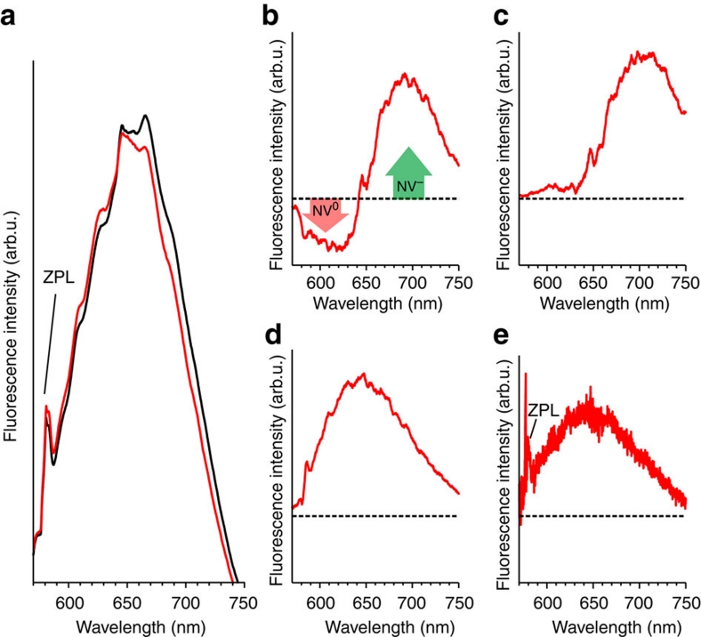
This is confirmed by optical spectra taken at both gate voltages (Fig. 2a). These spectra exhibit the characteristic emission of NV0 (with a zero-phonon-line at 575 nm) and NV− (zero-phonon-line at 637 nm), and therefore allow to infer the populations of the NV0 and NV− charge states.
Figure 2. Gate-dependent spectral properties of NV centres.
(a) Spectra of the H-terminated area of a 10 keV implantation in a region with high implantation density (black: UG=+0.5 V, red: UG=−0.5 V). ZPL, zero-phonon-line. (b–d) Difference of the spectra at UG=+0.5 V and UG=−0.5 V ((b) at ∼1013 cm−2, (c) at ∼1012 cm−2 and (d) at ∼1011 cm−2). The dashed line indicates zero level. (e) Difference spectrum of a single NV centre (implantation density ∼1011 cm−2) when switching from UG=+0.4 V to UG=−0.4 V. The dashed line indicates zero level.
The resulting change in the spectrum upon varying voltage is more clearly visible in Fig. 2b, which shows the difference between the spectra of Fig. 2a. Starting from a mixed population of negatively, neutrally and, potentially, positively charged NV centres, the amount of NV− increases at the expense of NV0 when the gate voltage changes from −0.5 to +0.5 V. We tentatively interpret the relatively small decrease of the NV0 fluorescence by assuming that simultaneously to the NV0 to NV− conversion, new NV0 centres are created from non-fluorescent positively charged NV+ centres.
As previously reported for H-terminated diamond surfaces in contact with air14, the relative population of charge states of the NV centres depends on the implantation dose and is shifted to more negative charge states for increasing dose. This is illustrated in Fig. 2b–d, which present difference spectra at varying implantation doses. In regions of high implantation dose (∼1013 cm−2, Fig. 2b), most NVs are in the negatively charged NV− state, with few NVs being neutrally charged. A change of the gate voltage shifts this distribution and induces an increase of NV− fluorescence at the expense of the NV0 component. In regions of low implantation dose (approximately 1011 cm−2, Fig. 2d), the NV− state is not populated at all and only few centres are in the neutral state NV0, whereas most centres discharge into a non-fluorescent state, potentially NV+. Changing the gate voltage shifts this equilibrium between NV0 and NV+. In the spectra, this manifests itself as a rise of the NV0 component, probably at the expense of an invisible NV+ component. For medium implantation dose (approximately 1012 cm−2, Fig. 2c), the spectrum is an interpolation between Fig. 2b, d. We observe a rise of the NV− component, which is not accompanied by a decrease in the NV0 component. We tentatively attribute this latter observation to the NV0 population being simultaneously replenished from an invisible NV+ population.
Switching behaviour of individual NV centres
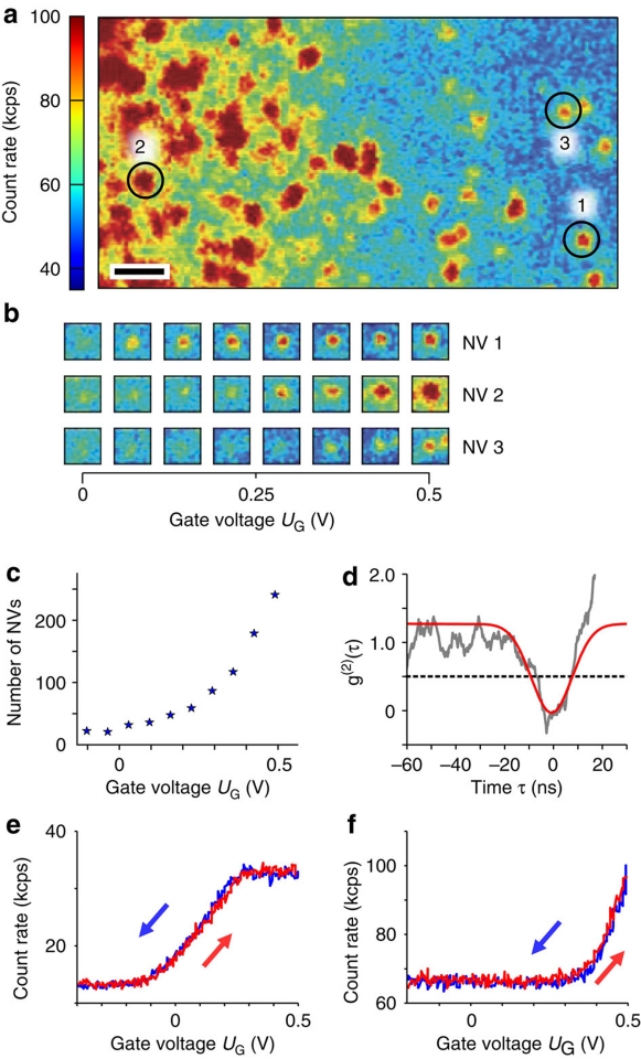
We were able to demonstrate electrical control of the charge state not only of an ensemble of NV centres, but even on a single-centre level in a sparsely implanted region (Fig. 3a, nitrogen implantation dose ∼1010 cm−2, similar to region (1) in Fig. 1c). As shown in Fig. 2e, centres exhibit the characteristic spectrum of NV0.
Figure 3. Charge state control of single NV centres.
(a) Fluorescence image of a 5 keV spot in a hydrogenated region at gate potential UG=0.5 V, bar indicates 1 μm. (b) Selected centres at various gate voltages. (c) Number of NV centres visible in the scanned region of (a) at different gate voltages. (d) Photon statistics g(2)(τ) measured on a single centre (background corrected, UG=0.5 V). (e,f) Gate-voltage dependence of the fluorescence intensity of two single NV centres.
Upon increasing the gate voltage towards more positive values, an increasing number of NV centres become visible (Fig. 3b, c), most of which are single centres as confirmed by measuring photon statistics g(2)(τ) (Fig. 3d). To study the switching process of a single centre in more detail, we monitored the fluorescence intensity of several single centres as a function of the applied gate voltage (Fig. 3e, f). Fluorescence sets in above a certain threshold voltage and grows for increasingly positive voltages, as the centre is transferred from a non-fluorescent state, possibly NV+, into the fluorescent state NV0. We observed that the exact value of the threshold voltage differs among the centres (Fig. 3e, f).
Discussion
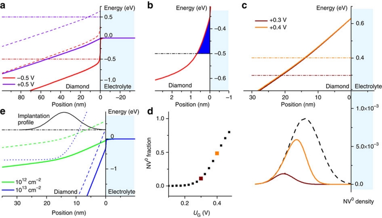
As we have discussed elsewhere14, the charge state of NV centres can be described in terms of the position of the charge transition level with respect to the Fermi level (EF). In our experiments, the applied gate voltage controls EF at the diamond surface (Fig. 1b). As a result, a band bending is imposed, so that the energy difference between charge transition level and Fermi level for a given centre depends on its distance to the surface. We numerically modelled this effect and calculated the band structure of diamond in contact with an electrolyte and, based on it, the charge state of the NV centres as described previously14 (see Methods section). A voltage UG can be applied between the diamond substrate and an external reference electrode in the electrolyte. Figure 4a illustrates the resulting energy band structure of H-terminated diamond in contact with an electrolyte for two different voltages: UG=±0.5 V. The charge transition level of NV+/0 is set to 0.65 eV above the VBM to best fit the experimental results. This is in the region of the respective energy level reported in literature23,27. The energies are plotted such that the potential in the electrolyte is zero. For UG=−0.5 V, the simulations reproduce the two-dimensional hole gas at the diamond surface (blue area in Fig. 4b), where the Fermi level has been pushed below the VBM. As the charge transition level follows the VBM with a constant energy distance, it will intersect with the Fermi level only deeper in the diamond. This marks the position where an NV centre will change its charge state upon a small variation of the applied voltage UG (see Fig. 1b). The closer the NV centre to the surface, the more positive gate voltage is required to change its charge state from NV+ to NV0. The varying threshold voltages observed for different NV centres (Fig. 3e, f) can therefore be interpreted as a result of the different distances of the NV centres to the surface or different local environments. An NV centre implanted deep in the diamond crystal would show a charging from NV+ to NV0 (onset of fluorescence) at more negative gate voltages, compared with a shallow centre. Figure 4c shows a detail of the energy band structure for two different gate voltages, 0.3 and 0.4 V, illustrating the intersection between EF and the charge transition NV+/0. In addition, the implantation profile is compared with the density profile of NV0 at these two gate voltages, indicating that the NV0 charge state can only exist in those regions where the Fermi level is above the charge transition level NV+/0. Integrating the density profile of NV0 for different applied potentials and comparing it to the total number of implanted NV (Fig. 4d), the calculated NV0 fraction nicely reproduces the experimental gate dependence shown in Fig. 3c.
Figure 4. Simulation of the energy band structure of H-terminated diamond in contact with an electrolyte.
(a) At UG=−0.5 V (red), the Fermi level EF (dash-dotted line) crosses the charge transition level NV+/0 (dashed line) much deeper in the diamond as compared with UG=+0.5 V (blue). (b) At negative UG, the Fermi level lies below the VBM (solid line) in the surface region, inducing a two-dimensional hole gas (2-DHG; blue area). (c) Energy band schematic showing the intersection of the Fermi level with the NV+/0 level at UG=0.3 V and UG=0.4 V. The density profile of neutrally charged NV is shown in comparison with the implantation. (d) Simulated fraction of neutrally charged NV versus the gate voltage. (e) VBM and the NV+/0 (dashed lines), as well as the NV0/− charge transition levels (dotted line), are shown for two different implantation dose (1012 and 1013 cm−2). The background nitrogen concentration is 50 p.p.b. The implantation density profile for 10 keV is shown for reference.
In principle, application of an even higher gate voltage should allow to raise the Fermi level even above the NV0/− level, and hence charge these single centres into the NV− state. We were not able to demonstrate this experimentally, as the range of accessible gate voltage is limited by the risk of surface oxidation.
However, the NV0/− level could be reached in regions of higher implantation dose. The key idea can be understood from Fig. 4e. The strength of the band bending in the diamond depends on the density of impurities, which can be varied by the dose of implanted nitrogen. At a fixed depth, a stronger band bending lowers all energy levels with respect to the Fermi level and is therefore indistinguishable from an increase of the gate voltage. Thus, a lower gate voltage allows to shift the Fermi level across the NV0/− level.
Figure 4e illustrates this effect for two cases of low and high implantation dose. An implantation dose of 1012 cm−2 induces a weaker band bending. Here, centres very close to the surface (see implantation profile in Fig. 4e) remain in their positive charge state. The rest of the implanted centres will be neutrally charged as EF is above the NV+/0 level. For a higher implantation dose of 1013 cm−2, the band bending within the first 20 nm is strongly enhanced because of the additional nitrogen donors implanted close to the surface. Therefore, no NV centres will be positively charged and some (up to a depth of around 10 nm) will be in the neutral state. At this depth, the Fermi level rises even above the NV0/− charge transition level, so that all deeper centres will be negatively charged.
It is by means of this effect that we were able to demonstrate switching between NV0 and NV− in Fig. 2b. By performing the experiment at high implantation dose (∼1013 cm−2), we place ourselves in the 'blue' scenario of Fig. 4e. The strong band bending associated to this high implantation dose implies that most NV centres remain negatively or neutrally charged. Here, a change of UG from −0.5 to 0.5 V increases the NV− fluorescence at the expense of the NV0 component as seen in Fig. 2b.
As the dose is lowered (Fig. 2d, e), we place ourselves in the 'green' scenario of Fig. 4e where the band bending is weak. Under these conditions, only the NV+/0 level intersects with EF within the implantation region, and a shift of the gate voltage mainly causes the conversion between NV0 and NV+. As the NV−/0 level is situated higher above the valence band, the crossing between EF and this charge transition level is expected further away from the diamond surface where no NV centres are implanted. Thus, a much larger gate voltage would be necessary to shift this crossing close to the implantation region in the vicinity of the surface. Because of the risk of surface oxidation, this is experimentally not accessible, so that single negatively charged NV centres cannot be observed in our present setting.
In conclusion, we have shown that an electrical manipulation of the charge state of shallow implanted NV centres below hydrogenated diamond surfaces is possible by using an external gate electrode. Ensembles of NV centres can be switched reversibly between NV0 and NV− by the gate voltage, whereas the charge state of single NV centres can be switched between positive and neutral. Numerical simulations, modelling the effect of the gate electrode on the diamond band structure, provide a quantitative description of the experimental results. These findings offer a first way to reversibly control the charge state of the NV centres in an extremely versatile manner, providing an important tool for the use of single NV centres for diamond-based spintronics or sensing applications. Furthermore, our results open the way to study formerly unstable or unknown charge states like NV0 and the positively charged NV+, for which several applications have already been proposed22.
Methods
Sample preparation
Experiments were conducted on electronic grade, synthetic, single-crystalline diamonds with a nitrogen concentration specified below 5 p.p.b. (purchased from Element Six Ltd). Two samples were used with NV centres created by the implantation of 15N+ ions with an energy of 5 and 10 keV per ion, respectively, at an implantation angle of 0°, followed by thermal annealing at 800 °C29. The average implantation depths can be estimated by SRIM calculations26 to be 7 and 14 nm. The ion beam was defocused to vary the implantation dose over three orders of magnitude (1010–1013 ions per cm2). This allows experiments on either single optically resolved NV centres or on densely implanted regions (regions 1 and 2 in Fig. 1c). Samples were patterned with oxygen (O)- and hydrogen (H)-terminated regions (see Fig. 1c) by photolithography and plasma treatment in a microwave-assisted plasma reactor. The O-terminated regions serve as reference areas to determine the local implantation density.
The H-terminated surface was electrically contacted and isolated with a chemically stable silicone rubber. A potassium phosphate buffer (10 mM K-PBS buffer, 50 mM KCl, pH7) was used as a gate electrolyte and immersion liquid, and showed no fluorescence upon laser excitation. The electrolyte was contacted with a Pt electrode, and gate voltages from 0.5 to −0.5 V were applied between the diamond surface and the electrode. No voltages outside this potential window were applied to avoid electrochemical oxidation of the surface.
Experimental setup
Optical measurements were performed with a home-built confocal microscope. A continuous-wave, diode-pumped, frequency-doubled Nd:YAG laser at a wavelength of λ=532 nm was used to excite the NV centres. The fluorescence signal was filtered by a 650-nm longpass filter and recorded by an avalanche photodiode or, alternatively, filtered by a 560-nm longpass filter and routed to a spectrometer (Acton 2300, Princeton Instruments with Pixis 100B camera).
Modelling and numerical simulations
The model for numerical simulations of the experimental results is based on the assumption that the NV centre exists in one of three charge states: negative (NV−), neutral (NV0) and positive (NV+). We assume that photoexcitation of these centres into highly excited states near the conduction band leads to rapid thermalization. The charge state is then determined exclusively by the relative position of the Fermi level with respect to the charge transition levels. The fluorescence intensity of NV− and NV0 is a measure of the ground state occupation of these charge states. In this way, we reduce the complex multi-level system of all ground, excited and metastable states of all defects in the diamond to an effective three-level system of NV charge transition states23, whose equilibrium occupation is governed exclusively by the position of the Fermi level.
By assuming thermal equilibrium, we neglect that photoexcitation could lead to a non-equilibrium distribution. In particular, traps above the Fermi level could be populated upon laser excitation. However, these traps are likely to thermalize with their local environment on a fast timescale. We consider this effect to be small and therefore use the thermal equilibrium model in which the population of states is exclusively governed by the position of the Fermi level. Although the assumption of thermal equilibrium is a nontrivial approximation, we have so far not seen a departure from this model, neither in the results of this work nor in previous results14.
Numerical simulations were performed using the nextnano software3. Nextnano is a semiconductor device simulation tool developed at the Walter Schottky Institute to predict and understand a wide range of electronic and optical properties of semiconductor structures and nanostructures30. It can calculate the electronic band structure, the carrier density and the electrostatic potential of a one-, two- or three-dimensional device consisting of different materials in a self-consistent manner. A detailed description of the nextnano simulation techniques has been published29.
The single band effective mass Schrödinger equation is coupled to the Poisson equation via the charge density as described by the wave functions in the diamond, which then is solved numerically in a self-consistent manner. The occupation of the subbands and defect levels in the band gap is determined by the energetic position relative to the Fermi level. The diamond is modelled in contact with an electrolyte and a gate voltage UG is applied between the diamond and an external reference electrode in the electrolyte. We use the Dirichlet boundary condition for the electrostatic potential in the bulk electrolyte and the Neumann boundary condition (vanishing electric field) deep in the diamond. The parameters used in the nextnano simulation are listed in Table 1.
Table 1. Parameters used in the nextnano simulation.
| Temperature | 298.15 K | |
| Diamond size | 3150 nm | |
| Conduction band energies, diamond | 7.35, 5.47, 5.47 eV | |
| VBM | 2.12 | (m0), hh |
| 0.70 | (m0), lh | |
| 1.06 | (m0), so | |
| Dielectric constant | 5.68 | |
| Doping: nitrogen (bulk) | 50 p.p.b.* | |
| Ionization energy, nitrogen | 1.7 eV30 | |
| Ionization energy, NV− | 2.58 eV | |
| Electrolyte | 10 mM K-PBS buffer, 50 mM KCl, pH7 | |
| Electrolyte size | 150 nm | |
| Grid size |
Down to 0.1 nm at the diamond/electrolyte interface |
|
*The higher nitrogen impurity level used in the simulations accounts for additional defects present in the diamond lattice.
Author contributions
B. G., M. V. H. and F. R. did the experiments; M. V. H., M. D. and J. G. performed the numerical simulations; B. N., S. P. and J. M. implanted the samples; F. J., J. W., M. S., F. R. and J. A. G. designed and coordinated the experiments; and B. G., M. V. H., F. R. and J. A. G. wrote the paper. All authors discussed the results, analysed the data and commented on the manuscript.
Additional information
How to cite this article: Grotz, B. et al. Charge-state manipulation of qubits in diamond. Nat. Commun. 3:729 doi: 10.1038/ncomms1729 (2012).
Acknowledgments
We thank Stefan Birner from the Walter Schottky Institute and Adam Gali from the Budapest University of Technology and Economics for fruitful discussions. We gratefully acknowledge financial support from the Baden-Württemberg Stiftung (Methoden für die Lebenswissenschaften), the DFG (FOR 1482, Quantum computing in isotopically engineered diamond, and FOR1493, Diamond Materials for Quantum Application), the Max-Planck-Society, the European Union (DINAMO and STREP DIAMANT), the Nanosystems Initiative Munich (NIM) and the Graduate School for Complex Interfaces of the Technische Universität München (CompInt).
References
- Jelezko F. et al. Observation of coherent oscillations in a single electron spin. Phys. Rev. Lett. 92, 076401 (2004). [DOI] [PubMed] [Google Scholar]
- Balasubramanian G. et al. Ultralong spin coherence time in isotopically engineered diamond. Nat. Mater. 8, 383–387 (2009). [DOI] [PubMed] [Google Scholar]
- Neumann P. et al. Quantum register based on coupled electron spins in a room-temperature solid. Nat. Phys. 6, 249–253 (2010). [Google Scholar]
- Neumann P. et al. Single-shot readout of a single nuclear spin. Science 329, 542–544 (2010). [DOI] [PubMed] [Google Scholar]
- Maze J. R. et al. Nanoscale magnetic sensing with an individual electronic spin in diamond. Nature 455, 644–647 (2008). [DOI] [PubMed] [Google Scholar]
- Balasubramanian G. et al. Nanoscale imaging magnetometry with diamond spins under ambient conditions. Nature 455, 648–651 (2008). [DOI] [PubMed] [Google Scholar]
- Kolesov R. et al. Wave-particle duality of single surface plasmon polaritons. Nat. Phys. 5, 470–474 (2009). [Google Scholar]
- Schietinger S. et al. Plasmon-enhanced single photon emission from a nanoassembled metal-diamond hybrid structure at room temperature. Nano Lett. 9, 1694–1698 (2009). [DOI] [PubMed] [Google Scholar]
- Gaebel T. et al. Photochromism in single nitrogen-vacancy defect in diamond. Appl. Phys. B-Lasers O 82, 243–246 (2006). [Google Scholar]
- Manson N. B. & Harrison J. P. Photo-ionization of the nitrogen-vacancy center in diamond. Diam. Relat. Mater. 14, 1705–1710 (2005). [Google Scholar]
- Waldherr G. et al. Dark states of single nitrogen-vacancy centers in diamond unraveled by single shot NMR. Phys. Rev. Lett. 106, 157601 (2011). [DOI] [PubMed] [Google Scholar]
- Santori C. et al. Vertical distribution of nitrogen-vacancy centers in diamond formed by ion implantation and annealing. Phys. Rev. B 79, 125313 (2009). [Google Scholar]
- Fu K. M. C. et al. Conversion of neutral nitrogen-vacancy centers to negatively charged nitrogen-vacancy centers through selective oxidation. Appl. Phys. Lett. 96, 121907 (2010). [Google Scholar]
- Hauf M. V. et al. Chemical control of the charge state of nitrogen-vacancy centers in diamond. Phys. Rev. B 83, 081304(R) (2011). [Google Scholar]
- Rondin L. et al. Surface-induced charge state conversion of nitrogen-vacancy defects in nanodiamonds. Phys. Rev. B 82, 115449 (2010). [Google Scholar]
- Martin J. et al. Confocal microscopy of color center distributions in diamond. J. Lumin. 83–84, 493–497 (1999). [Google Scholar]
- Mita Y. Change of absorption spectra in type-Ib diamond with heavy neutron irradiation. Phys. Rev. B 53, 11360–11364 (1996). [DOI] [PubMed] [Google Scholar]
- Pezzagna S. et al. Nanoscale engineering and optical addressing of single spins in diamond. Small 6, 2117–2121 (2010). [DOI] [PubMed] [Google Scholar]
- Schnitzler W. et al. Deterministic ultracold ion source targeting the heisenberg limit. Phys. Rev. Lett. 102, 070501 (2009). [DOI] [PubMed] [Google Scholar]
- Pezzagna S. et al. Creation and nature of optical centres in diamond for single-photon emission-overview and critical remarks. New J. Phys. 13, 035024 (2011). [Google Scholar]
- Toyli D. M. et al. Chip-scale nanofabrication of single spins and spin arrays in diamond. Nano Lett. 10, 3168–3172 (2010). [DOI] [PubMed] [Google Scholar]
- Gali A. Theory of the neutral nitrogen-vacancy center in diamond and its application to the realization of a qubit. Phys. Rev. B 79, 235210 (2009). [Google Scholar]
- Weber J. R. et al. Quantum computing with defects. Proc. Natl Acad. Sci. USA 107, 8513–8518 (2010). [DOI] [PMC free article] [PubMed] [Google Scholar]
- Maier F. et al. Origin of surface conductivity in diamond. Phys. Rev. Lett. 85, 3472–3475 (2000). [DOI] [PubMed] [Google Scholar]
- Dankerl M. et al. Hydrophobic interaction and charge accumulation at the diamond-electrolyte interface. Phys. Rev. Lett. 106, 196103 (2011). [DOI] [PubMed] [Google Scholar]
- Ziegler J. F. et al. SRIM - the stopping and range of ions in matter (2010). Nucl. Instrum. Meth. B 268, 1818–1823 (2010). [Google Scholar]
- Meijer J. et al. Generation of single color centers by focused nitrogen implantation. Appl. Phys. Lett. 87, 261909 (2005). [Google Scholar]
- Birner S. et al. nextnano: General purpose 3-D simulations. IEEE T. Electron Dev. 54, 2137–2142 (2007). [Google Scholar]
- Trellakis A. et al. The 3D nanometer device project nextnano: Concepts, methods, results. J. Comput. Electronics 5, 285–289 (2006). [Google Scholar]
- Farrer R. G. On substitutional nitrogen donor in diamond. Solid State Commun. 7, 685–688 (1969). [Google Scholar]


