Abstract
Prominent deflections are shown to occur in freestanding silicon nitride thin membranes when exposed to a 50 keV gallium focused ion beam for ion doses between 1014 and 1017 ions/cm2. Atomic force microscope topographs were used to quantify elevations on the irradiated side and corresponding depressions of comparable magnitude on the back side, thus indicating that what at first appeared to be protrusions are actually the result of membrane deflections. The shape in high-stress silicon nitride is remarkably flattopped and differs from that in low-stress silicon nitride. Ion beam induced biaxial compressive stress generation, which is a known deformation mechanism for other amorphous materials at higher ion energies, is hypothesized to be the origin of the deflection. A continuum mechanical model based on this assumption convincingly reproduces the profiles for both low-stress and high-stress membranes and provides a family of unusual shapes that can be created by deflection of freestanding thin films under beam irradiation.
INTRODUCTION
Ion beams are widely used for high-precision micro- and nanomachining and for imaging, surface modification, and analysis. It has been widely recognized that ion beams often induce compositional and morphological changes on solid surfaces due to atomic displacement, structural damage, sputter erosion, hydrocarbon contamination, and ion implantation.1-6 While such effects may in some situations be detrimental, they may also be exploited to create or tailor nanostructures. For example, the increased etch resistance of silicon caused by Ga+ doping has been exploited to generate etch masks for anisotropic etching,5 and Ar+ ion beams have been used to sculpt nanopores and other fine nanostructures in thin silicon nitride membranes.6 In the latter case, the relative roles of the ion beam in creating and annihilating surface point defects and in creating and relieving thin film stress remain poorly understood. As feature dimensions are reduced down to the nanometer scale, it becomes increasingly important to understand the effects of ion beams for fully exploiting material-related opportunities as well as understanding factors that may limit delicate nanostructure processing.
Freestanding thin films have been adopted as a platform for analytical micro/nanodevices.7,8 Silicon nitride is the most widely used material for such devices, because of its excellent electrical and mechanical properties. But the physics of ion beam-solid interaction has been limited primarily to bulk materials. Here we examined how localized ion irradiation affects freestanding membranes. We observed large deflections that occur in freestanding silicon nitride membranes when exposed to a gallium focused ion beam (FIB). The evolution of the membrane deflection was quantified using an atomic force microscope (AFM). We propose that ion irradiation generates biaxial compressive stress in silicon nitride, as it is known to do in other amorphous materials at higher ion energies.2,3,9-18 An analysis of the resulting mechanics provides good agreement with experimentally measured deflection profiles, as well as an explanation for the qualitatively different shapes observed in low-stress and high-stress silicon nitrides.
EXPERIMENT
Starting with (100) oriented silicon wafers coated on both sides with silicon nitride on top of a 500 nm thick thermally grown silicon dioxide (Silicon Quest International, Santa Clara, CA), photoresist was spin coated on both sides of the wafer. The photoresist on the back side of the wafers was patterned with square windows by exposing it to UV light. The pattern was transferred to the silicon nitride using reactive ion etching (RIE), and the exposed silicon dioxide was subsequently etched in a buffered oxide etch (six parts 40% NH4F and one part 49% HF). The remaining photoresist was stripped with acetone and the silicon was etched in a KOH solution (45% by weight in water) at 90 °C creating freestanding silicon nitride membranes. Any silicon dioxide remaining on the silicon nitride after the KOH etch was removed in a buffered oxide etch. Two types of silicon nitride were used: a stoichiometric silicon nitride with a large residual stress and a Si-rich nitride with reduced stress. Both were deposited using a low-pressure chemical vapor deposition (LPCVD) process. The properties and dimensions of both types of membranes are listed in Table I.
TABLE I.
Properties of the LPCVD silicon nitride membranes.
| High-stress SiNx | Low-stress SiNx | |
|---|---|---|
| Ea (GPa) | 222 | 222 |
| νa | 0.28 | 0.28 |
| σo (MPa) | 1000 | 180 |
| to (nm) | 200 | 500 |
| L (μm) | 67.5 | 100 |
Reference 26.
Freestanding silicon nitride membranes were irradiated with a FIB of 50 keV Ga+ and a beam current of 4 pA.19 The ion beam was generated in a Micrion 9500 HT system (currently serviced by FEI, Hilsboro, OR). The beam current was measured directly using a Faraday cup with a picoammeter and calibrated before each experiment; the current was generally stable and reproducible throughout the experiments. The ion beam was focused in an area away from the target site to avoid implanting any ions in the target site and its immediate vicinity during this procedure. The focused ion beam was then moved to the target site and scanned over a predefined pattern using the digital patterning mode with a pixel spacing of 10 nm, a dwell time of 5 μs, and a retrace time of 5 μs. This scan was repeated until the specified dose was reached. The irradiation dose varied over three orders of magnitude between 1014 and 1017 ions/cm2. The lower doses, 1014–1015 ions/cm2, are equivalent to doses commonly used for imaging specimens with a scanning ion microscope. Simple structures such as squares, circles, and lines were written on the silicon nitride membranes with various doses. The electron flood gun, which is used to minimize charging of dielectric samples in imaging mode, was not used in the patterning mode. Charging of the membranes during implantation should have a minimal effect on the implanted dose, because the maximum potential difference built up across the membranes is limited by the breakdown field of the silicon nitride and is only a small fraction of the accelerating voltage of the ions. After ion implantation, the surfaces were examined with an AFM. The AFM was operated in tapping mode to analyze the topography of the implanted areas. The AFM scans were performed at least 24 h after the FIB experiment to allow any FIB-induced charges to dissipate. Without delays of a few hours, these charges interfered with the AFM imaging, resulting in false topographic information. The radius of curvature of the AFM tip was on the order of 5 nm, i.e., approximately four orders of magnitude smaller than the typical radii of curvature observed in the experimental profiles.
RESULTS
Irradiation of a freestanding silicon nitride membrane with a focused gallium ion beam resulted in striking topographic changes of the membrane. In Fig. 1, we show AFM topographs of square structures with dimensions of 4 × 4 μm2 irradiated under uniform rastering to various doses. Irradiating the freestanding membrane with doses between 1014 and 1016 ions/cm2 resulted in prominent elevations ranging from 25 to 35 nm in height. No such elevations were seen upon irradiating supported areas of the same silicon nitride membrane (Fig. 2), although as expected irradiation of these supported membrane areas at doses in excess of 5 × 10¹⁶ ions/cm2 resulted in material removal by sputter erosion. As will become evident (see below), the elevations in the freestanding nitride thin films were, in fact, due to out-of-plane deflections of the silicon nitride membranes, presumably the result of gallium ion implantation. This behavior should be contrasted with observations reported in the literature for the implantation of monolithic Si.20,21 When Si is irradiated with low doses of Ga+ ions, amorphization of the Si results in protrusions up to 2 nm in height. According to Fig. 2, any protrusions in substrate-supported silicon nitride are on the order of 1 nm or less in our experimental conditions. Such protrusions are caused by irradiation-induced strains and not amorphization, since the silicon nitride is amorphous as deposited.
FIG. 1.
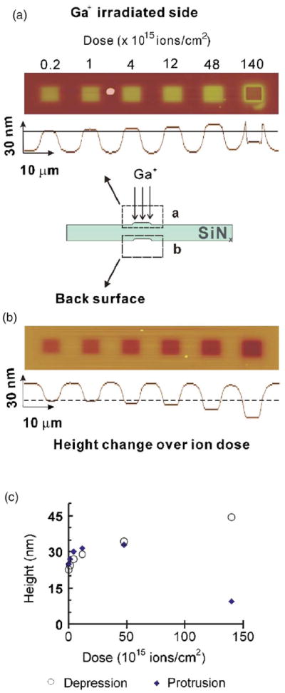
(Color online) AFM images and trace [(a) and (b)] and a schematic drawing (middle) of the deflection induced in a 25×25 μm2 freestanding high-stress SiNx membrane by a focused Ga+ ion beam. The AFM image and corresponding trace in (a) show the Ga+ irradiated side of the membrane; the AFM image and corresponding trace in (b) show the back side. The dose for each irradiated area is shown above the AFM images. The dashed lines through the trace profiles guide the eye to show how the elevations (top) and depressions (bottom) increase with ion dose. Material removal from the Ga+ irradiated side of the membrane masks the elevation in the area that received the highest dose (140×1015 ions/cm2). (c) Extent of the elevations and corresponding depressions of the silicon nitride membrane for increasing ion doses. The magnitude of the elevation decreases for the largest dose as the material is eroded in the irradiated area.
FIG. 2.
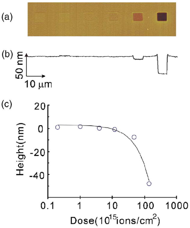
(Color online) (a) AFM image showing the change of surface topography of a supported high-stress silicon nitride film on a silicon substrate after FIB irradiation. The doses for each irradiation (from left to right) are 0.2, 1, 4, 12, 48, and 140×1015 ions/cm2. The surface profile (b) reveals that low doses induce a slight height increase, whereas larger doses, beyond approximately 5×10¹⁶ ions/cm2, produce net erosion in the irradiated area. (c) Step height as a function of irradiation dose.
AFM images (Fig. 1) revealed that the irradiated 4 × 4 μm2 areas of the freestanding membrane deformed uniformly toward the source of the beam, producing a flattopped protruding structure on the face of the membrane receiving the incident beam, and a similar flat-bottom depression on the opposite face, or back surface, of the membrane. No significant deformation occurred in regions outside of the irradiated shoulders that bordered the 4 × 4 μm2 irradiated areas. At and above doses of 140 × 1015 ions/cm2, a crater was formed in the rastered area but the shoulder structure just outside of the irradiated area remained.
To fully understand these morphological changes, both the elevations on the irradiated face as well as the corresponding depressions on the opposite face were measured with the AFM [Fig. 1(b)]. At doses below 15 × 1015 ions/cm2, the magnitude of the elevations and the depth of the corresponding depressions were comparable [Fig. 1(c)]. This made it clear that the elevations were indeed the result of membrane deflections.
A striking aspect of the membrane deflections we observed was the uniform flatness of the raised area on the surface of the silicon nitride membrane facing the ion beam and the corresponding depression on the back surface. The flatness of these surfaces was not a consequence of constraints imposed by the square patterns irradiated in Fig. 1, as other patterns of irradiation, including long strips and circular patterns of various diameters, produced similarly flat profiles. Thus, the entire ca. 15 μm diameter circular pattern irradiated in Fig. 3 formed a strikingly flattopped 33 nm elevation on the side of the film facing the ion beam and a corresponding flat bottomed depression of the same magnitude on the back side. Low-stress membranes, by contrast, showed a much more gradual deflection, as illustrated in Fig. 4.
FIG. 3.
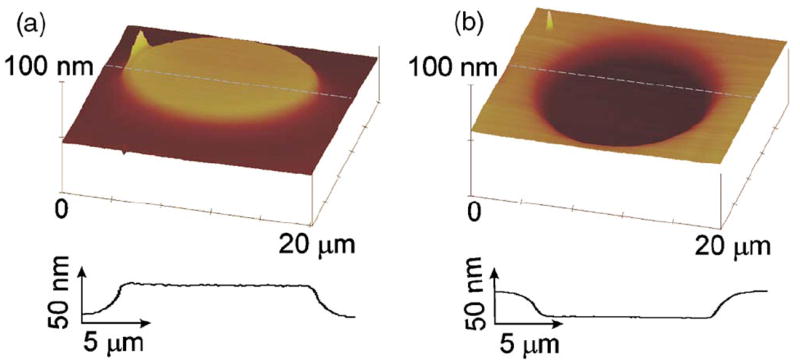
(Color online) AFM images showing the elevation (a) and corresponding depression (b) that are induced in a freestanding high-stress silicon nitride membrane by ion beam irradiation (1015 ions/cm2) in a circular pattern. The elevation occurred on the irradiated side and the corresponding depression on the back side of the freestanding membrane. AFM sectional profiles, shown below the corresponding AFM images, reveal the flat profiles. The magnitudes of the elevations and corresponding depressions are nearly equal.
FIG. 4.
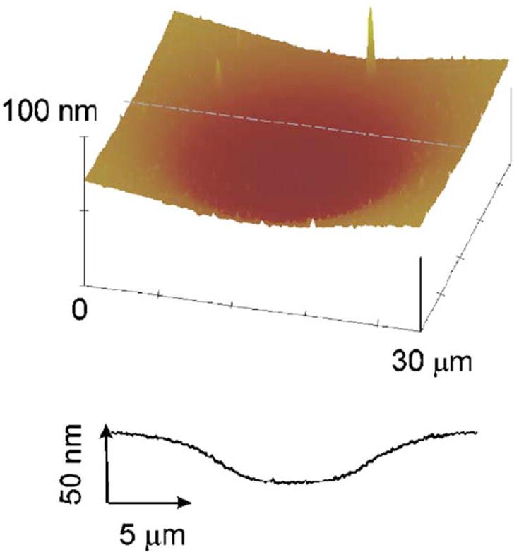
(Color online) AFM image showing the depression induced in a freestanding low-stress silicon nitride membrane by ion beam irradiation (625×1015 ions/cm2) over a circular region. The AFM scan was made on the back side of the membrane. The AFM sectional profile, shown below the AFM image, reveals the gradual deflection of the membrane.
A simple mechanical model for the membrane deflection
It has been known for many years that amorphous materials subjected to MeV ion irradiation develop biaxial plastic deformation by expanding in directions perpendicular to the ion beam at constant volume.9 The magnitude of the anisotropic deformation is known to scale with the electronic energy loss rather than with energy loss in nuclear collisions.10 Comprehensive studies in SiO2 have afforded a reasonably complete picture of the phenomenon.11-16 Electronic energy loss in the ion track creates a thermal spike accompanied by thermal expansion. Shear stresses relax when the innermost region of the ion track exceeds the “flow temperature;” subsequent thermal contraction during rapid quenching locks in an expansion perpendicular to the ion track. From extrapolating data taken at high energy, it appeared that anisotropic deformation does not occur below about 1 MeV.17,18 Recently, however, colloidal SiO2 particles have been shown to undergo anisotropic deformation at energies as low as 300 keV, with no threshold evident.2 Even at energies below this, where nuclear stopping predominates and ions undergo frequent elastic nuclear scattering, on average the ion track maintains some directionality and the mechanism described above may operate. Very little is known about the behavior of silicon nitride under ion irradiation, but the mechanical model presented below is built upon the assumption that silicon nitride tends to undergo biaxial expansion under 50 keV Ga+ ion irradiation over the depth of the implantation. In a confined region within a thin membrane supported along its perimeter by attachment to a substrate, this results in membrane deflection.
A simple mechanical model based upon this assumption makes quantitative predictions about the magnitude of the deflection and convincingly explains its origin. We assume that the silicon nitride has a residual biaxial tensile stress of magnitude σo in it. Implantation of Ga+ ions alters the stress state in the irradiated portion of the membrane causing the membrane to deflect. The mechanical effect of the implantation is most readily visualized, as shown schematically in Fig. 5. Before the implantation, the stress in the membrane is uniform through its thickness. In a thought experiment, we remove the section of the membrane that will be affected by the implantation [Fig. 5(b)]. To maintain the stress in this section, surface tractions σo need to be applied to the edges of the section; to maintain the stress in the membrane, tractions σo are also applied to the exposed edges of the membrane. As a result of the implantation process [Fig. 5(c)], the dimensions of the implanted region change [Fig. 5(d)] and the applied surface tractions need to be changed to σimp (Fig. 5(e)] before the section can be reinserted into the membrane [Fig. 5(f)]. From a mechanical point of view, the net effect of the implantation is then to apply a line force F to the edge of the implanted region of magnitude
| (1) |
where timp is the depth of the implant. This force acts in the center plane of the implanted section. It is convenient to replace the line force with a mechanically equivalent loading that consists of the same line force F acting along the center plane of the membrane [Fig. 5(g)] and a line bending moment
| (2) |
where to is the thickness of the membrane. According to the Barré de Saint–Venant’s principle,22 this equivalent loading produces the same membrane deflection as the actual stress state. The foregoing assumes that the stress in the implanted region is uniform. This need not be the case: if the stress after implantation is not uniform, σimp has the meaning of the average stress in the implanted region. A nonuniform stress may have a bending moment associated with it, which would have to be added to the bending moment defined in Eq. (2). This contribution is negligible if the implantation depth is small compared to the total membrane thickness. In the following, we assume that the deformation of the membrane is elastic—this is a good assumption provided that to≫timp. We further assume that the implant does not change the overall stress in the membrane outside the implanted region, i.e., we ignore the effect of F. This is valid if
| (3) |
where a is a characteristic size of the implanted region (e.g., width or radius), and L is the width of the membrane. Finally, we assume that the deflection of the membrane does not alter the in-plane membrane stresses significantly, i.e., the deflection is smaller than the membrane thickness.23 We now consider two cases depending on the shape of the implanted region: an infinitely long strip and a circular region.
FIG. 5.
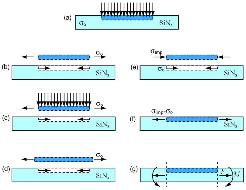
(Color online) Schematic illustration of the mechanical effect of an ion implant on a freestanding membrane. F and M form a mechanically equivalent loading system.
The plane-strain case
If the implanted region is an infinitely long strip of width 2a, the membrane deflection problem is reduced to one of the plane strains. We assume that the membrane has a width 2L. The equations describing the deflection of the membrane are then relatively simple and follow directly from the moment equilibrium,23 as shown in Fig. 6,
| (4) |
where D is the membrane bending stiffness given by
| (5) |
and where w1 and w2 are the deflections in the implanted region and elsewhere in the membrane, respectively. Mc is the bending moment imposed by the frame surrounding the membrane, and E and ν are Young’s modulus and Poisson’s ratio of the membrane material. The boundary conditions are as follows:
| (6) |
FIG. 6.

(Color online) Schematic illustration of the bending moments exerted on a section of the membrane. Note that the sign of the moments is defined conventionally as shown in the figure.
The conditions evaluated at L ensure that the membrane is clamped; the conditions at a enforce continuity of the membrane between the irradiated section and the remainder of the membrane; the condition at the origin enforces mirror symmetry. The five boundary conditions allow determination of the four integration constants that arise from integrating the differential equations in Eq. (4), as well as the unknown bending moment Mc. Solution of the differential equations is elementary but tedious and the membrane deflection in normalized form is given by
| (7) |
In these expressions, ω1 = w1σoto / Mimp, ω2 = w2σoto / Mimp, ξ = x/L, α=a/L, and
| (8) |
The dimensionless parameter β compares the resistance of the membrane to out-of-plane deflections as a result of its residual stress with the bending stiffness of the membrane. If β is large the membrane behaves as a taut membrane, if β is small it behaves more like a plate. The value of this parameter has a significant effect on the shape of the deflections, as illustrated in Fig. 7: large values of β result in membranes with most of the curvature centered around the edge of the implanted region and that are flat inside and outside the implanted region; small values of β produce membranes that are curved throughout the implanted region. In general, the characteristic length over which the curvature extends is given by
| (9) |
and the condition for a flat deflection profile can be more precisely expressed as
| (10) |
FIG. 7.
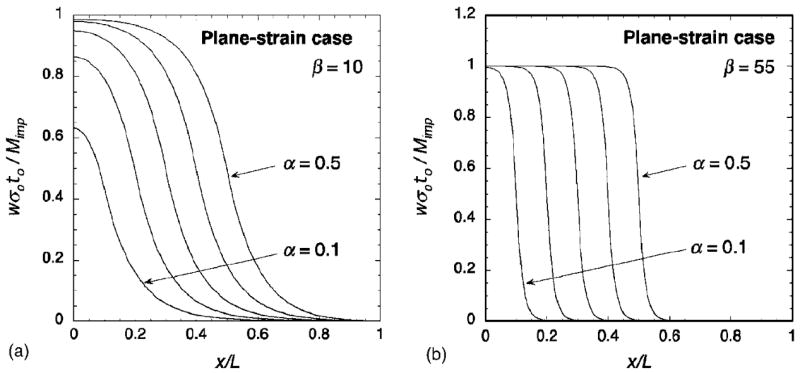
(Color online) Normalized membrane deflection as a result of ion implantation for the plane-strain case: (a) membrane with a small value of β; (b) membrane with a large β value. Deflections are shown for α increments of 0.1.
The axisymmetric case
Consider a circular membrane of radius L. The deflection of the membrane after a circular region of radius a is implanted is described by the following set of differential equations:23
| (11) |
with boundary conditions
| (12) |
The last boundary condition expresses that a line moment is applied to the edge of the implanted region, the other conditions are as before. This set of equations can be solved analytically, this time in terms of modified Bessel functions. Explicit expressions are too long to be given here, but can again be formulated in terms of the dimensionless parameters α and β. As shown in Fig. 8, the general shape of the deflections is very similar to that for the plane-strain case. The condition for a flat deflection profile is similar to Eq. (10).
FIG. 8.
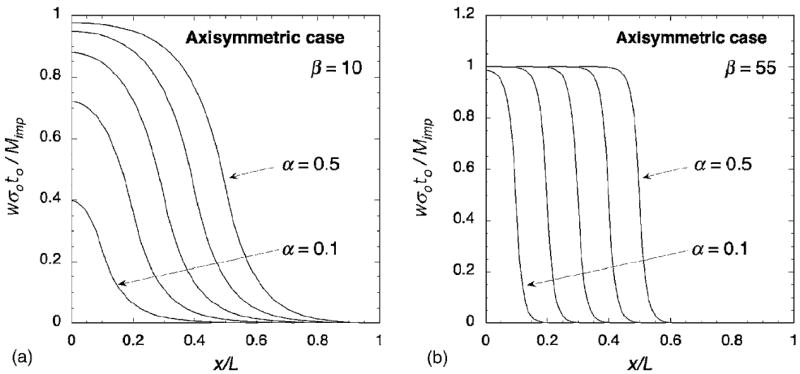
(Color online) Normalized deflection as a result of ion implantation in a circular region for an axisymmetric membrane with a small β value (a) and a large β value (b). Deflections are shown for α increments of 0.1.
DISCUSSION
Inspection of Eqs. (2), (7), and (8) along with the axisymmetric solutions shows that the deflection of the membrane caused by the ion implantation scales linearly with the stress change induced by the implant as well as with the implant depth. The deflection is also a function of the dimensionless parameters α and β, which depend on geometric parameters and on the mechanical properties of the membrane. Thus, if the values of α β, and the implant depth are known, the stress induced by the implant can be determined from the deflection of the membrane. The properties of the silicon nitride membranes used to calculate the value of β are listed in Table I for both high-stress and low-stress nitrides. The value of α follows directly from the size of the implanted area. The implant depth was assumed equal to the projected ion range plus three times the standard deviation,24 which was determined to be 54.6 nm by means of a SRIM simulation25 (SRIM-2003.26) based on an assumed silicon nitride density of 3.29 g/cm3. Figures 9 and 10 show the experimental deflections of a low-stress and a high-stress membrane for the case where circular regions were implanted with 25×1015 ions/cm2. Also shown are the analytical deflections based on the mechanical model described in the previous section with the implant stress as the sole fitting parameter. Agreement between the experimental results and the deflections obtained from the model is remarkably good. The model correctly predicts the shape of the deflection for both types of membranes. Similarly good agreement between experimental results and the plane-strain solutions is obtained for the case where the implanted area is rectangular in shape.
FIG. 9.
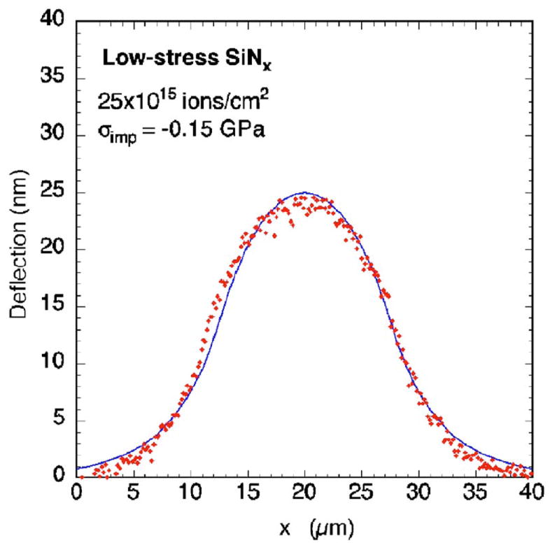
(Color online) Experimental deflection of a low-stress silicon nitride membrane for the case where a circular region with a 15 μm diameter was implanted with 25×1015 Ga+ ions/cm2. The solid line is the shape predicted by the model.
FIG. 10.
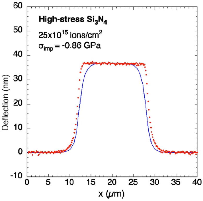
(Color online) Experimental deflection of a high-stress silicon nitride membrane for the case where a circular region with a 15 μm diameter was implanted with 25×1015 Ga+ ions/cm2. The solid line is the shape predicted by the model.
Despite the general good agreement between model and experimental results, there is a small discrepancy in the deflection at the edge of the implanted region of the high-stress membranes (Fig. 10). Because the predicted curvature just outside the implanted region agrees well with the experimental results, this discrepancy is most likely due to irradiation induced viscous flow in the implanted region. The implanted region in the high-stress membranes makes up a significant fraction of the total membrane thickness and any inelastic effects that take place in this layer will have an effect on the final shape of the membrane. Irradiation induced viscous flow has been characterized thoroughly for SiO2.11,14
The very flat profiles observed for the high-stress membranes present an alternate, much simpler avenue for determining the implantation-induced stress in membranes with a large β value. Because the deflection profile is flat inside and outside the irradiated regions, the bending moment in the membrane is also zero in those areas. For the plane-strain case, it is then straightforward to write a moment balance for a section of the membrane that crosses the boundary of the irradiated zone. Since cross sections of flat segments of the membrane do not have any resultant bending moment, it follows directly from Fig. 11 that
| (13) |
or with Eq. (2)
| (14) |
FIG. 11.
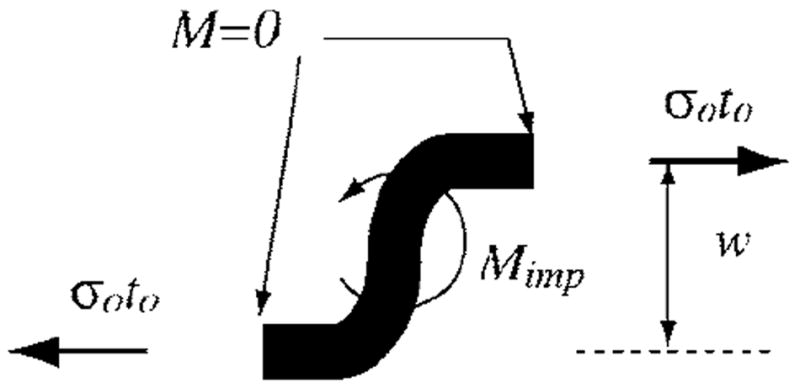
(Color online) Schematic illustration of the bending moments applied to a section of a membrane with a large β value. Cross sections of horizontal segments of the membrane do not have any resultant bending moment.
Equation (14) provides a direct relationship between the stress induced in the implanted region and the membrane deflection and is valid as long as the deflection profile has flat sections. It is straightforward to verify that the same equation also applies to the axisymmetric case. Equation (14) is independent of the precise shape of the membrane near the edge of the implanted region. Moreover, Eq. (14) can be used to determine the implantation stress without knowledge of the mechanical properties of the membrane, as long as the residual stress in the membrane is known. Because it is generally much easier to determine the residual stress in a thin film (e.g., by substrate curvature techniques) than to measure its Young’s modulus or Poisson’s ratio, membranes with large β values present a significant advantage over membranes with small β values for studying implant-induced stresses.
Figure 12 shows the stress induced by the ion implantation for the high-stress and low-stress membranes. Data from both circular and rectangular implanted regions are included. The results for the low-stress membranes were obtained by fitting the appropriate analytic expressions for the membrane deflections with the induced stress as sole fitting parameter. The stress values for the circular patterns on the high-stress membranes were calculated using both the fitting procedure and Eq. (14) with no appreciable difference between the results. The deflection analysis yields values for the implant-induced stress normalized by the residual stress in the membrane. Because the residual stress in the membranes was not measured independently, the normalized values are plotted in Fig. 12.
FIG. 12.
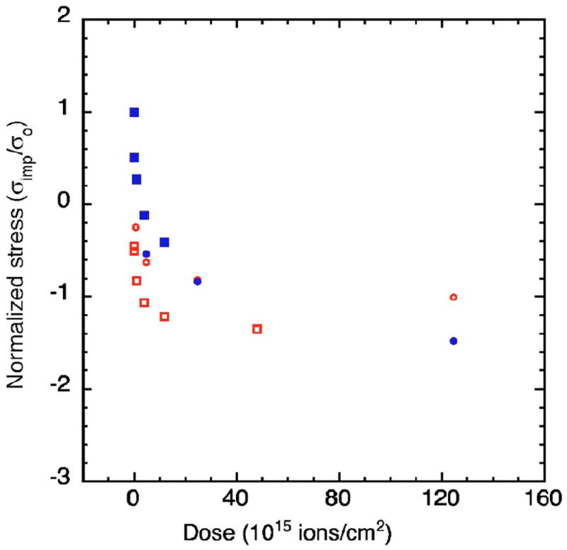
(Color online) Normalized ion-implantation-induced stress vs ion dose. The solid symbols represent the data for the low-stress nitride, whereas the open symbols represent the data for the high-stress nitride. The squares represent the results obtained from rectangular implanted areas, whereas the circles represent the results from circular areas.
As is evident from the figure, there is a systematic difference between the results obtained from circular and rectangular implant regions. Because these implants were performed on different wafers, the differences are most likely attributed to a difference in residual stress between the wafers. Moreover, the results obtained for the rectangular regions are sensitive to the precise values of the mechanical properties of the silicon nitride membrane because they do not quite satisfy Eq. (10), while those for the circular regions are not so sensitive. For both nitrides, the implant-induced stress decreases with increasing dose. Similar behavior has also been observed for LPCVD silicon nitride by Yamamoto et al.24 for B, P, As, and Ar at 50–350 keV. However, they focused on reducing the magnitude of the tensile stress and stopped at lower doses than most of those reported here. Had they continued implantation to higher doses, they may have observed the development of compressive stress.
The behavior of the normalized stress as a function of dose is similar for both types of nitride, but there is a significant difference if the absolute value of the implant-induced stress is considered. The final compressive stress in the low-stress membranes is much lower than in the high-stress membranes. The explanation for this observation is open at the moment. Differences in the interaction with ion beams for different types of silica have been observed as well,2 and have been conjectured to be the manifestation of different flow temperatures in the different silicas.15 A similar explanation for silicon nitride is tenable.
SUMMARY
Uniformly rastered FIB irradiation of a confined region in the center of a freestanding silicon nitride membrane, supported along its perimeter by attachment to a substrate, results in prominent out-of-plane membrane deflections. AFM topographs quantify both the front-side elevations and corresponding back-side depressions of comparable magnitude, indicating that the measured topography is the result of membrane deflection. In high-stress silicon nitride the topographic profiles exhibit clearly flattopped deflections for ion doses between 1014 and 1017 ions/cm2. In low-stress silicon nitride the deflections are similar in magnitude but more gradually sloped. The prominent deflection by ion beam irradiation is specific for freestanding membranes; no such deflections were observed when a silicon nitride film still attached to the substrate was irradiated under identical conditions. The height of deflection increases with ion dose in a nonlinear manner, with little or no further deflection at the doses beyond 50×1015 ions/cm2. Ion beam induced biaxial compressive stress generation, which is a known deformation mechanism for other amorphous materials at higher ion energies, is hypothesized to be the origin of the membrane deflection. A continuum mechanical model based on this assumption reproduces the profiles for both low-stress and high-stress membranes with the implant stress being the only free parameter. The predicted profile is determined by a dimensionless aspect ratio—the ratio of the width of the implanted region to that of the membrane, and a dimensionless material parameter—the ratio of resistance to deflection from membrane tautness to that from bending stiffness as defined in Eq. (8). The remarkable flattopped deflection profile observed for the high-stress nitride is predicted to occur for relatively large values of both of these ratios.
The effect of ion beam on freestanding membranes is striking, creating topographic changes an order of magnitude greater than those in films supported on substrates under otherwise identical conditions. This effect could limit the application of the FIB for the fabrication or modification of delicate features on freestanding thin films even at very low doses for some cases. On the other hand, the ability of a FIB to generate such a structure in a highly controllable way could develop into a very useful tool for micro- and nano-fabrication.
Acknowledgments
This research was supported by the National Institute of Health, Award Nos. R01 HG02338 and HG03703 [to three of the authors (Y.R.K., P.C., and D.B.)], and by the National Science Foundation, Award Nos. NSF-DMR-0133559 [to one of the authors (J.J.V.)] and NSF-DMR-0306997 [to another author (M.J.A.)].
Contributor Information
Y.-R. Kim, Department of Molecular and Cellular Biology, Harvard University, 7 Divinity Avenue, Cambridge, Massachusetts 02138.
P. Chen, Department of Molecular and Cellular Biology, Harvard University, 7 Divinity Avenue, Cambridge, Massachusetts 02138.
M. J. Aziz, Division of Engineering and Applied Sciences, Harvard University, 29 Oxford Avenue, Cambridge, Massachusetts 02138
D. Branton, Department of Molecular and Cellular Biology, Harvard University, 7 Divinity Avenue, Cambridge, Massachusetts 02138
J. J. Vlassak, Division of Engineering and Applied Sciences, Harvard University, 29 Oxford Avenue, Cambridge, Massachusetts 02138.
References
- 1.Rusponi S, Costantini G, Buatier de Mongeot F, Boragno C, Valbusa U. Appl Phys Lett. 1999;75:3318. [Google Scholar]
- 2.van Dillen T, Polman A, van Kats CM, van Blaaderen A. Appl Phys Lett. 2003;83:4315. [Google Scholar]
- 3.van Dillen T, de Dood MJA, Penninkhof JJ, Polman A, Roorda S, Vredenberg AM. Appl Phys Lett. 2004;84:3591. [Google Scholar]
- 4.Frey L, Lehrer C, Ryssel H. Appl Phys A: Mater Sci Process. 2003;76:1017. [Google Scholar]
- 5.Berry IL, Caviglia AL. J Vac Sci Technol B. 1983;1:1059. [Google Scholar]
- 6.Li J, Stein D, McMullan C, Branton D, Aziz MJ, Golovchenko JA. Nature (London) 2001;412:166. doi: 10.1038/35084037. [DOI] [PubMed] [Google Scholar]
- 7.Li J, Gershow M, Stein D, Brandin E, Golovchenko JA. Nat Mater. 2003;2:611. doi: 10.1038/nmat965. [DOI] [PubMed] [Google Scholar]
- 8.Chen P, Gu J, Brandin E, Kim Y-R, Wang Q, Branton D. Nano Lett. 2004;4:2293. doi: 10.1021/nl048654j. [DOI] [PMC free article] [PubMed] [Google Scholar]
- 9.Klaumunzer S, Schumacher G. Phys Rev Lett. 1983;51:1987. doi: 10.1103/PhysRevLett.57.850. [DOI] [PubMed] [Google Scholar]
- 10.Garrido F, Benyagoub A, Chamberod A, Dran JC, Dunlop A, Klaumunzer S, Thome L. Phys Rev B. 1995;52:6273. doi: 10.1103/physrevb.52.6273. [DOI] [PubMed] [Google Scholar]
- 11.Brongersma ML, Snoeks E, van Dillen T, Polman A. J Appl Phys. 2000;88:59. [Google Scholar]
- 12.Trinkaus H, Ryazanov AI. Phys Rev Lett. 1995;74:5072. doi: 10.1103/PhysRevLett.74.5072. [DOI] [PubMed] [Google Scholar]
- 13.Trinkaus H. Nucl Instrum Methods Phys Res B. 1998;146:204. [Google Scholar]
- 14.van Dillen T, Siem MYS, Polman A. Appl Phys Lett. 2004;85:389. [Google Scholar]
- 15.van Dillen T, Polman A, Onck PR, van der Giessen E. Phys Rev B. 2005;71:024103. [Google Scholar]
- 16.Otani K, Chen X, Hutchinson JW, Chervinsky JF, Aziz MJ. unpublished. [Google Scholar]
- 17.Benyagoub A, Loffler S, Rammensee M, Klaumunzer S, Saemannischenko G. Nucl Instrum Methods Phys Res B. 1992;65:228. [Google Scholar]
- 18.van Dillen T, Polman A, Fukarek W, van Blaaderen A. Appl Phys Lett. 2001;78:910. [Google Scholar]
- 19.Orloff J. Rev Sci Instrum. 1993;64:1105. [Google Scholar]
- 20.Wang JB, Datta A, Wang YL. Appl Surf Sci. 1998;135:129. [Google Scholar]
- 21.Lugstein A, Basnar B, Smoliner J, Bertagnolli E. Appl Phys A: Mater Sci Process. 2003;76:545. [Google Scholar]
- 22.Barre de Saint-Venant A. Memoires Couronnes et Memoires des Savants Etrangers. l’Académie royale des sciences, des lettres et des beaux-arts de Belgique; Bruxelles: 1855. [Google Scholar]
- 23.Timoshenko S, Woinowsky-Krieger S. Theory of Plates and Shells. McGraw-Hill; New York: 1959. [Google Scholar]
- 24.Yamamoto I, Kasai N, Nishimoto S. Jpn J Appl Phys Part 1. 1998;37:1256. [Google Scholar]
- 25.Ziegler JF, Biersack JP, Littmark U. The Stopping and Range of Ions in Matter. Pergamon; New York: 1985. [Google Scholar]
- 26.Vlassak JJ, Nix WD. J Mater Res. 1992;7:3242. [Google Scholar]


