

Abstract
Graphene is an ideal thin membrane substrate for creating molecule-scale devices. Here we demonstrate a scalable method for creating extremely small structures in graphene with atomic precision. It consists of inducing defect nucleation centers with energetic ions, followed by edge-selective electron recoil sputtering. As a first application, we create graphene nanopores with radii as small as 3 Å, which corresponds to 10 atoms removed. We observe carbon atom removal from the nanopore edge in situ using an aberration-corrected electron microscope, measure the cross-section for the process, and obtain a mean edge atom displacement energy of 14.1 ± 0.1 eV. This approach does not require focused beams and allows scalable production of single nanopores and arrays of monodisperse nanopores for atomic-scale selectively permeable membranes.
Keywords: ion beam irradiation, atomic displacement, electron microscopy
Fabricating device structures with the precision of single atoms has long been a goal of nanoscale science (1). The recent advent of graphene (2, 3) provides an ideal thin membrane substrate to achieve this goal. Solid-state nanopore devices in thin membranes are of particular interest because they allow the localization, detection, and characterization of single DNA or protein molecules (4, 5). Nanopores in graphene extend this capability to transelectrode sensors and permeable membranes with atomic-scale resolution (6). But the development and wide-scale application of such devices is severely limited by the need for atomic-scale focused beams for their fabrication (7, 8). Here we show how nanopores in graphene can be fabricated with atomic precision without the need for such focused beams.
From the study of electron and ion beam-induced damage in graphene-based materials, it is known there is a minimum recoil energy required to remove an atom from the interior of the lattice, called the displacement energy Ed (9–11). This threshold entails a minimum kinetic energy for the incident particle to displace an interior atom. There is some controversy over the precise displacement energy for an atom in a graphene lattice (10–15), but experiments have clearly shown that 60 and 80 keV electrons are below this threshold (16, 17). Topological defects that do not involve carbon atom removal may also be transiently induced in graphene (18).
Recently experiments have also shown that graphene edge atoms can be removed by 80 keV electrons in a transmission electron microscope (TEM) (16). Here we demonstrate that edge-atom removal can be nucleated in the interior of the lattice by low-energy ion beam exposure. We then show that subsequent growth of nanopores in graphene can be effected with atomic-scale precision and repeatability with unfocused, subthreshold electron beams.
Results
We started with suspended graphene (Fig. 1A) grown by chemical vapor deposition on annealed copper (19), which was then transferred to holey carbon TEM grids. We created pore nucleation sites with an argon ion beam (Fig. 1 B and C) by cooling the sample to 148 K, and then exposed it to a dose of 1 × 10¹³ Ar+/cm2 at 3 keV in a system described previously (20). Theoretically, each ion that transits the graphene has the ability to remove 1–2 atoms from the lattice, and recent calculations estimate the sputter yield for 3 keV argon on graphene to be of order 0.5 carbon atoms removed from the lattice per incident argon ion (21). A recent experiment suggests that graphene may be significantly more resistant to ion sputtering than theoretical models predict (22). We found empirically that cooling the graphene during the ion exposure was required to nucleate the number of pores consistent with the theoretical prediction. Specifically, at 300 K the probability that a single argon ion would nucleate a pore was < 1/10th of that measured at 148 K, and after room temperature doses high enough to obtain a suitable density of nanopores for study (∼1012 pores/cm2), the suspended graphene was largely destroyed. We discuss the possible origins of this observation and its implications below.
Fig. 1.

Diagram of the graphene nanopore fabrication process. Starting with suspended, single-layer graphene (A), a nucleation site is created by bombardment with 3 keV Argon ions, which can remove 1–2 carbon atoms in a single collision (B). This single recoil event creates a small but stable defect in the lattice (C). The sample is transferred to a TEM where this nanopore nucleation site is then opened by removing the atoms at the edge using a defocused, uniform electron beam (D), which is at an energy (80 keV) below the knock-on threshold for carbon in graphene. The pore is opened until the nanopore reaches the desired size (E).
After ion beam exposure, the graphene was warmed to room temperature and transferred to another ultra high vacuum (UHV) chamber for storage and transport to the TEM, which for some experiments entailed travel from Cambridge, MA to Oberkochen, Germany. After transferring the sample into the TEM (with a brief exposure to air), we identified a single crystalline grain of graphene using selected area diffraction (23) and then verified that the graphene was a single layer from the relative diffraction peak intensities at 0° tilt (Fig. S1) (24). A region in the grain approximately 100 nm in diameter was then continuously irradiated by the parallel, 80 keV electron beam (Fig. 1D), and images were acquired at 30 or 60 s time intervals. The irradiation can be stopped when the pore grows to the desired size (Fig. 1E).
The result is shown in Fig. 2 and in Movie S1. We directly observed the edge-selective electron recoil sputtering of a pore with atomic resolution as it opened from a 1–2 atom defect. During the opening, a through focal series was taken to allow reconstruction of the complete electron exit wave function (Fig. S2) yielding an unambiguous image of the atomic lattice around a nanopore that had grown to an average radius of 6.4 Å. The pore edge is blurred in the exit wave as atoms are being removed during the through focal series of 12 exposures acquired, over several minutes, used to reconstruct the electron exit wave. The two images in Fig. 2 C and G are a subset of the image series presented in Movie S1. Creating a pore of 20 Å radius takes about 2 h at a typical beam fluence of 3 × 10³ e-/Å2 per second, and because the focus and first order stigmation must be adjusted approximately every 30 min, the viewer will note several abrupt changes in focus during the video to improve the imaging conditions.
Fig. 2.

Simulated and experimental electron micrographs of a graphene nanopore during edge sputtering. Comparison of atomic models (A and E), simulated (B and F), and experimental (C and G) TEM images of a nanopore during growth from a single atomic defect. Plots D and H are a comparison of the azimuthal integrals for the simulated (dashed red line) and experimental (solid black line) images used to measure the average radius of each nanopore, 2.9 and 12.2 Å, and the corresponding number of atoms, 10 and 181, removed. Blue line indicates the theoretical radius of a pore with the indicated number of atoms. All images are 70 × 70 Å.
To determine the pore size as a function of the total electron dose, a reliable method of extracting this information from the image data is required. A graphene edge in a TEM micrograph is characterized by a distinct defocus fringe pattern. A simple approach to extracting the pore radius is to select the pore center and integrate the intensity over azimuthal angles as a function of radius, dividing by the circumference at that radius as a normalization. The point of inflection of the defocus edge fringe is identified as the average radius of the pore. To validate the approach, in Fig. 2 we compare an atomic model of a graphene nanopore (A and E) with computer simulated TEM images of the nanopore (B and F) and the experimental images at two exposure points during pore formation (C and G). The comparison of the azimuthal integrals is plotted in D and H, where the red dashed curves are from the simulated pore image, black solid curves from the experimental image, and the blue line represents the theoretical radii given the known number of atoms removed to form the pore in the image. The simulated fringe plots show good agreement with the theoretical radii, even for somewhat asymmetric nanopores. This procedure was used to extract the average radius of all pores from the images. (Note that the grainy background that appears inside the pore in Fig. 2H is due to detector noise and not sample contamination.)
To quantify the physical mechanism of the pore forming process first observed in the experiment of Fig. 2 and Movie S1, we repeated the experiment with an ion nucleation dose of 1 × 10¹³ Ar+/cm2 and focused our attention on several simultaneously growing nanopores with a carefully measured electron fluence of 3,190 ± 50 e-/Å2 per second. Sequential images containing multiple growing pores were obtained and analyzed by the method described above yielding pore radius vs. dose. A typical example is plotted in Fig. 3. Each data point shown is derived from the azimuthal integral (Inset) of the sequential nanopore images, four of which are shown. Similar analysis on four additional nanopores allowed the measurement of the random error in the slope of pore radius vs. dose, shown in gray. The black line is a best linear fit to the five pore trajectories, whose slope is used below to calculate an average cross-section for edge-atom removal. Movies of the five pores opening with time are provided as Movie S2, and plots of radius vs. dose are provided in Fig. S3. Note the presence of contaminant molecules in the experimental images of Fig. 2, whose contrast is large because they are further from the focal plane than the graphene atoms. We found these surface contaminants were often removed by subthreshold electron irradiation, as one can see in the movies, but they had little effect on the overall growth of the pores.
Fig. 3.

Graphene nanopore growth trajectories. Plot of the radius of a nanopore vs. electron dose. Radii measured using azimuthal integrals (Inset) as described in the text. Images at four selected data points are each 100 × 100 Å. Gray region encompasses the standard deviation in slope for five pores, including the one displayed, measured on the same sample. Black line is the best fit to the data for five pores and corresponds to a nanopore whose edge-atom removal cross-section is 8.9 × 10⁻²⁴ cm2, which entails an average displacement energy of 14.1 eV.
To characterize the distribution of nanopores created in this experiment and correlate the number of nanopores nucleated with the ion dose, we analyzed a larger region containing multiple nanopores. The result is shown in Fig. 4. The graphene in the image was exposed to 1 × 10¹³ Ar+/cm2 and then 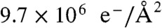 . The spatial power spectrum of the image (Fig. 4C) shows that there is sufficient information in the image to resolve the {110} hexagonal lattice plane spacing of 2.1 Å. There are 32 pores visible in the 6.27 × 10⁵ Å2 region, as indicated by the arrowheads in Fig. 4A. The locations of some of the smaller and larger pores in the image were determined by looking at preceding and subsequent images in the series where they were more easily visible. Because 1 × 10¹³ Ar+/cm2 yielded 5.1 × 10¹¹ pores/cm2, we conclude that each 3 keV Ar+ has an approximately 5% probability of nucleating a pore under these irradiation and sample conditions.
Fig. 4.

Pore nucleation and growth statistics. Electron micrograph of single-layer graphene after 1 × 10¹³ Ar+/cm2 and then 9.7 × 10⁶ e-/Å2 (A). Red arrowheads indicate locations of the 32 nanopores in the image, whose radii were measured using azimuthal integration about their center points, as quantified in the histogram (B). C shows the power spectrum of the micrograph in A, showing the hexagonal lattice of the single graphene layer.
To confirm that the argon ions created the nucleation sites leading to the pores in the images, we performed a control experiment on an identically prepared sample but without any ion bombardment (Fig. S4). For the same dose of electrons as Fig. 4, no pores were formed in a control region of the same size. The same exposure on other similar regions yielded, on average, less than one pore formed in the same area as that of Fig. 4. We attribute these occasional nucleation sites to the intrinsic defects in the graphene lattice or other beam-induced surface chemistry from a contaminant molecule.
Discussion
Our observations of nanopore formation can be understood if only atoms at the edge of the graphene are susceptible to removal by the beam. The circumference of a pore should then increase linearly with dose as edge atoms are removed. For a circular hole, one expects r = Md, where r is the radius of the pore, d is the dose in electrons/unit area, and M is the measured constant of proportionality. The linearity of radius vs. dose in our measurements supports our edge removal model of pore formation. Furthermore, we can derive the average total cross-section σe for removing the edge atoms from the slope M and the density of carbon atoms at the edge. The result is 8.9 ± 0.4 × 10⁻²⁴ cm2, where the error is the standard deviation from five measurements. Using conservative estimates of the systematic error in the measurement technique, the upper and lower bounds on this value are 9.4 and 7.5 × 10⁻²⁴ cm2, respectively (Fig. S5).
We determine the edge atom displacement energy,  , using the total cross-section formula for relativistic electron recoil off nuclei first calculated by Seitz and Koheler (25) and discussed in SI Text. We obtain an average displacement energy for edge atoms of 14.1±0.1 eV, with systematic bias bounds of 14.3 and 14.0 eV. Because an edge atom can have one of several bonding structures, this total cross-section is likely the average of several individual cross-sections times the relative probability of their occurrence on a curved graphene edge. The displacement energy for singly bonded edge atoms should be significantly lower than for double-bonded atoms. However, we expect that reconstruction and diffusion of edge atoms and vacancies likely create a largely uniform, double-bonded graphene edge (16). The measured cross-section should therefore primarily represent double-bonded edge atoms. Interior atoms are all triply bonded, hence we expect
 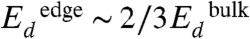 . Experimental values of
  for graphite are 20–24 eV (9), and a recent predicted value for graphene is 20 eV (10). The
  observed here is indeed approximately
  . Future experiments at lower beam energies that confirm this result would be of great interest.
Our measurements show that each 3 keV Ar+ has approximately 5% probability of nucleating a nanopore. If one assumes that a two atom defect is required for nucleation, then this measurement is consistent with atomistic simulations that predict that each ion has a 5% probability of nucleating a defect containing two missing atoms (21). The probability of a single atom defect is ten times higher. Another possible explanation for the observed pore nucleation probability is that many of the defects created by the ion beam are filled in by mobile ad-atoms created on the surface during the ion sputtering process. This ad-atom repair of defects could also explain why cooling the graphene increased the pore nucleation probability: At the temperature used (148 K), previous radiation experiments in bulk graphite indicate that ad-atom diffusion is significantly reduced (9). This reduced mobility likely prevented the induced defects from being immediately repaired by nearby mobile surface atoms created during bombardment.
The sharply peaked pore-size distribution at a particular dose shown in Fig. 4B indicates our approach would be excellent for generating monodisperse nanopores for semipermeable graphene membranes tuned to select molecules of a specific size and structure. The location and distribution of pores can be controlled by using irradiation masks or specific raster patterns (like those routinely available in a focused ion beam instrument) to limit the location of the nucleation sites. Whereas the experiments presented here used electron beams to grow and image the nanopores from nucleation sites, appropriately chosen unfocused low-energy ion beams can be used instead once the pore size vs. dose relation is known. This method makes the large-scale production of graphene nanopores much simpler and more practical because the entire process can take place in a single inexpensive apparatus where large areas or many devices can be processed in parallel.
Materials and Methods
Suspended Graphene Preparation.
Graphene was grown in our own low-pressure chemical vapor deposition system, built according to the description in ref. 19, on annealed, polycrystalline copper substrates (25 um thick, Aesar) using the procedure described in detail in Supporting Information in ref. 19. To summarize, copper foils were annealed at low pressure under continuous H2 flow at 1,000 °C for approximately 10 min, exposed to an additional flow of CH4 for approximately 10 min at 1,000 °C to grow the graphene, and then allowed to cool back to room temperature under continuous gas flow, a process which takes approximately 2 h. After growth, the graphene was transferred to gold TEM grids covered in a thin amorphous carbon film with regular arrays of micron scale holes (Quantifoil Au 1.2/2.0), using a method similar to the direct transfer method described in ref. 16. In brief, the TEM grid is placed on the graphene grown on copper foil and the carbon film is pulled into contact with the graphene by the receding interface from a deionized water droplet placed directly on the grid, which is on the substrate with the carbon film in contact with the graphene. The copper substrate is then etched away from below by floating the sample on top of FeCl3 copper etchant (Transene). Once etched, the sample is then floated in 1N HCl to remove residual iron from the FeCl3 and then floated in multiple rinses of deionized water to remove any residual salt, and dried in dry nitrogen.
At this point, we found that the samples often still contained variable amounts of surface contamination that likely formed during the growth procedure, so we developed a bake-out method to improve the sample cleanliness. TEM grids were transferred to a stainless steel UHV chamber that was just baked to 400 °C, evacuated to < 10-8 torr, and then baked overnight at 300 °C. The final pressure in the chamber after bake-out was approximately 5 × 10⁻⁹ torr. The samples were then stored in this chamber under UHV at room temperature until use. We found this procedure resulted in suspended graphene with clean regions comprising 40–80% of the graphene surface as observed in the TEM, with a typical contaminant distribution as displayed in Fig. S4.
Ion Irradiation.
To nucleate isolated atomic-scale defects in the graphene lattice, the samples were transferred to an ion sputtering system described previously (20), which is capable of irradiating samples at various temperatures with a known dose of ions under UHV conditions. The beam fluence was calibrated by measuring the count rate of the beam limited by an aperture of known size. The sample was inserted through a load-lock mechanism and then cooled to the base temperature of 148 K. The residual pressure in the chamber was < 10-9 torr, and the residual partial pressures of species up to 100 amu were monitored with an in situ residual gas analyzer (Ametek) to ensure that there were no detectable hydrocarbons, water, or other reactive species in the chamber during irradiation. To create the nucleation defect sites, the positive argon ion beam was pulsed with a duty cycle of 500 ms on 500 ms off until the sample reached the desired dose. The sample was then warmed back to 300 K and transferred to a small UHV chamber for storage until it was imaged in the electron microscope.
Electron Irradiation and Microscopy.
Before and after irradiating the sample region of interest with electrons, the electron beam current was measured with a Faraday cup integral to the sample holder (Gatan single-tilt holder), attached to a pico-ammeter (Keithley 2400), and the beam area was measured directly from an image of the sample irradiation area, which was limited by the condenser aperture. The largest contribution to systemic error is likely the beam current measurement, due to backscattering and secondary electron loss out of the 0.49 sr of exit angle subtended by the entrance to the Faraday cup. All other systematic biases are estimated to contribute < 1% error to the cross-section measurement. Residual pressure measured by the closest ion pump in the column was less than 1.3 ± 10-7 torr, and a liquid nitrogen anticontamination device in close proximity to the sample further protected it from contamination and residual water vapor in the column during electron irradiation. Objective lens aberrations were corrected to third order using a postobjective hexapole corrector, aligned to have C1 ≅ +300 Å, C3 ≅ -1 μm, and all other aberration coefficients minimized. Images were zero-loss filtered to approximately 1 eV about the primary energy of 80 keV using the in-column omega filter to improve high-resolution phase contrast by removing the inelastic electrons. Micrographs were collected on a Gatan Ultrascan 4 k camera (Harvard) or a TIVPS 4 k camera (Oberkochen) at a nominal instrument magnification of 400–800 kX or cameral length of 450 mm for selected area diffraction. For a particular experiment, the sample was irradiated continuously, and images were taken at fixed time intervals of 30 or 60 s using a postspecimen beam blanker. The total exposure time in a particular image was then determined by subtracting the image time stamp from the exposure start time. The exposure time multiplied by the beam fluence was then taken as the dose for a particular micrograph, as the beam current varied by < 2% during the course of an experiment. Atomistic Monte Carlo simulations of atomic removal were performed using our own code, which simulated the removal of atoms using our measured values of the knock-on cross-sections. Electron micrograph simulations were performed using the algorithms and code of E. Kirkland, as detailed in the reference with simulation parameters matching the experimentally measured values for our instrument (26, 27). Electron exit wave reconstruction was performed on 12 sequential images taken with 10 Å focus steps using the phase retrieval method of Gerchberg and Saxton, as implemented in the MacTempas computer simulation package. Micrographs were drift corrected using a cross-correlation algorithm (28) and postprocessed in ImageJ (29) (low-pass filter to a 1.0-Å cutoff, adjust to eight bits of linear contrast about the mean intensity value, and cropped to the region of interest). Molecular models were rendered using the visual molecular dynamics visualization package using the atomic coordinates generated in the atomistic simulations (30).
Supplementary Material
Acknowledgments.
The authors thank D. Branton for encouragement and advice during the various phases of this work, and A. Kuan for helpful comments during the preparation of this manuscript. C.J.R. acknowledges assistance with graphene growth from S. Garaj, technical assistance from R. Aubut at Harvard, A. Orchowski and D. Kolmykov at Zeiss, and advice from D.C. Bell. This work was funded by Grant R01HG003703 from the National Human Genome Research Institute, National Institutes of Health. Electron microscopy was conducted at the Harvard Center for Nanoscale Systems in Cambridge, MA and at Carl Zeiss Nano Technology Systems, GmbH in Oberkochen, Germany.
Footnotes
The authors declare no conflict of interest.
This article is a PNAS Direct Submission.
This article contains supporting information online at www.pnas.org/lookup/suppl/doi:10.1073/pnas.1119827109/-/DCSupplemental.
References
- 1.Feynman RP. Feynman and Computation: Exploring the Limits of Computers. Reading, MA: Perseus Books; 1999. pp. 67–68. [Google Scholar]
- 2.Novoselov K, et al. Electric field effect in atomically thin carbon films. Science. 2004;306:666–669. doi: 10.1126/science.1102896. [DOI] [PubMed] [Google Scholar]
- 3.Geim AK. Graphene: Status and prospects. Science. 2009;324:1530–1534. doi: 10.1126/science.1158877. [DOI] [PubMed] [Google Scholar]
- 4.Li J, et al. Ion-beam sculpting at nanometer length scales. Nature. 2001;412:166–169. doi: 10.1038/35084037. [DOI] [PubMed] [Google Scholar]
- 5.Branton D, et al. The potential and challenges of nanopore sequencing. Nat Biotechnol. 2008;26:1146–1153. doi: 10.1038/nbt.1495. [DOI] [PMC free article] [PubMed] [Google Scholar]
- 6.Garaj S, et al. Graphene as a subnanometer trans-electrode membrane. Nature. 2010;467:190–193. doi: 10.1038/nature09379. [DOI] [PMC free article] [PubMed] [Google Scholar]
- 7.Song B, et al. Atomic-scale electron-beam sculpting of near-defect-free graphene nanostructures. Nano Lett. 2011;11:2247–2250. doi: 10.1021/nl200369r. [DOI] [PubMed] [Google Scholar]
- 8.Venkatesan BM, Bashir RR. Nanopore sensors for nucleic acid analysis. Nat Nanotechnol. 2011;6:615–624. doi: 10.1038/nnano.2011.129. [DOI] [PubMed] [Google Scholar]
- 9.Kelly BT. Physics of Graphite. London: Applied Science Publishers; 1981. [Google Scholar]
- 10.Krasheninnikov AV, Banhart F. Engineering of nanostructured carbon materials with electron or ion beams. Nat Mater. 2007;6:723–733. doi: 10.1038/nmat1996. [DOI] [PubMed] [Google Scholar]
- 11.Egerton RF, Mcleod R, Wang F, Malac M. Basic questions related to electron-induced sputtering in the TEM. Ultramicroscopy. 2010;110:991–997. [Google Scholar]
- 12.Zobelli A, Gloter A, Ewels CP, Seifert G, Colliex C. Electron knock-on cross-section of carbon and boron nitride nanotubes. Phys Rev B. 2007;75:245402. [Google Scholar]
- 13.Smith B, Luzzi D. Electron irradiation effects in single wall carbon nanotubes. J Appl Phys. 2001;90:3509–3515. [Google Scholar]
- 14.Crespi V, Chopra N, Cohen M, Zettl A, Louie S. Anisotropic electron-beam damage and the collapse of carbon nanotubes. Phys Rev B. 1996;54:5927–5931. doi: 10.1103/physrevb.54.5927. [DOI] [PubMed] [Google Scholar]
- 15.Saito R, Dresselhaus G, Dresselhaus MS. Physical Properties of Carbon Nanotubes. London: Imperial College Press; 1998. [Google Scholar]
- 16.Girit CO, et al. Graphene at the edge: Stability and dynamics. Science. 2009;323:1705–1708. doi: 10.1126/science.1166999. [DOI] [PubMed] [Google Scholar]
- 17.Suenaga K, Koshino M. Atom-by-atom spectroscopy at graphene edge. Nature. 2010;468:1088–1090. doi: 10.1038/nature09664. [DOI] [PubMed] [Google Scholar]
- 18.Kotakoski J, et al. Stone–Wales-type transformations in carbon nanostructures driven by electron irradiation. Phys Rev B. 2011;83 [Google Scholar]
- 19.Reina A, et al. Large area, few-layer graphene films on arbitrary substrates by chemical vapor deposition. Nano Lett. 2009;9:30–35. doi: 10.1021/nl801827v. [DOI] [PubMed] [Google Scholar]
- 20.Stein DM, McMullan CJ, Li J, Golovchenko JA. Feedback-controlled ion beam sculpting apparatus. Rev Sci Instrum. 2004;75:900–905. [Google Scholar]
- 21.Lehtinen O, et al. Effects of ion bombardment on a two-dimensional target: Atomistic simulations of graphene irradiation. Phys Rev B. 2010;81:153401. [Google Scholar]
- 22.Lopez JJ, Greer F, Greer JR. Enhanced resistance of single-layer graphene to ion bombardment. J Appl Phys. 2010;107:104326. [Google Scholar]
- 23.Huang PY, et al. Grains and grain boundaries in single-layer graphene atomic patchwork quilts. Nature. 2011;469:389–393. doi: 10.1038/nature09718. [DOI] [PubMed] [Google Scholar]
- 24.Meyer JC, et al. The structure of suspended graphene sheets. Nature. 2007;446:60–63. doi: 10.1038/nature05545. [DOI] [PubMed] [Google Scholar]
- 25.Seitz F, Koehler JS. Displacement of atoms during irradiation. Solid State Phys. 1956;2:305–448. [Google Scholar]
- 26.Bell DC, Russo CJ, Benner G. Sub-angstrom low-voltage performance of a monochromated, aberration-corrected transmission electron microscope. Microsc Microanal. 2010;16:386–392. doi: 10.1017/S1431927610093670. [DOI] [PMC free article] [PubMed] [Google Scholar]
- 27.Kirkland EJ. Advanced Computing in Electron Microscopy. New York: Springer; 2010. [Google Scholar]
- 28.Thévenaz P, Ruttimann UE, Unser M. A pyramid approach to subpixel registration based on intensity. IEEE Trans Image Process. 1998;7:27–41. doi: 10.1109/83.650848. [DOI] [PubMed] [Google Scholar]
- 29.Rasband WS. ImageJ. Bethesda: National Institutes of Health; 1997. [Google Scholar]
- 30.Humphrey W, Dalke A, Schulten K. VMD—visual molecular dynamics. J Mol Graphics. 1996;14:33–38. doi: 10.1016/0263-7855(96)00018-5. [DOI] [PubMed] [Google Scholar]
Associated Data
This section collects any data citations, data availability statements, or supplementary materials included in this article.