Abstract
Carbon nanotubes (CNTs) are well-known as materials for nanoelectronics and show great potential to be used as the sensing element in chemical and biological sensors. Recently, CNTs have been shown to be effective nanofluidic channels and the transport of substances through small diameter CNTs is intrinsically fast, selective, and operates at the single molecule level. It has been shown that the transport characteristics of semiconducting single-walled CNT (SWCNT) field effect transistor (FET) are sensitive to internal water wetting. We report here that the characteristics of semiconducting SWCNT FETs are also sensitive to the concentration, pH and ion type of ionic solution when the electrolytes are inside the CNT. Such sensitivity is not observed at the outside surface of a semiconducting SWCNT. This opens a new avenue for building new types of CNT sensor devices in which the SWCNT concurrently functions as a nanochannel and an electronic detector.
Keywords: nanofluidics, nanopore, nanochannel, carbon nanotube, CNT FET, chemical and biosensor
1. Introduction
CNTs are excellent one-dimensional electronic materials with a large surface-to-volume ratio. It has been demonstrated that the electronic properties of SWCNTs and the Schottky barriers between SWCNTs and metal contacts are very sensitive to adsorbates [1, 2] and the environment [3-5], which is the basis of many CNT field effect transistor (FET) chemical and biological sensors. In recent years, carbon nanotubes (CNT) have also been employed as nanopores or nanochannels to rapidly transport a variety of ions and molecules, both in gas and liquid phases [6-10] [11]. It is appealing to integrate the nanoelectronic and nanofluidic advantages of SWCNT into one device. Such integration will enable electrical probing of the activities confined in extremely small spaces in situ and in real time. The high electronic sensitivity of CNTs to charged ions and molecules in their proximity can be readily utilized to study the dynamics of ion and molecule translocation processes in sub 2nm channels, a regime not previously studied experimentally. In addition, this investigation may lead to a new type of CNT sensor with enhanced sensitivity.
We have built a combined CNT-nanopore- FET device. The internal wetting of semiconducting SWCNTs by pure water significantly modifies the FET characteristics [7, 12]. In contrast, external wetting has little effect. Theoretical simulations revealed that internal water forms ordered structure, both generating a large dipole electric field, causing charge polarization of the tube and contacting metal electrodes, and shifting the valance band of the SWCNT. External water has little effect because external water molecules are randomly oriented and the interactions between external water molecules and the outside surface of the CNT are weaker. Recent experimental work has used such sensitivity to probe the average speed of water molecules when moving inside a semiconducting SWCNT [11]. In this report, we examined the electrical response of SWCNT when its interior was exposed to aqueous solution with various ion concentrations, pH and ion species. High sensitivity was observed for semiconducting SWCNT FET only when the internal surface of SWCNT was exposed to electrolytes. This is a continuation of previous water wetting work and one step closer to the goal of a functional nano-electrofluidic device. There is a recent trend to develop conductive synthetic nanopores, which are capable in controlling the electrostatic environment of the pore for biomolecule manipulation and enriching electrical sensing methods [13]. The conductive nanopores have been made by either metallization of insulating pore [14, 15] or directly using conductive materials, such as graphene [16-18]. The current work on conductive CNT nanopore will contribute significantly to the research in this area.
2. The experiment
The device structure and experiment setup are illustrated in Figure 1. The device fabrication has been described in details in previous report [7, 12]. Briefly, long SWCNTs with average outer diameter of 1.7nm were grown by the chemical vapor deposition method on a highly doped silicon substrate with a 1μm thick SiO2 top layer. Gold source and drain electrodes were fabricated by electron-beam lithography (EBL) to directly contact one SWCNT under the PMMA barrier (20-40μm in width). The heavily doped silicon substrate was used as a back gate. SWCNTs were characterized as semiconducting or metallic based on measurements of source-drain current (Ids) versus backgate voltage (Vg), which were measured by a Keithley 2636A (Keithley Instruments, Inc., Ohio). A clean PDMS stamp with imbedded microfluidic channels sealed the surface of the CNT chip to deliver electrolytes (Figure 1a and c) into CNT. An Axon 200B (Molecular Devices, Inc., CA) in voltage clamp mode was used to measure the ionic current between two reservoirs (as bridged by only one SWCNT) using Ag/AgCl electrodes (MF-2078, BAS, 2M KCl). All the electrical measurements were carried out on a home-built probe station inside a Faraday cage.
Figure 1.
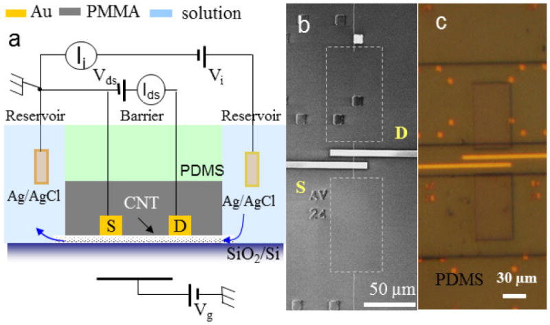
(a) Schematic of the device structure of a combined SWCNT field effect transistor and nanopore device. The electrical measurement configuration for both electronic current and ionic current measurement is also shown. The distances between source (S) and drain (D) electrodes is 15μm and the barrier width is 30μm. (b) Scanning electron microscope (SEM) image of a used device after stripping off the covering PMMA layer. The two rectangles enclosed by white dash lines indicate the location of reservoirs. In the barrier region, one SWCNT bridges two reservoirs and is also contacted by both the source and drain electrodes. (c) Optical microscope image of a working device during measurement. The device is covered by a PDMS stamp with microfluidic channels and aqueous solution fills the reservoirs.
We have fabricated 11 functional devices, of which 8 were semiconducting SWCNTs and 3 were metallic SWCNTs. All the devices made from metallic SWCNTs display negligible change in IdsVg curves compared with the devices with semiconducting SWCNT (see the supplementary information). For controls, we always examine the working devices prior to opening the CNT using an oxygen plasma. We also prepare control devices with a section of SWCNT between source and drain electrodes exposed to various electrolytes (Figure S2). None of these controls alter the transport characteristics of the SWCNT FET significantly. After removing the exposed CNT in the reservoirs (see Figure 1b) and opening the ends of CNT by oxygen plasma, 6 devices made with semiconducting SWCNTs show the same trend of variation in IdsVg curves when exposed to electrolytes with various concentration, pH and ion species. The other 2 devices don’t display systematic and repeatable responses, which may due to defects or contaminations in the devices. In the following paragraphs, we will only discuss the results from those 6 devices.
3. Results and discussion
We first measured IdsVg curves of SWCNT FET devices in KCl solution with different concentrations and the results for three devices are shown in Figure 2a-c. The curves have hysteresis and only the sweep-down curves are shown. The electronic transport measurement in air (grey curves) suggested the FET was p-type, which is “on” at negative gate voltage and “off” at positive gate voltage. After adding DI-water, the device became insensitive to the back gate voltage, keeping Ids constant for the entire range of Vg (green curves) as previously reported [12]. We then studied the response of the SWCNT FET when KCl solutions with different concentrations were injected into the reservoirs sequentially in an order from low to high. The IdsVg curves changed correspondingly with KCl concentration but the change was not monotonic. With the increase of KCl concentration from 1×10⁻⁵M to 1M, the Ids at positive gate bias (e.g., at 10V) current initially decreased, restoring the p-type behavior, and then increased again. The current at negative gate bias (saturation current) hardly changed for all the KCl solutions. To better display the results, we define gating efficiency, ΔI/I-. Here, ΔI= I- - I+, where I+ is the maximum current at positive gate voltage and I- is the maximum current at negative gate voltage. The plot of ΔI/I- vs. KCl concentration is shown in Figure 2d. To reveal the device to device variation, the results for 4 devices are shown here. It is obvious that the ratio is the biggest at around 0.1mM. When the KCl concentration is further increased, the gating efficiency decreases in general though there are device to device variations. The corresponding controls do not show this level of sensitivity to salt concentration. The ionic current through device 1 has also been measured at different KCl concentrations (gray curve in Figure 2d), showing similar behavior as previously reported [7]. These results confirm that the inner surface of semiconducting SWCNT is electrically sensitive to ions. At low salt concentration, the presence of ions likely disrupts the orderly oriented water structure inside the CNT and suppresses the interaction between water and the inner surface of SWCNT. So we observe the increase of gating efficiency until the salt concentration reaching 10-4M. At higher salt concentration, the gate voltage will be strongly screened by the ionic solution inside the CNT and thus the gating efficiency is reduced.
Figure 2.
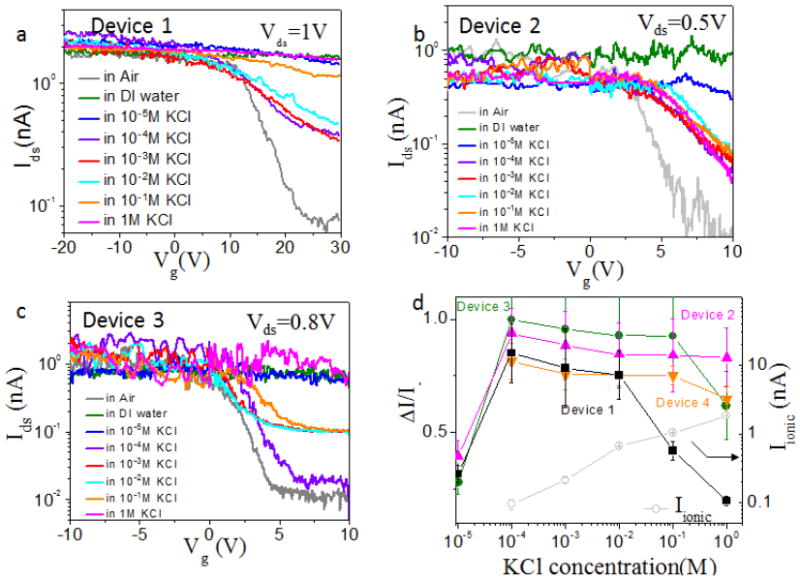
The dependence of electronic and ionic current on KCl concentration. (a)-(c) Ids-Vg semilog curves of 3 working devices with opened semiconducting SWCNTs before (gray) and after adding DI water (green) and 1×10⁻⁵ M to 1M KCl (pH=7) solutions sequentially from low to high. (d) Gating efficiency ΔI/I- vs. KCl concentration for 4 different devices. The ionic current (gray) at Vionic=0.5V and at different KCl concentration is also shown here for comparison.
We further studied the response of the electrical transport characteristics of the SWCNT FET when exposed to ionic solution with different pH values. Figure 3a-c showed IdsVg curves for three opened semiconducting SWCNT FET devices when the reservoirs were filled with 1mM KCl solutions at various pH values from 3 to 9. The Ids at positive gate voltage (i.e., 10V) increased significantly at low pH while the Ids at negative gate voltage were relatively constant. KCl solution at higher concentration such as 1M was also tested and the pH sensitivity was much lower (e.g., 1M, see supporting information). The pH dependence of the electrical transport characteristics was also reflected in the gating efficiency ΔI/I- vs. pH plots (Figure 3d). The biggest gating efficiency appeared at pH 9, where Ids+ was the lowest. Using a liquid-gated FET configuration, recent studies often reported the SWCNT conductance (at a fixed gate voltage) increased with the increase of solution pH [19-22]. This response was opposite to that of the opened SWCNT FET, suggesting different mechanisms for pH sensitivity between opened and unopened SWCNT FETs. The pH sensitivity for the unopened SWCNT was attributed to the adsorption of hydroxyl groups to the external surface of SWCNT or the ionization of silanol groups on SiO2 surface near the SWCNT. In our control experiments (supporting information), the exterior surface of CNT didn’t show any sensitivity, differing significantly from the opened CNT. In order to better understand the pH sensitivity of opened SWCNT, we also measured the ionic current through CNT in 1mM KCl solution at different pH (gray curve in Figure 3d). The ionic current increased with the increase of pH, which was consistent with previous results and was attributed to protonation of carboxyl groups at CNT ends [7]. At pH 9, positive potassium ions are in excess within the CNT. Considering both the Ids and ionic conductance data, we propose one explanation for the experimental data. When the KCl concentration is low, proton and potassium ions are the major carriers inside the CNT at pH 3 and 9 respectively. At pH 3, the FET gating efficiency is suppressed by effective water-CNT interior interaction due to the reduced number of potassium ions [12]. At pH 9, positive potassium ions are excess inside the CNT and disrupt the water-CNT interaction more frequently and therefore restore the gating efficiency. This hypothesis is supported by the fact that the pH sensitivity almost disappears at 1M KCl concentration because the number of potassium ions are large even at pH 3 solution. It is also worth to note that the opposite trend between Ids+ and ionic current as a function of pH excludes the possibilities of a short circuit between drain and source electrodes caused by interior conductive ionic solution.
Figure 3.
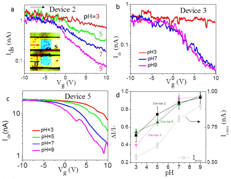
pH dependence of 3 working device containing open ends (semiconducting SWCNTs). (a)-(c) Ids-Vg semilog curves for three devices filled sequentially with pH=3 (red), pH=5 (green), pH=7 (blue) and pH=9 (magenta) 1mM KCl solutions at Vds=0.5V. The inset in (a) shows an optical image of a device sealed with a PDMS cover with microfluidc channels (green). The two blue squares (i.e., 60 μm × 60 μm) are the fluid reservoirs cut into the PMMA (yellow). (d) Gating efficiency ΔI/I- for different pH (black solid squares) for 3 devices. The measured ionic current at different pH was shown (gray open circles). The concentration of the KCl solution is 1mM and Vionic= 0.5V.
We also studied the electrical sensitivity of the opened semiconducting SWCNT to chloride electrolytes with three different cations, K+, Na+ and Li+. We used 1mM for concentration to optimize sensitivity. The electrolytes are freshly prepared and no buffer is added to make the electrolytes as simple as possible. As shown in Figure 4a, the biggest change in Ids as a function of Vg is observed for the electrolyte containing K+, which has the largest atomic size but the smallest hydration shell out of the three tested cations. The gating efficiencies ΔI/I- in various 1mM chloride electrolytes are also illustrated in Figure 4b. Same to Figure 4a, the biggest gating efficiency is obtained in KCl solution. These results confirm that the interaction between water molecules and CNT inner surface is more critical in determining Ids+. Stronger interaction will more effectively diminish the device gating efficiency. Potassium ion is likely more effective in preventing the effective interaction between water molecules and CNT inner surface due to its bigger atomic size. We also measured the ionic current through the opened SWCNT. For comparison, the ionic current only through the PDMS microfluidic channels (minimum width >10μm) was measured and the conductance values were close to the bulk solution data. As shown in Figure 4b, the ionic conductance in both SWCNT nano channel and PDMS micron channel varied in the sequence GKCl>GNaCl>GLiCl. However, the ionic conductance of LiCl solution is about 0.8 of KCl solution in micro channels and drops to about 0.3 in SWCNT nano channels. The difference suggests the potassium ion is easier to be translocated through the SWCNT, attributing to its smaller hydration size. The ratio of GLiCl/GKCl varied from 0.3 to 0.6 for different SWCNT devices. The variation presumably arises from the fluctuation of SWCNT diameters. Our results are also consistent with the observation of substantial ion selection in sub 2nm CNTs[23]. The origin of ion selection has been confirmed as the steric exclusion by the small CNT diameter and the electrostatic rejection by the carboxyl groups at CNT ends [23].
Figure 4.
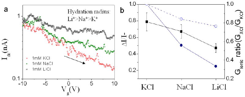
The electrical response of opened semiconducting SWCNTs to different cations. (a) Typical Ids vs. Vgs curves when the opened SWCNT (device 2) was exposed to 1mM KCl (red), NaCl (green) and LiCl (black) solutions respectively at Vds=0.5V. (b) Gating efficiency ΔI/I-(black squares) and ionic conductance ratio (normalized with GKCl) (blue solid circles) in three different 1mM ionic solutions for the same SWCNT device are shown. The ionic conductance ratios in PDMS micron size channels are also displayed for comparison (blue open circles).
Finally, we studied the electrical response with time. As shown in Figure 5, the device can response to the in situ exchange of concentration (Fig. 5 a and b) and pH (Fig.5 c and d) of the KCl solutions in the reservoirs. The response is reversible. Due to the microfluidic channel design, it normally takes several seconds to exchange the solution in the reservoirs. During the solution exchange, the electrical current Ids is often affected by mechanical vibrations. Therefore, we cannot acquire the response time of the device accurately. However, we consistently observe that the device responds more quickly when the conductivity of SWCNT is changed from high to low than from low to high, for both concentration and pH.
Figure 5.
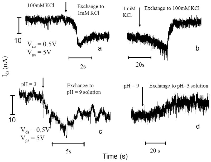
The electrical response of an open ends semiconducting SWCNT to different concentration and pH KCl solutions as a function of time. (a) and (b) Ids vs. t traces when the opened SWCNT was exposed to 100 mM and 1mM KCl solutions sequentially at Vds=0.5V and Vgs=5V. The pH was7 in this case. (c) and (d), Ids vs. t traces when the opened SWCNT was exposed to pH=3 and pH=9 solutions sequentially at Vds=0.5V and Vgs=5V. The KCl concentration is fixed at 1mM. The arrows indicate the starting points of solution exchange by syringe.
4. Conclusion
Our experiments demonstrated that the electronic properties of semiconducting SWCNTs are highly sensitive to the variations of ionic flow inside the SWCNT. This will be important for developing a fundamental understand of the dynamics of ion and molecule transport through sub-2nm conductive nanopores and nanochannels and the induced polarization effect inside conductive nanopores. In addition, the results reported here are one step further towards building new type of nano-electrofluidic devices and platforms for biomolecule manipulation and detection. Using the same device structure, the electronic sensitivity to small charged (bio) molecules will be studied in the next step. Single molecule sensitivity is expected.
Supplementary Material
Acknowledgments
We thank Tao Luo and Weishi Song for assistance in the lab. We acknowledge valuable discussions with Dr. Kristic Predrag. We also acknowledge the use of nanofab within Center for Solid State electronic research (CSSER) and SEM and TEM within the Center for Solid State Science (CSSS) at Arizona State University. This work was supported by the DNA Sequencing Technology Program of the National Human Genome Research Institute (1RC2HG005625-01, 1R21HG004770-01) and the Biodesign Institute.
References
- 1.Staii C, Johnson AT, Chen M, Gelperin A. DNA-Decorated Carbon Nanotubes for Chemical Sensing. Nano Letters. 2005;5:1774–8. doi: 10.1021/nl051261f. [DOI] [PubMed] [Google Scholar]
- 2.Star A, Gabriel J-CP, Bradley K, Gruner G. Electronic Detection of Specific Protein Binding Using Nanotube FET Devices. Nano Letters. 2003;3:459–63. [Google Scholar]
- 3.Douglas RK, Alexander S. Carbon Nanotube Gas and Vapor Sensors. Angewandte Chemie International Edition. 2008;47:6550–70. doi: 10.1002/anie.200704488. [DOI] [PubMed] [Google Scholar]
- 4.Heller I, Mannik J, Lemay SG, Dekker C. Optimizing the Signal-to-Noise Ratio for Biosensing with Carbon Nanotube Transistors. Nano Letters. 2009;9:377–82. doi: 10.1021/nl8031636. [DOI] [PubMed] [Google Scholar]
- 5.Cui X, Freitag M, Martel R, Brus L, Avouris P. Controlling Energy-Level Alignments at Carbon Nanotube/Au Contacts. Nano Letters. 2003;3:783–7. [Google Scholar]
- 6.Hinds BJ, Chopra N, Rantell T, Andrews R, Gavalas V, Bachas LG. Aligned Multiwalled Carbon Nanotube Membranes. Science. 2004;303:62–5. doi: 10.1126/science.1092048. [DOI] [PubMed] [Google Scholar]
- 7.Liu H, He J, Tang J, Liu H, Pang P, Cao D, Krstic P, Joseph S, Lindsay S, Nuckolls C. Translocation of Single-Stranded DNA Through Single-Walled Carbon Nanotubes. Science. 2010;327:64–7. doi: 10.1126/science.1181799. [DOI] [PMC free article] [PubMed] [Google Scholar]
- 8.Holt JK, Park HG, Wang YM, Stadermann M, Artyukhin AB, Grigoropoulos CP, Noy A, Bakajin O. Fast mass transport through sub-2-nanometer carbon nanotubes. Science. 2006;312:1034–7. doi: 10.1126/science.1126298. [DOI] [PubMed] [Google Scholar]
- 9.Lee CY, Choi W, Han J-H, Strano MS. Coherence Resonance in a Single-Walled Carbon Nanotube Ion Channel. Science. 2010;329:1320–4. doi: 10.1126/science.1193383. [DOI] [PubMed] [Google Scholar]
- 10.He J, Liu H, Pang P, Cao D, Lindsay S. Translocation events in a single-walled carbon nanotube. Journal of Physics-Condensed Matter. 2010;22 doi: 10.1088/0953-8984/22/45/454112. [DOI] [PMC free article] [PubMed] [Google Scholar]
- 11.Qin X, Yuan Q, Zhao Y, Xie S, Liu Z. Measurement of the Rate of Water Translocation through Carbon Nanotubes. Nano Lett. 2011;11:2173–7. doi: 10.1021/nl200843g. [DOI] [PubMed] [Google Scholar]
- 12.Cao D, Pang P, He J, Luo T, Park JHP, Krstic P, Nuckolls C, Tang JT, Lindsay S. Electronic sensitivity of carbon nanotubes to internal water wetting. ACS Nano. 2011;5:3113–9. doi: 10.1021/nn200251z. [DOI] [PMC free article] [PubMed] [Google Scholar]
- 13.Jiang Z, Stein D. Electrofluidic Gating of a Chemically Reactive Surface. Langmuir. 2010;26:8161–73. doi: 10.1021/la9044682. [DOI] [PubMed] [Google Scholar]
- 14.Nishizawa M, Menon VP, Martin CR. Metal Nanotubule Membranes with Electrochemically Switchable Ion-Transport Selectivity. Science. 1995;268:700–2. doi: 10.1126/science.268.5211.700. [DOI] [PubMed] [Google Scholar]
- 15.Wei R, Pedone D, Zürner A, Döblinger M, Rant U. Fabrication of Metallized Nanopores in Silicon Nitride Membranes for Single-Molecule Sensing. Small. 2010;6:1406–14. doi: 10.1002/smll.201000253. [DOI] [PubMed] [Google Scholar]
- 16.Schneider GF, Kowalczyk SW, Calado VE, Pandraud G, Zandbergen HW, Vandersypen LMK, Dekker C. DNA Translocation through Graphene Nanopores. Nano Letters. 2010;10:3163–7. doi: 10.1021/nl102069z. [DOI] [PubMed] [Google Scholar]
- 17.Napoli M, Eijkel JCT, Pennathur S. Nanofluidic technology for biomolecule applications: a critical review. Lab on a Chip. 2010;10:957–85. doi: 10.1039/b917759k. [DOI] [PubMed] [Google Scholar]
- 18.Merchant CA, Healy K, Wanunu M, Ray V, Peterman N, Bartel J, Fischbein MD, Venta K, Luo Z, Johnson ATC, Drndic M. DNA Translocation through Graphene Nanopores. Nano Letters. 2010;10:2915–21. doi: 10.1021/nl101046t. [DOI] [PubMed] [Google Scholar]
- 19.Back JH, Shim M. pH-Dependent Electron-Transport Properties of Carbon Nanotubes. The Journal of Physical Chemistry B. 2006;110:23736–41. doi: 10.1021/jp063260x. [DOI] [PubMed] [Google Scholar]
- 20.Matthew RL, Canan S, Tal S, Josh K, Vincent TR, Ethan DM. Fabrication and characterization of carbon nanotube field-effect transistor biosensors. In: Ruth S, Ioannis K, editors. SPIE. 2010. p. 77790H. [Google Scholar]
- 21.Huang S-CJ, Artyukhin AB, Misra N, Martinez JA, Stroeve PA, Grigoropoulos CP, Ju J-WW, Noy A. Carbon Nanotube Transistor Controlled by a Biological Ion Pump Gate. Nano Letters. 2010;10:1812–6. doi: 10.1021/nl100499x. [DOI] [PubMed] [Google Scholar]
- 22.Heller I, Chatoor S, Männik J, Zevenbergen MAG, Dekker C, Lemay SG. Influence of Electrolyte Composition on Liquid-Gated Carbon Nanotube and Graphene Transistors. Journal of the American Chemical Society. 2010;132:17149–56. doi: 10.1021/ja104850n. [DOI] [PubMed] [Google Scholar]
- 23.Fornasiero F, Park HG, Holt JK, Stadermann M, Grigoropoulos CP, Noy A, Bakajin O. Ion exclusion by sub-2-nm carbon nanotube pores. Proceedings of the National Academy of Sciences. 2008;105:17250–5. doi: 10.1073/pnas.0710437105. [DOI] [PMC free article] [PubMed] [Google Scholar]
Associated Data
This section collects any data citations, data availability statements, or supplementary materials included in this article.


