Abstract
Printed electronics rely on low-cost, large-area fabrication routes to create flexible or multidimensional electronic, optoelectronic, and biomedical devices1-3. In this paper, we focus on one- (1D), two- (2D), and three-dimensional (3D) printing of conductive metallic inks in the form of flexible, stretchable, and spanning microelectrodes.
Direct-write assembly4,5 is a 1-to-3D printing technique that enables the fabrication of features ranging from simple lines to complex structures by the deposition of concentrated inks through fine nozzles (~0.1 - 250 μm). This printing method consists of a computer-controlled 3-axis translation stage, an ink reservoir and nozzle, and 10x telescopic lens for visualization. Unlike inkjet printing, a droplet-based process, direct-write assembly involves the extrusion of ink filaments either in- or out-of-plane. The printed filaments typically conform to the nozzle size. Hence, microscale features (< 1 μm) can be patterned and assembled into larger arrays and multidimensional architectures.
In this paper, we first synthesize a highly concentrated silver nanoparticle ink for planar and 3D printing via direct-write assembly. Next, a standard protocol for printing microelectrodes in multidimensional motifs is demonstrated. Finally, applications of printed microelectrodes for electrically small antennas, solar cells, and light-emitting diodes are highlighted.
Keywords: Bioengineering, Issue 58, Direct-write assembly, silver ink, 3D printing, planar, three-dimensional, microelectrodes, flexible electronics, printed electronics
Protocol
1. Introduction
This paper demonstrates the 1D, 2D, and 3D printing of conductive microelectrodes via direct-write assembly.
Direct-write assembly is a method of building up 1D-to-3D printed structures by the deposition of concentrated inks through fine nozzles.
Our system consists of a computer-controlled 3-axis translation stage, an ink reservoir and nozzle, and 10x telescopic lens for imaging (Figure 1).
Direct-write assembly is a filamentary printing approach in which concentrated inks are extruded through cylindrical nozzles, whose diameters range from 0.1 to 250 μm (Figure 2). Notably, due to the viscoelastic ink characteristics, direct-write assembly enables self-supporting spanning features (Figure 3). To date, a wide range of inks, including those composed of ceramic6,7, organic8-10, metallic11-15, polymeric16,17, and sol-gel18,19 materials have been developed for this printing approach (Figure 4).
2. Preparation of highly concentrated silver nanoparticle inks
Silver nanoparticle inks are prepared by first dissolving a blend of 5,000 and 50,000 molecular weight of poly(acrylic acid) in a mixture of 50 g water and 40 g diethanolamine (Video 2.1).
The polymer acts as a capping agent to control the size of the silver nanoparticles.
Next, an aqueous solution of silver nitrate is injected into the polymer solution. After addition, a light yellow transparent solution is obtained (Video 2.2).
After stirring for 24 hrs at room temperature, the solution develops a reddish-brown color (Video 2.3), that coincides with the formation of silver nanoparticles of 5 nm diameter, as determined by transmission electron microscopy.
Next, the solution is sonicated at 65 °C in a water bath for 2 hrs for further particle growth (Video 2.4).
After sonication, the solution is transferred to a 500 ml beaker and cooled to room temperature. Then, 300 ml of ethanol is titrated at a rate of 30 ml / min. Since ethanol is a poor solvent for the poly(acrylic acid) capping agent, the particles rapidly coagulate and precipitate from solution (Video 2.5).
After decanting the supernatant, the precipitate is collected into a centrifuge tube and centrifuged at 9000 rpm for 20 minutes (Video 2.6).
After this step, a highly concentrated silver nanoparticle ink with a solids loading of ~85 wt% is obtained (Video 2.7).
Further control over ink viscosity and elastic modulus can be achieved by dilution, followed by homogenization. For an example, a humectant solution, such as ethylene glycol, can be added to the ink and then homogenized at 2000 rpm for 3 minutes using a Thinky homogenization mixer. After this process, a uniform ink of a bluish to magenta color is obtained (Video 2.8).
The TEM image shows silver nanoparticles obtained by this synthesis procedure (Figure 5_left). The particles have a mean diameter of 20 nm with a size distribution of 5-50 nm. Printed structures require post-annealing to enhance their conductivity. After annealing at 250°C for less than 30 min, the silver nanoparticles form conductive microelectrodes with an electrical resistivity approaching to 10-5 Ω•cm (Figure 5_bottom right). The microstructural evolution of the printed silver microelectrodes as a function of annealing temperature is shown in Figure 5_top right. As the temperature increases from 150° to 550°C, the microelectrodes undergo densification with a total volumetric shrinkage of ~30%.11
The ink rheology, which strongly depends on its solids loading, determines its printability. The ink viscosity increases with increasing solids loading (Figure 6). Because dilute inks with low viscosity result in a significant lateral spreading, concentrated inks with a solids loading ranging from 70 to 85 wt% are required for printing of planar and spanning ink filaments.
The ink elastic modulus increases with increasing solids loading (Figure 7). In the linear viscoelastic region, the elastic modulus rises nearly three orders of magnitude as the solids loading increases 60 to 75 wt%. A minimum elastic modulus of 2000 Pa is required to produce self-supporting or spanning features.
3. Direct-write assembly
Direct-write assembly is carried out by first loading the ink into a syringe barrel. After attaching a deposition nozzle, the ink-loaded syringe barrel is mounted onto the 3-axis printing stage (Video 3.1).
Using a computer program, arbitrary designs, including linear, planar, and complex three-dimensional structures can be easily generated (Video 3.2).
Next, the nozzle height is adjusted with the aid of telescope lens with a 10x zoom (Video 3.3).
After applying pressure using an air-powered fluid dispensing system, the ink is deposited onto the substrate with a controlled printing speed (Video 3.4). The required pressure depends upon ink rheology, nozzle diameter, and printing speed, but typical values range from 10-100 psi at 20-500 μm/s. This printing is performed in air at room temperature. Using this printing procedure, the printing of silver microelectrodes in different layouts and size scales is demonstrated.
For an example, the printing of conductive silver grids with a center-to-center line spacing of 100 μm, patterned by a 5-μm nozzle on a silicon wafer substrate is demonstrated (Video 3.5).
In addition, this video shows how to create a high aspect ratio cylindrical structure by a 30-μm nozzle using a layer-by-layer printing method (Video 3.6).
Furthermore, the omnidirectional printing of silver microelectrodes between two glass substrates offset by a 1-mm height difference is demonstrated using a 30-μm nozzle (Video 3.7).
Completely free-standing, vertically printed silver microspikes can be created by a 30-μm nozzle on a Si wafer substrate (Video 3.8).
Finally, this video shows direct writing of a spanning silver microelectrode using a 10-μm nozzle (Video 3.9). The printed feature can span distances up to one centimeter with minimal drooping or buckling.
4. Representative results:
We prepared a highly concentrated silver nanoparticle inks and demonstrated printed conductive features in planar and 3D motifs for electronic and optoelectronic applications with printing resolution ~ 2 - 30 μm. For an example, Figure 8 exhibits the printing resolution of this technique. Printed features with minimum electrode width of ~ 2 μm (1.4 μm thick) are obtained in a single pass using a 1-μm nozzle11.
Figure 9 shows transparent conductive silver grids, patterned by a 5 μm nozzle on a flexible polyimide film12. The texts underneath the printed grids are clearly visible. These transparent silver grids could be attractive alternatives for transparent conducting oxide (TCO) materials.
Conformal printing onto a non-planar substrates is also enabled by this method. Figure 10 demonstrates the conformal printing of a 3D electrically small antenna. A 100 μm metal nozzle is used to print meander-line patterns on the surface of a glass hemisphere13. This approach may find several applications including implantable and wearable antennas, electronics, and sensors.
Applications of spanning silver microelectrodes in three-dimensional photovoltaics and light-emitting diodes are demonstrated (Figure 11-14).
First, Figure 11 is an example of silicon spherical shell. This tenuous film with a 2-μm thickness can be wire-bonded to an external circuit by omnidirectional printing14. This method uses minimal contact pressure, which is highly advantageous for delicate devices.
Next, Figure 12 demonstrates an example of printing a spanning interconnect for a silicon solar microcell array in which silicon microribbon elements are separated by 33-μm gap15.
Next, Figure 13 shows silver interconnects for the gallium arsenide-based LED array with 4-by-4 pixels, where each pixel (500 x 500 x 2.5 μm3) is spaced 200 μm apart11. The bottom image displays the LED array, emitting uniform red light under an applied bias of 6 V from a single pixel. The ability to print spanning electrodes enables multilayer interconnection without the use of supporting or sacrificial layers (top images).
As a final demonstration, Figure 14 shows SEM images for the complex 3D microperiodic silver lattice printed by a 5μm nozzle.
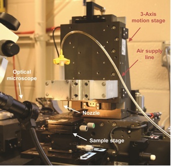 Figure 1. Optical image of direct ink writing apparatus.
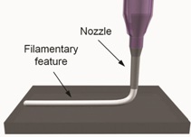 Figure 2. Direct ink writing of a filamentary feature.
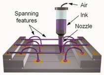 Figure 3. Direct ink writing of self-supporting spanning features.
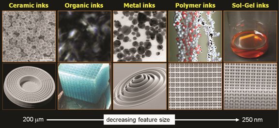 Figure 4. Ink designs for direct ink writing. A wide range of concentrated viscoelastic inks have been developed for direct writing of planar and complex 3D structures with microscale features.
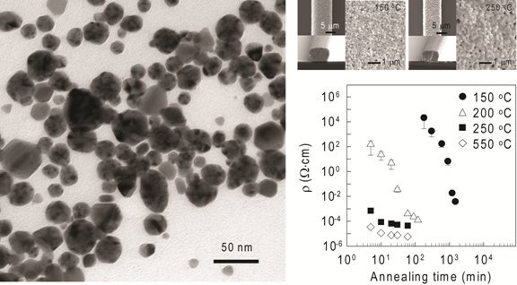 Figure 5. (Left) Transmission electron microscopy (TEM) image of silver nanoparticles. (Top right) SEM images of silver microelectrodes patterned with a 15-μm nozzle as a function of annealing temperature. (Bottom right) Electrical resistivity of silver microelectrodes as a function of annealing temperature and time.
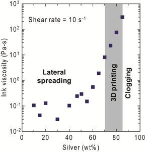 Figure 6. Apparent viscosity (η) of the silver nanoparticle inks as a function of solids loading.
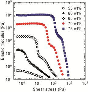 Figure 7. Shear elastic modulus (G') as a function of shear stress for silver nanoparticle inks of varying solids loading.
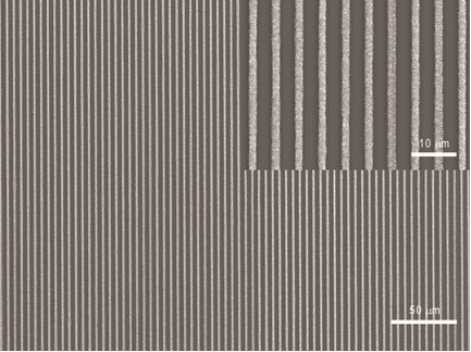 Figure 8. SEM images of planar arrays of silver microelectrodes patterned on a Si wafer with a 1-μm nozzle.
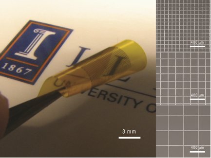 Figure 9. Optical image of transparent conductive silver grids (left) and SEM images of the grids printed as a function of line pitch (right).
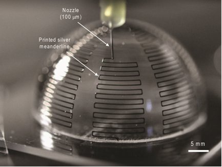 Figure 10. Optical image captured during conformal printing of electrically small antennas on a hemispherical glass substrate.
 Figure 11. Optical image obtained during printing of spanning silver microelectrodes onto a thin (2-μm) silicon spherical shell.
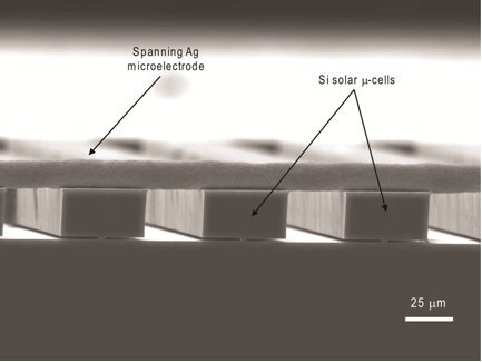 Figure 12. SEM image of a spanning silver microelectrode printed onto a silicon solar microcell array.
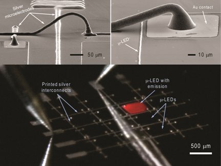 Figure 13. SEM images (top) and optical image (bottom) of a 4-by-4 LED chip array interconnected by silver microelectrodes.
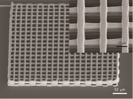 Figure 14. SEM image of 3D microperiodic silver lattice.
Discussion
Conventional droplet-based printing approaches, such as inkjet printing, are limited to the fabrication of planar electrodes with low aspect ratio due to the dilute nature and low viscosity of the inks used. Recently, dip-pen nanolithography (DPN)20-22 and e-jet printing23-25 have been used to pattern conductive features. These routes also employ dilute, low viscosity inks. Pearton and co-workers used DPN to deposit a commercially available silver nanoparticle ink at write speeds of up to 1600 μm s-1 and line widths of approximately 0.5 μm22. However, fabrication of reproducible patterns over large areas has yet to be demonstrated by this approach. Silver nanoparticle inks have also been deposited by e-jet printing to form conductive traces with line widths of ~ 1.5 μm25. However, as with inkjet printing, inhomogeneous printed features may arise due to satellite drop formation and non-uniform drop drying24,25.
As demonstrated above, direct-write assembly of concentrated silver nanoparticle inks overcomes these limitations through a filamentary-based printing approach. This technique enables the fabrication of conductive microelectrodes with a high aspect ratios (h/w ≈ 1.0) in a single passes allowing the creation of 1D, 2D, and 3D architectures. The size of the printed features depends upon nozzle diameter, ink solids loading, applied pressure, and printing speed. To date, conductive traces as small as ~ 2 μm have been patterned using a 1 μm nozzle at modest speeds (< 2 mm s-1). By tailoring the ink composition and nozzle geometry, maximum printing speeds in excess of 10 cm s-1 are possible. However, high speed printing of using fine nozzles (< 5 μm) remains a significant challenge.
To demonstrate applications of direct-write assembly, we fabricated conductive grids, electrically small antennas, solar cells, and light-emitting diodes with planar and spanning printed electrodes (Figure 8-14). Notably, our approach is not restricted to the creation of metallic structures. Using other ink designs, such as those based on silk fibroin, hydrogel and fugitive organic inks, we have constructed 3D scaffolds and microvascular networks for tissue engineering and cell culture via direct-write assembly26-30.
Looking towards the future, there are many opportunities and challenges. Further advances require new ink designs, better modeling of ink flow dynamics, and enhanced robotic and control systems. Large-area fabrication of 1D to 3D structures with high throughput and nanoscale resolution (< 100 nm) remains a significant challenge.
Disclosures
No conflicts of interest declared.
Acknowledgments
This material is based on work supported by the U.S. Department of Energy, Materials Sciences and Engineering Division (Award No. DEFG-02-07ER46471) and the DOE Energy Research Center on Light-Materials Interactions in Energy Conversion (Award No. DE-SC0001293), and benefitted from access to the Center for Microanalysis of Materials within the Frederick Seitz Materials Research Laboratory (FSMRL).
References
- Chrisey DB. The power of direct writing. Science. 2000;289:879–881. doi: 10.1126/science.289.5481.879. [DOI] [PubMed] [Google Scholar]
- Sirringhaus H. High-resolution inkjet printing of all-polymer transistor circuits. Science. 2000;290:2123–2126. doi: 10.1126/science.290.5499.2123. [DOI] [PubMed] [Google Scholar]
- Kim R-W. Waterproof AllnGaP optoelectronics on stretchable substrates with applications in biomedicine and robotics. Nat. Mater. 2010;9:929–937. doi: 10.1038/nmat2879. [DOI] [PubMed] [Google Scholar]
- Lewis JA, Gratson GM. Direct writing in three dimensions. Mater. Today. 2004;7:32–39. [Google Scholar]
- Lewis JA. Direct ink writing of 3D functional materials. Adv. Funct. Mater. 2006;16:2193–2204. [Google Scholar]
- Lewis JA, Smay JE, Stuecker J, Cesarano J. Direct ink writing of three-dimensional ceramic structures. J. Am. Ceram. Soc. 2006;89:3599–3609. [Google Scholar]
- Smay JE, Gratson GM, Shepherd RF, Sesarano J, Lewis JA. Directed colloidal assembly of 3D periodic structures. Adv. Mater. 2002;14:1279–1283. [Google Scholar]
- Therriault D, White SR, Lewis JA. Chaotic mixing in three-dimensional microvascular networks fabricated by direct-write assembly. Nat. Mater. 2003;2:265–271. doi: 10.1038/nmat863. [DOI] [PubMed] [Google Scholar]
- Hansen CJ, Wu W, Toohey KS, Sottos NR, White SR, Lewis JA. Self-healing materials with interpenetrating microvascular networks. Adv. Mater. 2009;21:4143–4147. [Google Scholar]
- Therriault D, Shepherd RF, White SR, Lewis JA. Fugitive ink for direct-write assembly of three-dimensional microvascular networks. Adv. Mater. 2005;17:395–399. [Google Scholar]
- Ahn BY. Omnidirectional printing of flexible, stretchable, and spanning silver microelectrodes. Science. 2009;323:1590–1593. doi: 10.1126/science.1168375. [DOI] [PubMed] [Google Scholar]
- Ahn BY, Lorang DJ, Lewis JA. Transparent conductive grids via direct writing of silver nanoparticle inks. Nanoscale. 2011;3:2700–2702. doi: 10.1039/c1nr10048c. [DOI] [PubMed] [Google Scholar]
- Adams JJ. Conformal printing of electrically small antennas on three-dimensional surfaces. Adv. Mater. 2011;23:1335–1340. doi: 10.1002/adma.201003734. [DOI] [PubMed] [Google Scholar]
- Guo X. Two- and three-dimensional folding of thin film single-crystalline silicon for photovoltaic power applications. PNAS. 2009;106:20149–20154. doi: 10.1073/pnas.0907390106. [DOI] [PMC free article] [PubMed] [Google Scholar]
- Yoon J. Ultrathin silicon solar microcells for semitransparent, mechanically flexible and microconcentrator module designs. Nat. Mater. 2008;7:907–915. doi: 10.1038/nmat2287. [DOI] [PubMed] [Google Scholar]
- Gratson GM, Xu M, Lewis JA. Direct writing of three-dimensional webs. Nature. 2004;428:386–386. doi: 10.1038/428386a. [DOI] [PubMed] [Google Scholar]
- Lebel LL, Aissa B, Khakani MAE, Therriault D. Ultraviolet-assisted direct-write fabrication of carbon nanotube/polymer nanocomposite microcoils. Adv. Mater. 2010;22:592–596. doi: 10.1002/adma.200902192. [DOI] [PubMed] [Google Scholar]
- Ahn BY, Lorang DJ, Duoss EB, Lewis JA. Direct-write assembly of microperiodic planar and spanning ITO microelectrodes. Chem. Commun. 2010;46:7118–7120. doi: 10.1039/c0cc01691h. [DOI] [PubMed] [Google Scholar]
- Duoss EB, Twardowski M, Lewis JA. Sol-gel inks for direct-write assembly of functional oxides. Adv. Mater. 2007;19:3485–3489. [Google Scholar]
- Salaita K, Wang YH, Mirkin CA. Application of dip-pen nanotechnology. Nat. Nanotech. 2007;2:145–155. doi: 10.1038/nnano.2007.39. [DOI] [PubMed] [Google Scholar]
- Zhang H, Lee K-B, Li Z, Mirkin CA. Biofunctionalized nanoarrays of inorganic structures prepared by dip-pen nanolithography. Nanotechnology. 2003;14:1113–1117. [Google Scholar]
- Hung S-C. Dip-pen nanolithography of conductive silver traces. J. Phys. Chem. C. 2010;114:9672–9677. [Google Scholar]
- Park J-U. High-resolution electrohydrodynamic jet printing. Nat. Mater. 2007;6:782–789. doi: 10.1038/nmat1974. [DOI] [PubMed] [Google Scholar]
- Schirmer NC. On ejecting colloids against capillarity from sub-micrometer openings: On-demand dielectrophoretic nanoprinting. Adv. Mater. 2010;22:4701–4705. doi: 10.1002/adma.201001355. [DOI] [PubMed] [Google Scholar]
- Park J-U. electrofield liquid jets for high-resolution printing of charge. Nano. Lett. 2010;10:584–591. doi: 10.1021/nl903495f. [DOI] [PubMed] [Google Scholar]
- Ghosh S. Direct-write assembly of micro-periodic silk fibroin scaffolds for tissue engineering applications. Adv. Funct. Mater. 2008;18:1883–1889. [Google Scholar]
- Barry RA. Direct-write assembly of 3D hydrogel scaffolds for guided cell growth. Adv. Mater. 2009;21:2407–2410. [Google Scholar]
- Shepherd JNH. 3D microperiodic hydrogel scaffolds for robust neuronal cultures. Adv. Mater. 2011;21:47–54. doi: 10.1002/adfm.201001746. [DOI] [PMC free article] [PubMed] [Google Scholar]
- Wu W. Direct-write assembly of biomimetic microvascular networks for efficient fluid transport. Soft. Matter. 2010;6:739–742. [Google Scholar]
- Wu W, DeConinck A, Lewis JA. Omnidirectional Printing of 3D Microvascular Networks. Adv. Mater. 2011;23:H178–H183. doi: 10.1002/adma.201004625. [DOI] [PubMed] [Google Scholar]


