Abstract
We demonstrate a surface enhanced Raman scattering (SERS) substrate by integrating plasmonic-active SiO2 nanotubes into Si3N4 gratings. First, the dielectric grating that is working under guided mode resonance (GMR) provides enhanced electric field for localized surface plasmon polaritons on the surface of metallic nanoparticles. Second, we use SiO2 nanotubes with densely assembled silver nanoparticles to provide a large amount of “hot spots” without significantly damping the GMR mode of the grating. Experimental measurement on Rhodamine-6G shows a constant enhancement factor of 8 ∼ 10 in addition to the existing SERS effect across the entire surface of the SiO2 nanotubes.
Surface enhanced Raman scattering (SERS), which was discovered 35 years ago,1, 2 has demonstrated single-molecule-detection capability3, 4, 5 and is becoming intensively investigated6, 7, 8, 9, 10 due to its significant potential in chemical and medical applications. Although a peak enhancement factor (EF) as large as 1014 can be generated from the random “hot spots” that are created on metallic nanoentities,3 the density of such “hot spots” is extremely low, and this makes the single-molecule-detection event unpredictable. Therefore, a comprehensive enhancement mechanism that can provide a universal increase of the Raman signal intensity across the entire substrate is highly desirable for biomolecule detection. In recent years, innovative approaches using guided mode resonance (GMR)11, 12, 13, 14 to enhance the already strong localized surface plasmon polaritons (LSPPs) of the metallic nanoparticles were proposed and demonstrated to further increase the SERS signals. However, it requires precise placement of rationally designed metallic nanoentities onto the dielectric gratings, either by e-beam lithography11 or by the separation of SiO2 nanopillars.13 The reason for these costly processes is that directly dispensing a large amount of metallic nanoparticles on top of dielectric grating will damp the resonant mode and inherently weaken the SERS EFs. Using e-beam lithography to create a rationally designed metallic structure with finite size, or using SiO2 nanopillars to spatially separate the metallic nanoparticles with the GMR grating, will balance the optical coupling and the energy consumption between the GMR and the LSPP modes.
In this work, we design and fabricate a Si3N4 grating on SiO2 substrate providing a low quality (Q)-factor GMR enhancement of 3 ∼ 4 over 15 nm bandwidth centered at 532 nm wavelength, which can effectively compensate the device fabrication variations and ease the precise requirement for the excitation wavelength due to its low sensitivity to phase change. In order to maintain a good coupling between the GMR and the LSPP modes, SiO2 nanotubes with densely assembled silver nanoparticles are sparsely coated on the Si3N4 grating. Because of the small diameter of 450 nm, the SiO2 nanotubes only deliver a limited amount of silver nanoparticles that are closely coupled to the grating, thus minimizing the metal absorption to the GMR mode while still providing sufficient amount of “hot spots” for SERS sensing. Compared with e-beam lithography or glancing-angle-deposition patterned substrate, these plasmonic-active SiO2 nanotubes can be chemically synthesized in large quantity with low cost, and directly coated on the grating surface. Here each individual SiO2 nanotube is an assembly of densely packed “hot spots,” which can provide a constant and stable enhancement in addition to existing SERS effect.
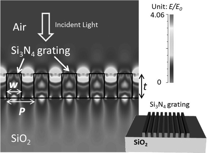
As shown in the inset picture of Fig. 1, the GMR grating consists of a thin layer of Si3N4 grating with thickness of t = 300 nm, which is deposited on a SiO2 substrate. The grating period is P = 340 nm and the grating width is w = 185 nm. Neglecting the material dispersion, the refractive indices of Si3N4 and SiO2 are 2.03 and 1.461 at 532 nm wavelength, respectively. The electric field distribution of a normal incident transverse-magnetic (TM) wave at 532 nm wavelength is calculated by rigorous coupled wave analysis (RCWA) method.15 The maximum electric field is 4-times the intensity of the incident light and concentrates in the upper area of the air gaps between the Si3N4 waveguides.
Figure 1.
Schematic of the proposed GMR grating and the simulated TM mode electric field distribution at the 532 nm resonant wavelength.
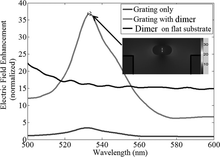
To investigate how the resonant mode interacts with metallic LSPPs, we use the RF module from COMSOL 3.5a to numerically compare different SERS substrates. A surface normal constant wave (CW) laser with 2 μm Gaussian width is used as the excitation light. The first SERS substrate is based on a GMR grating with the aforementioned parameters but without any metallic nanoparticles. We choose the maximum electric field point as the monitoring site. For the second SERS substrate, we use a flat Si3N4 substrate and place a silver nanoparticle dimer on top of it. The diameter of the silver particles is 25 nm and the gap between them is 1 nm. The maximum electric field is in the center of the gap. The last SERS substrate is designed by placing the same silver nanoparticle dimer on top of the GMR grating with the lower surface of the dimer aligned to the top surface of the Si3N4 waveguides. This position configuration is very similar to our experimental setup with SiO2 nanotubes being placed on top of the GMR grating. However, there is a misalignment between the peak electric field positions of these two structures due to geometric conflict. Again, the maximum electric field is found to be in the gap of the dimer. Fig. 2 shows the electric field enhancement (E/E0, where E0 is the peak electric field of the incident light) as a function of wavelength for the three SERS substrates. The enlarged view of the electric field distribution of the silver dimer on top of the GMR grating is shown in the inset picture as well. The peak EFs are found to be 35.
Figure 2.
Electric field enhancement of different SERS substrate at the wavelength range from 500-600 nm.
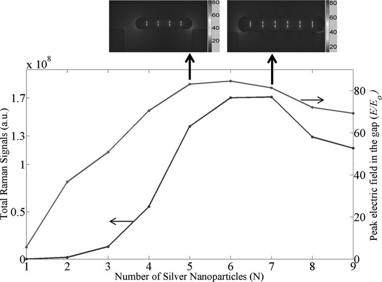
The effect of the distribution and the number of nanoparticles to SERS EFs on a flat substrate has been investigated.16, 17 However, the actual interaction between the LSPP and the GMR modes and the impact to SERS EFs are not reported yet. Comparing with nanoparticles on a flat substrate, the electric field enhancement of nanoparticles on GMR grating is more complex. On one hand, having more plasmonic nanoparticles on the grating not only creates more “hot spots,” but also enhances the LSPPs due to the near field coupled plasmon resonance of the chain,18 which results in the enhancement of the total Raman signals. On the other hand, plasmonic nanoparticles can absorb photon energy and damp the coupling between the LSPP and the GMR modes, which is detrimental to SERS signals. In this paper, we quantitatively investigate interactions between these two optical modes via numerical simulation, which can guide our experimental research. Our simulation is based on a simplified model of one-dimensional silver nanoparticle chain assembled on the surface of the GMR grating, and the SERE EF is calculated based on the well-known electromagnetic model: the SERS enhancement is proportional to |E|4.6 We need to consider two extreme cases for the actual SERS measurement. In the first case, the molecule concentration is extremely low. Within the laser spot, there is only one molecule and multiple hot spots. Hence, the SERS EFs are determined by the electric field in a single hot spot assuming that the molecule can be trapped in that specific gap. In the second case, the molecule concentration is relatively high. Within the laser spot, there are multiple hot spots and each hot spot has attracted one molecule. Therefore the total SERS signals are determined by 4, where Ei is the electric field in each hot spot. Assuming that we can collect all the Raman signals from every hot spot, we are actually using the total Raman signals to evaluate the SERS substrate. We plot both the peak electric field in the gap (corresponding to the first case) and the total Raman signals (corresponding to the second case) with respect to the number of silver nanoparticles as shown in Fig. 3, which indicates that there is an optimal number for the silver nanoparticles which can provide the strongest SERS signals. We can see that as the number of nanoparticles increases from 1 to the optimal number (for maximum electric field, the optimal number is 6; and for maximum Raman signals, the optimal number is 7), both the peak electric field and the total Raman signals increase. For example, E/E0 increases from 35 for a dimer with 2 silver nanoparticles to 80 for an array with 6 silver nanoparticles. One key point here is that the electric field distribution in the gaps of the nanoparticle chain is not uniform. The central gap has higher electric field than the edged gaps, as the top inset pictures of Fig. 3 show. This simulation results agree with those for silver nanoparticles in free space.18 In the meanwhile, adding more nanoparticles will create more hot spots, and the total SERS signals will increase even faster than |E|4. However, after reaching the optimal number of 6, the electric field starts to decrease. Although the number of hot spots keeps increasing, the total Raman signals quickly starts to drop as it is proportional to |E|4.
Figure 3.
Total Raman signals and peak electric field in the gap as a function of the number of the nanoparticle.
Two major fabrication steps are required for the designed SERS substrate. The SiO2 nanotubes with densely assembled silver nanoparticles are fabricated via rational chemical synthesis and the process is briefly discussed here. First, silver nanowires with controlled diameters and lengths are fabricated via electro-deposition into nanoporous templates;19 Second, the nanowires are used as templates for the synthesis of SiO2 nanotubes; Then, a layer of SiO2 with controlled thickness is uniformly coated on the outside surface of the nanowires; Next, the silver segments are selectively etched by nitric acid (8M), resulting in the hollow SiO2 nanotubes; Finally, a large amount of silver nanoparticles are uniformly synthesized on the entire surface of the SiO2 nanotubes with controlled sizes and gaps for SERS sensing. Detailed fabrication procedures of the plasmonic-active SiO2 nanotubes will be given in Ref. 20. These nanotubes are inspected by scanning electron microscopy (SEM). On the outer surface of the nanotubes, high density silver nanoparticles are found to be uniformly coated as shown in Fig. 4a. The SiO2 nanotubes have average diameters of 450 nm and lengths of 8 μm. The silver nanoparticles are semi-spherical with diameters of 24.9 ± 7.7 nm, and the mean gap sizes between the neighboring nanoparticles are controlled to be less than 1 nm. Although the nanoparticles are densely arranged, overlap among nanoparticles is rarely found. As a result, the entire surfaces of the nanotubes are active for SERS sensing due to the large amount of “hot spots” from the densely arranged silver nanoparticles. In the next step, we fabricate the GMR Si3N4 grating by e-beam lithography and ion etching. A 300 nm silicon nitride layer is grown by low pressure chemical vapor deposition (LPCVD) on a 1.5 μm field silicon oxide layer on top of a silicon wafer. The pattern of the GMR grating is written by e-beam photolithography. Then a 20 nm thick nickel layer is deposited by evaporation, and followed by a lift-off process. The nickel pattern is used as a hard mask to etch the nitride layer down to the buried oxide by reactive ion etching (RIE). Finally, the nickel residue is removed by chemical wet etching. Fig. 4b shows the SEM picture of the fabricated Si3N4 grating.
Figure 4.
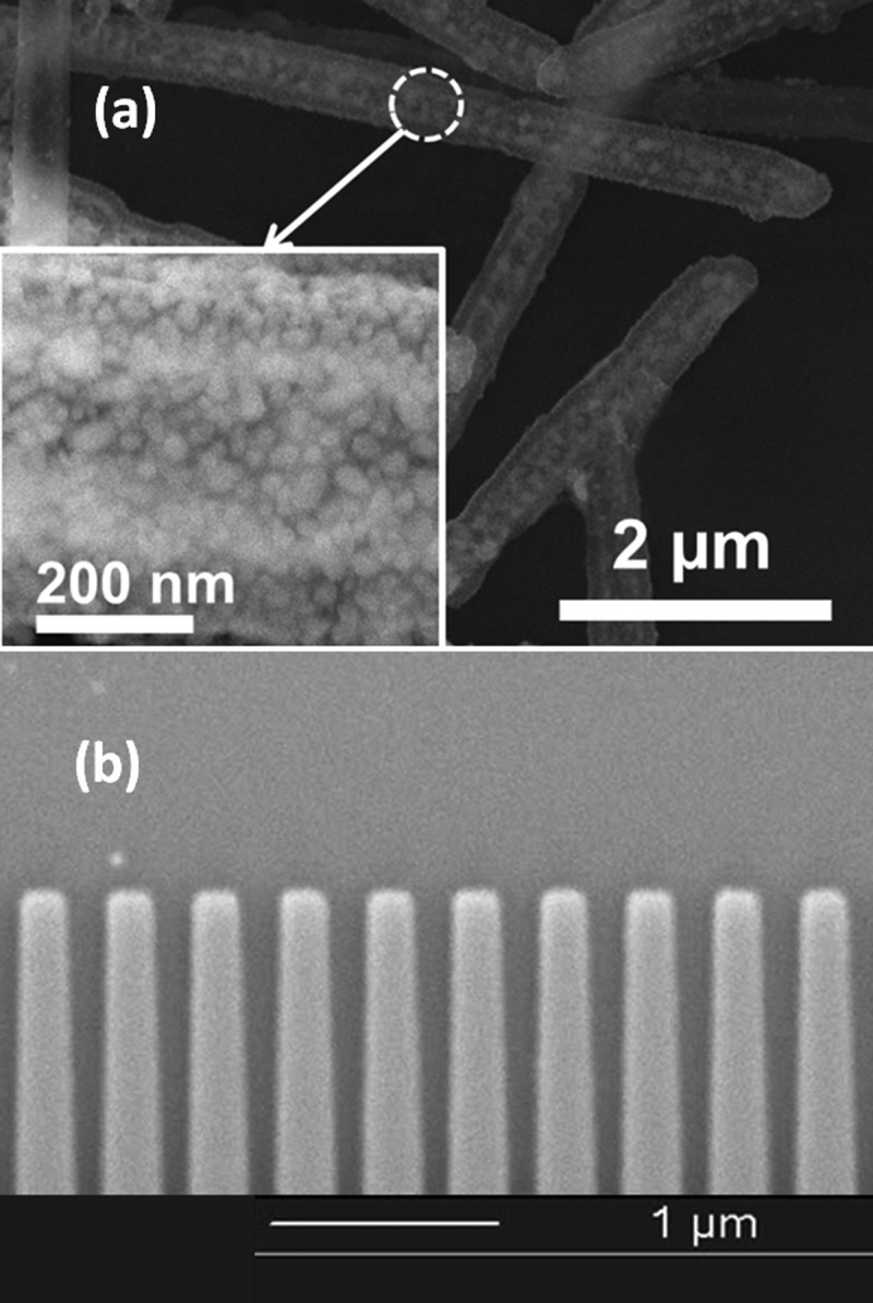
(a) SEM picture of the plasmonic-active SiO2 nanotubes with densely assembled silver nanoparticles. (b) SEM picture of the Si3N4 GMR grating.
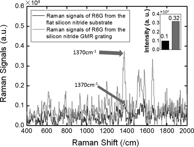
Rhodamine 6G (R6G), a standard SERS characterization dye, is selected as the detection probe. In the first experiment, we only use the GMR grating (without any plasmonic nanotube) to evaluate the grating effect. The R6G molecules are dispersed in ethanol with a very high concentration of 5 mM. A confocal Raman microscope equipped with a 532 nm laser is used for Raman spectroscopy measurement. The integration time is set at 1 s. Raman signals of 5 mM R6G from the flat Si3N4 substrate (blue) and the Si3N4 GMR grating (green) are plotted in Fig. 5. Although the measured Raman spectrums are quite noisy due to the extremely weak signals, the peak Raman shift at 1370 cm−1 is enhanced by 3.2 times, which clearly proves the electric field enhancement of the GMR grating.
Figure 5.
Measured 5 mM R6G Raman spectrum from the flat Si3N4 substrate and from the Si3N4 GMR grating (no plasmonic nanotubes for both cases).
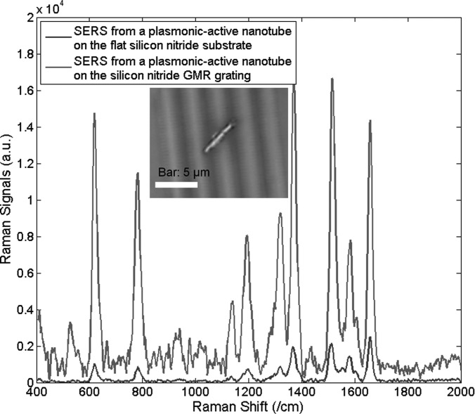
In the second testing, we include the plasmonic-active SiO2 nanotubes for SERS characterization. The R6G concentration is reduced to 1 μM, which can still form a monolayer that has enough concentration for molecule trapping in every hot spot. The laser spot size is 2 μm, which can be focused on any specific position of a single nanotube along its longitudinal direction. Within the laser spots, there are approximated 1000 hot spots that can contribute to Raman sensing. In each measurement, there is only one plasmonic-active SiO2 nanotube within the range of the laser spot. Fig. 6 shows the measured 1 μM R6G SERS signals from a SiO2 nanotube on the flat Si3N4 substrate (blue) and from a SiO2 nanotube on the Si3N4 GMR grating (green), respectively. The inset picture shows the 1000× optical microscope image of the Si3N4 grating with sparsely dispersed plasmonic-active SiO2 nanotubes. For various signature Raman shift peaks between 500/cm−1 to 1800/cm−1, the absolute intensity of the Raman signals is simultaneously enhanced by 8 ∼ 10 times. Since GMR grating increases the local electric field of the excitation light, it is not surprising to find that the noise signals that contain fluorescence and Raman spectra of various trace amounts of chemicals also increase with the electric field,21 and thus be amplified. Here, we note that the noise from fluorescence is proportional to E2 and the noise from Raman signals is approximately proportional to E4. As a result, both Raman signals from R6G and their noises can be enhanced by the GMR grating. Also, our further characterization shows that EFs are constant and stable across the whole surface of the plasmonic-active SiO2 nanotube. The absolute SERS EFs from the combined GMR grating and SiO2 nanotubes are majorly determined by the plasmonic enhancement from the nanoparticles, which can be tuned by their diameters and gap sizes, as the LSPPs can provide a much stronger electric field enhancement than the GMR grating does.20 The interesting phenomenon we observe here is that the GMR grating can provide 3.2× EFs on a pure dielectric substrate as shown in Fig. 5, while 8 ∼ 10× SERS EFs with plasmonic nanotubes in Fig. 6. This difference is possibly due to the measurement errors of extremely weak Raman signals without plasmonic nanotubes.
Figure 6.
Measured 1 μM R6G Raman spectrum from the SiO2 nanotube on the flat Si3N4 substrate and from the SiO2 nanotube on the GMR grating.
In conclusion, we have numerically investigated and experimentally demonstrated a SERS substrate comprised of Si3N4 GMR grating with plasmonic-active SiO2 nanotubes, where densely grown silver nanoparticles provide a large number of “hot spots” for SERS sensing. Such rationally designed SiO2 nanotubes can deliver an optimal amount of metallic nanoparticles to the Si3N4 grating to achieve sufficient LSPPs without significantly damping the GMR modes. Experimental measurement of R6G confirms that the SERS substrate can provide a constant and stable EFs of 8 ∼ 10 across the entire nanotube surface in addition to the existing SERS effect. As a new enhancement mechanism to SERS technology, the GMR grating coupled surface plasmonic resonance (SPR)-active nanotubes demonstrated in this paper proves that resonant photonic devices can indeed serve as an effective substrate to increase the sensitivity of Raman spectroscopy. Such highly sensitive SERS substrate will have significant potentials in early disease diagnostics, chemical detection and environmental protection.22, 23
Acknowledgments
The authors would like to acknowledge the support from the National Institutes of Health (NIH) under the Small Business Technology Transfer Research (STTR) program (Grant No. 1R41EB012885-01), Welch Foundation F-1734, China Scholarship Council, and the Faculty Startup Support from the School of EECS at Oregon State University.
References
- Jeanmaire D. L. and Van Duyne R. P., J. Electroanal. Chem. 84, 1(1977). 10.1016/S0022-0728(77)80224-6 [DOI] [Google Scholar]
- Albrecht M. G. and Creighton J. A., J. Am. Chem. Soc. 99, 5215 (1977). 10.1021/ja00457a071 [DOI] [Google Scholar]
- Kneipp K., Wang Y., Kneipp H., Perelman L. T., Itzkan I., Dasari R., and Feld M. S., Phys. Rev. Lett. 78, 1667 (1997). 10.1103/PhysRevLett.78.1667 [DOI] [PubMed] [Google Scholar]
- Camden J. P., Dieringer J. A., Wang Y., Masiello D. J., Marks L. D., Schatz G. C., and Van Duyne R. P., J. Am. Chem. Soc. 130, 12616 (2008). 10.1021/ja8051427 [DOI] [PubMed] [Google Scholar]
- Qian X.-M. and Nie S. M., Chem. Soc. Rev. 37, 912 (2008). 10.1039/b708839f [DOI] [PubMed] [Google Scholar]
- Le Ru E. C., and Etchegoin P. G., Principles of Surface-enhanced Raman Spectroscopy (Elsevier, Oxford, UK, 2009). [Google Scholar]
- Kuncicky D. M., Prevo B. G., and Velev O. D., J. Mater. Chem. 16, 1207 (2006). 10.1039/b512734c [DOI] [Google Scholar]
- Banholzer M. J., Qin L., Millstone J. E., Osberg K. D., and Mirkin C. A., Nat. Protoc. 4, 838 (2009). 10.1038/nprot.2009.52 [DOI] [PMC free article] [PubMed] [Google Scholar]
- White I. M., Gohring J., and Fan X., Opt. Exp. 15, 17433 (2007). 10.1364/OE.15.017433 [DOI] [PMC free article] [PubMed] [Google Scholar]
- Jackson J. B., Westcott S. L., Hirsch L. R., West J. L., and Halas N. J., Appl. Phys. Lett. 82, 257 (2003). 10.1063/1.1534916 [DOI] [Google Scholar]
- Hu M., Fattal D., Li J., Li X., Li Z., and Williams R. S., Appl. Phys. A 105, 261 (2011). 10.1007/s00339-011-6613-8 [DOI] [Google Scholar]
- Li J., Fattal D., and Li Z., Appl. Phys. Lett. 94, 263114 (2009). 10.1063/1.3168498 [DOI] [Google Scholar]
- Kim S -M., Zhang W., and Cunningham B. T., Opt. Exp. 18, 4300 (2010). 10.1364/OE.18.004300 [DOI] [PubMed] [Google Scholar]
- Karagodsky V., Tran T., Wu M., and Chang-Hasnain C. J., in IEEE CLEO CFN1, Baltimore, MD, 2011.
- Moharam M. G. and Gaylord T. K., J. Opt. Soc. Am. 3, 1780 (1986). 10.1364/JOSAA.3.001780 [DOI] [Google Scholar]
- Fang Y., Seong N.-H, and Dlott D. D., Science 321, 388 (2008). 10.1126/science.1159499 [DOI] [PubMed] [Google Scholar]
- Margueritat J., Gehan H., Grand J., Levi G., Aubard J., Felidj N., Bouhelier A., Colas-Des-Francs G., Markey L., Marco De Lucas C., Dereux A., and Finot E., ACS Nano 5, 1630 (2011). 10.1021/nn103256t [DOI] [PubMed] [Google Scholar]
- Wang Z. B., Lukyanchuk B. S., Guo W., Edwardson S. P., Whitehead D. J., Li L., Liu Z., and Watkins K. G., J. Chem. Phys. 128, 094705 (2008). 10.1063/1.2835598 [DOI] [PubMed] [Google Scholar]
- Fan D. L., Zhu F. Q., Cammarata R. C., and Chien C. L., Nano Today 6, 339 (2011). 10.1016/j.nantod.2011.05.003 [DOI] [PMC free article] [PubMed] [Google Scholar]
- Xu X., Li H., Ruoff R., Wang A. X., and Fan D., “Rational synthesis of plasmonic-magnetic bifunctional nanotubes for biological applications” (unpublished).
- Weber M. L., Litz J. P., Masiello D. J., and Willets K. A., ACS Nano 6, 1839 (2012). 10.1021/nn205080q [DOI] [PubMed] [Google Scholar]
- Choo-Smith L.-P., Edwards H. G. M., Endtz P., Kros J. M., Heule F., Barr H., J. S.Robinson, Jr. , Bruining H. A., and Puppels G. J., Biopolymers 67, 1 (2002). 10.1002/bip.10064 [DOI] [PubMed] [Google Scholar]
- Vo-Dinh T., Yan F., and Wabuyele M. B., J. Raman Spectrosc. 36, 640 (2005). 10.1002/jrs.1348 [DOI] [Google Scholar]


