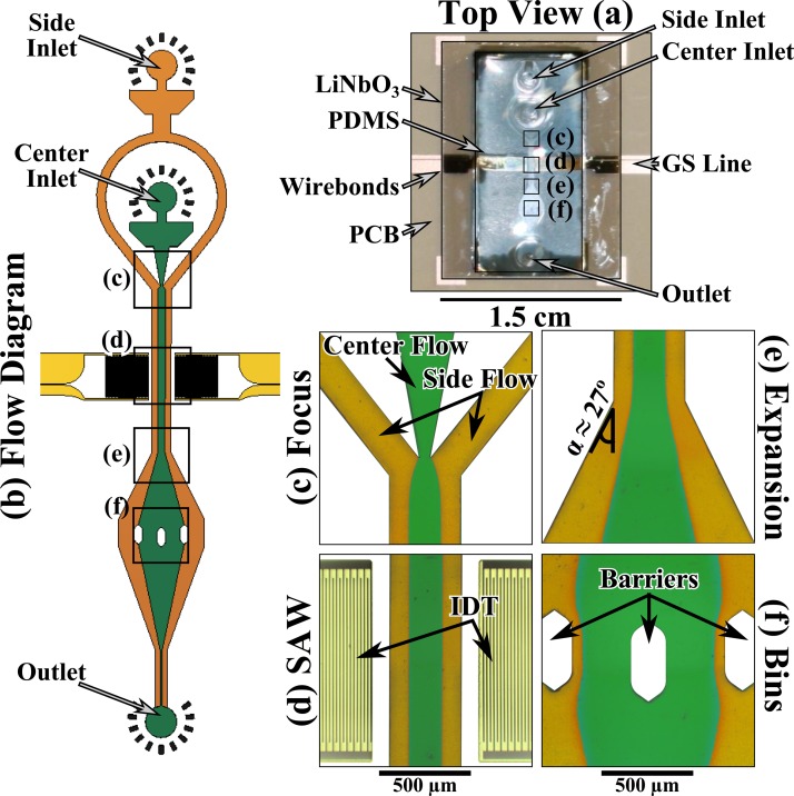
Figure 1.
(a) The integrated acoustic microfluidic device (about the size of a US 10¢ piece) mounted on a PCB. The PDMS microfluidic circuit was bonded to a double-side polished single crystal LiNbO3 chip. (b) The flow diagram of the microfluidics. (c) The flow focus that was used to focus the green buffer into the center of the channel and away from the side walls with yellow buffer. (d) The SAW region consists of two IDTs made from 750 nm of gold that were fed by ground-signal lines with a 91 MHz signal. The SAW was encased in an air void fabricated in the PDMS that also contains the microfluidics. (e) The 27° expansion region that was used to change the trajectory of the bead streams. (f) The binning region that consists of 3 barriers placed on an arc, creating four equally spaced bins. The panels (c)-(f) are digitally manipulated micrographs.

