Abstract
This paper describes the design of CMOS receiver electronics for monolithic integration with capacitive micromachined ultrasonic transducer (CMUT) arrays for high-frequency intravascular ultrasound imaging. A custom 8-inch wafer is fabricated in a 0.35 μm two-poly, four-metal CMOS process and then CMUT arrays are built on top of the application specific integrated circuits (ASICs) on the wafer. We discuss advantages of the single-chip CMUT-on-CMOS approach in terms of receive sensitivity and SNR. Low-noise and high-gain design of a transimpedance amplifier (TIA) optimized for a forward-looking volumetric-imaging CMUT array element is discussed as a challenging design example. Amplifier gain, bandwidth, dynamic range and power consumption trade-offs are discussed in detail. With minimized parasitics provided by the CMUT-on-CMOS approach, the optimized TIA design achieves a 90 fA/√Hz input referred current noise, which is less than the thermal-mechanical noise of the CMUT element. We show successful system operation with a pulse-echo measurement. Transducer noise-dominated detection in immersion is also demonstrated through output noise spectrum measurement of the integrated system at different CMUT bias voltages. A noise figure of 1.8 dB is obtained in the designed CMUT bandwidth of 10 MHz to 20 MHz.
Index Terms: Transimpedance, low-noise, input referred noise, capacitive sensor, current sensor, CMUT, monolithic, CMOS MEMS
I. Motivation for Monolithic Integration
Intravascular ultrasound (IVUS) imaging has emerged as a valuable tool for interventional cardiology to manage diseases of the coronary arteries [1, 2]. Capacitive micromachined ultrasonic transducers (CMUTs) have been shown to be a viable alternative to piezoelectric transducers for IVUS because they exhibit comparable performance, while allowing for easier fabrication of complex arrays and more compact electronics integration [3]. The silicon-micromachined CMUT is especially suitable for various levels of CMOS integration on a single substrate. The ability to integrate electronics is a key factor for successful implementation of catheter-based imaging arrays, especially for ring annular arrays [4, 5] and densely populated 2D arrays [6, 7] because the maximum number of cables is limited by the catheter diameter. Additionally, this application demands tight front-end electronics integration, as the typical element size is on the order of 100 μm implying a high sensitivity to parasitics associated with cables and wirebonds.
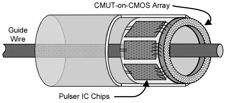
The specific application considered here is forward-looking (FL)-IVUS, a system that would be useful for dealing with chronic total occlusions (CTO) in blood vessels and guiding stent placements. A previous study for FL-IVUS using piezoelectric transducers is found in [8]. More recent studies relied on CMUT devices for FL- IVUS [4, 5, 9] because it is challenging to fabricate piezoelectric devices with the required dimensions. Fig. 1 shows the schematic diagram of a FL-IVUS probe with a CMUT array integrated with front-end receiver electronics.
Fig. 1.
Schematic diagram of a forward-looking IVUS catheter employing CMUT-on-CMOS. The receiver circuitry is monolithically integrated with the CMOS array on the tip of the catheter which minimizes the interconnect parasitics. Transmit circuitry chips may be separate and located on the sides.
The parasitic interconnect capacitance is a significant factor degrading the signal-to-noise ratio on the receive side of FL-IVUS array elements with very small capacitances [10]. A method for reducing electrical interconnect parasitics is through-wafer-via interconnect technology. Using flip-chip bonding to electronics, a total interconnect parasitic capacitance between 100 fF to 500 fF was reported [7]. This hybrid-integration approach allows circuits and CMUTs to be optimized separately; however it requires extra fabrication steps including flip-chip bonding, which increases complexity. Previous efforts of single-chip integration of CMOS and CMUT devices include [11] where a BiCMOS fabrication process with modified steps was used to build CMUTs during electronics fabrication. The main drawback of that approach is that it uses an intermediate CMOS micromachining process and thus alters standard electronics fabrication, which adds extra cost. In addition, transducer design is limited because this approach does not allow any control over gap or membrane thicknesses. One can also use conventional CMOS process flow without modifying the electronics fabrication to build CMUTs where the metal and passivation layers are etched during post-CMOS processing [12, 13]. In these approaches the CMUT design is still limited by the existing foundry procedure. In addition, CMUT elements have to be located on the side of the electronics, which is not acceptable for dense arrays.
A viable approach to mitigate parasitic interconnect capacitances relies on monolithic integration of CMUTs with CMOS electronics where sensor elements are formed on the same silicon substrate with the CMOS electronics [14, 15]. In this paper, we report a CMUT-on-CMOS approach where CMUT elements are built after the CMOS fabrication and both electronics and CMUT designs are separately optimized. The single chip CMUT-on-CMOS integration significantly reduces the interconnection complexity, increases compactness, enables a smaller die size and reduces cost.
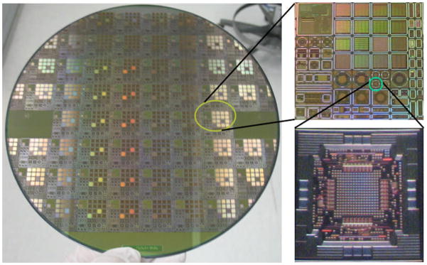
To implement the monolithic system, we designed a custom wafer in TSMC (Taiwan Semiconductor Manufacturing Co.) 0.35 μm two-poly, four-metal CMOS process and integrated CMUT arrays using a low-temperature fabrication process [16]. The 8-inch CMOS wafer contains many reticles of size 2 cm × 2 cm. Part of the reticle contains many smaller ASICs that are optimized to interface with various CMUT arrays having different bandwidths and geometries (Fig. 2).
Fig. 2.
The picture of the 8-inch CMOS wafer fabricated in a 0.35 μm CMOS (left), the picture of the 2 cm × 2 cm reticle (top right) and the 1.5 mm × 1.5 mm chip designed to interface with a forward-looking CMUT array (bottom right).
In this paper, we focus on an ASIC that is custom-designed to interface with a FL-IVUS CMUT array as the advantages of monolithic integration are more pronounced for this particular application. Fig. 3 depicts the monolithic integration scheme and the connection to the receiver array through the bottom electrode of the transducer. We describe the design of the full system IC and present a high-bandwidth, high-gain, low-noise transimpedance amplifier design that can achieve a noise performance comparable to the transducer noise limit due to the reduced interconnection capacitance provided by the monolithic CMUT-on-CMOS approach.
Fig. 3.

The receive amplifier is connected to the bottom electrode. CMUT is biased with a high voltage DC on the top electrode. Not shown in this figure is an oxide passivation layer between the CMUT bottom electrode and the CMOS ASIC.
II. Choice of Preamplifier
The motion of the CMUT membrane due to the received ultrasound pressure modulates the sensor capacitance. This generates a current signal that can be expressed as
| (1) |
where VBIAS is the voltage applied to one of the CMUT electrodes that biases the device close to the collapse voltage, C0 and d0 are the static capacitance and the gap distance, respectively, and δd/δt is the velocity of the membrane. Since the CMUT current signal is proportional to the velocity of the membrane, which is directly related to the wideband pressure input, the preamplifier should perform wideband current amplification in order not to limit the sensor signal bandwidth. Therefore, wide bandwidth current amplification using a transimpedance amplifier (TIA) was deemed to be a viable approach for the velocity sensor [17].
A common-source voltage amplifier [18], a two stage voltage amplifier [19] or a continuous time charge amplifier [12, 15, 20] would be suitable for voltage sensing, and when used as a CMUT preamplifier would limit the bandwidth. CMUT voltage is the integrated version of the wideband CMUT current signal and therefore to prevent limiting the CMUT bandwidth a differentiator circuit should follow the voltage sensors [21, 22], which introduces an additional stage in the receiver chain.
The TIA has a low input impedance which is desirable to maximize the received current signal, but not suitable for electrical impedance matching. Electrical impedance matching at the receiver is needed to reduce reflections of the incoming acoustic energy back to the medium [23]. For small array elements multiple reflections are not large enough to create imaging artifacts. Therefore, to maximize the received current signal we implemented a low input impedance transimpedance amplifier with a common-source core stage with shunt feedback for wideband and low-noise performance.
III. Front End ASIC For Dual Ring Array
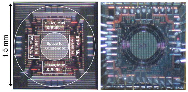
Fig. 4-left shows a micrograph of an ASIC that is designed to interface with an 800 μm diameter FL dual-ring CMUT array, which includes two rings of CMUT elements [5]. The inner ring includes 24 elements for transmitting ultrasound and there are 32 elements on the outer ring for receiving the acoustic signal. The post processed IC with the monolithically integrated CMUT array is shown in Fig. 4-right. Array elements are designed with an electrode area of 70 μm × 70 μm. The vacuum gap is 0.12 μm and the thickness of the nitride isolation layers is 0.2 μm. The operation frequency in immersion is between 10 MHz and 20 MHz.
Fig. 4.
The micrograph of the designed ASIC (left) and the same chip after CMUT post-fabrication (right).
A dedicated low-noise transistor-feedback transimpedance amplifier is provided for each of the 32 receiver elements. The chip includes 4 sets of receiver circuitry, each containing 8 amplifiers. Multiplexing is required for low cable count, which is essential for catheter applications. Therefore each set of the receiver circuitry contains one 8×1 multiplexer. The chip has a total of 4 outputs, one from each receiver array. The operating supply voltage is 3.3 V.
Each receiver set contains a buffer to drive the interconnect cable and scope capacitances, each on the order of 10 pF. We use a push-pull buffer including two source follower stages. In order to not limit the signal bandwidths, the buffer is designed to have a wide bandwidth that is higher than 50 MHz with 50 Ω resistive or highly capacitive loads. With a 50 Ω load, the gain of the buffer stage is around 0.25 V/V. For noise measurements, the buffer output is loaded with the 50 Ω input impedance of the spectrum analyzer so the measured buffer output noise values are reflected to the receive amplifier output by dividing by 0.25. With capacitive loads, the gain of the buffer is around 0.6. The buffer consumes 1 mA of current and covers an area of 35 μm × 50 μm.
The ASIC in Fig. 4 fits in a 1.5 mm diameter circular area including all the bondpads. A 500 μm diameter circle at the center is reserved for the guide-wire. There are a total of twelve pins: Four outputs on four sides, one TIA gain tuning voltage, three multiplexer selects, a TIA core amplifier bias, two vdd pins for better power routing and a ground. Additional pads on the CMUT post-fabricated chip are for the two CMUT DC biases for the receive and transmit rings and 24 of the connections are for the transmit elements. High voltage transmit pulses are provided externally through those pads. Many small squares seen on the chip micrograph are stacked metal layers that are included for metal fill to meet CMOS density rules and there is no active circuitry under those metal fills. Inputs of the amplifiers are connected to the highest metal (metal 4) that is 15 μm wide. An initial patterning step on the CMOS ASIC is used to create small openings in the passivation layer over these metal 4 amplifier input pads. During the subsequent CMUT fabrication, the bottom electrodes of the receive CMUT elements coat these openings and create an electrical connection to the CMOS amplifiers below.
Fig. 1 shows the pulser chips on the side of the catheter tip that requires many interconnects between the pulser chips and the CMUT array. Considering the space constraints for the forward-looking array element, and the ease of packaging, in the next generation design the pulser circuitry can be combined with the receiver electronics in a single IC. High-voltage pulsers in a low-voltage technology can be designed by modifying the layout of the regular devices from a low voltage process [24]. This is a low cost solution because it doesn’t require any additional fabrication steps.
The layout of the preamplifier TIA used in the ASIC is 70 × 140 μm2, which is equal to the total area of one transmit-receive pair of CMUT elements so that the receiver circuitry fits under the footprint of the CMUT array. Each TIA consumes 2 mA of current and 32 elements consume a total of 64 mA of current from a 3.3 V supply, which exceeds the 100 mW power budget noted in [25] for intravascular ASICs. Although in this current design all receiver amplifiers consume power, at any time only four of them are connected to the output. To reduce the power consumption some intelligence can be added to the future ASICs and the amplifiers that are not actively used can be switched off. With this method only four amplifiers consume power and the rest stay inactive. Hence, power consumption can be reduced to 1/8th of its current values, well below the 100 mW limit even with 64 receivers.
A. Wideband Pulse Echo
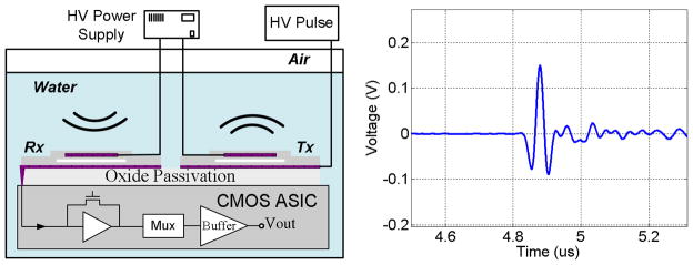
We performed pulse-echo experiments in water to verify the functionality of the monolithically integrated CMUT array. The setup for the ultrasonic measurement is illustrated in Fig. 5-left. The top electrode of the receiver array is common to all of the elements and the high voltage dc bias is applied to this common top electrode. The receiver element is biased at its top electrode to about 80% of the collapse voltage and the bottom electrode (the electrode closest to the CMOS electronics) is connected to the TIA through the topmost metal layer. The receiver transimpedance amplifier dc input voltage is around 1 V and is much smaller than the dc bias that is applied from the top electrode. The CMUT itself acts as a capacitive block between the high voltage bias and the receive circuitry. All transmit elements also share a single DC bias through a connection to their common top electrode. The bottom electrodes of the transmit elements are connected to external pads to route TX pulses to the CMUT elements. The oxide passivation layer between the CMUT bottom electrode and the ASIC top metal level protects the ASIC from the high voltage pulse.
Fig. 5.
The test setup (left) and the measured pulse-echo response from the monolithically integrated array from the water air interface (right).
The CMUT-CMOS chip was wirebonded on a 40-pin package for testing and the connections were coated with parylene to prevent electrical shorting. One CMUT element from the inner ring was used as a transmitter and an element from the outer ring was used as a receiver. A narrow pulse was applied to the bottom electrode of the transmit element. Fig. 5-right shows the echo signal from a planar water-air interface, with a center frequency of 15.2 MHz. The tail in the echo response is mainly due to the acoustic crosstalk and the ringing in the silicon substrate [3]. This basic experiment shows that the monolithically integrated system is fully functional.
IV. Noise Optimization Enhanced by Monolithic Integration
Optimization of the signal-to-noise ratio (SNR) of the transducer system requires designing receiving electronics that introduce the lowest possible noise for the given bandwidth and element size. The FL-CMUT array elements are particularly small and the use of synthetic aperture data acquisition limits the available signal levels. This makes the minimization of the input-referred electronic noise a critical task. Ideally the system noise should be limited by the CMUT thermal-mechanical noise, which is shaped by the CMUT electrical impedance. Due to its small size, the FL-CMUT element generates very low thermal-mechanical noise making it challenging to design a transducer noise limited front end receiver.
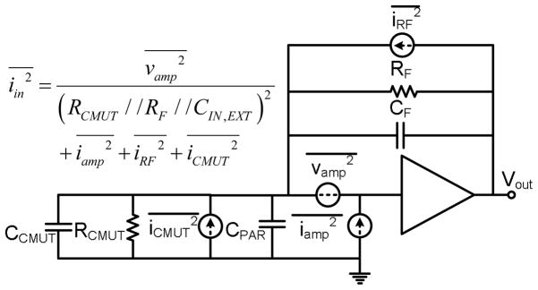
A schematic of the noise sources including the CMUT element and the receiving TIA is shown in Fig. 7. A CMUT element in immersion can be simply modeled as a parallel resistor and a capacitor [26]. Therefore the CMUT element is represented with a capacitor and an AC equivalent resistor. The CMUT impedance introduces a thermal-mechanical noise to the system that is shown as [27]. Using the transducer design parameters, when biased close to collapse, the FL-CMUT element capacitance and resistance are calculated to be 150 fF and 1 MΩ, respectively.
Fig. 7.
The schematic of the system noise components including the electronics noise and the CMUT thermal-mechanical noise (iCMUT2) and the expression for the total input referred current noise (iin2). CIN,EXT is the sum of the capacitances external to the core amplifier and includes CF, CPAR, and CCMUT.
As discussed in section II, the CMUT output is a current and therefore the input referred current noise of the front end is of interest. For this design, the total input referred current noise is given by:
| (2) |
where CIN, EXT is the sum of the capacitances external to the core amplifier, including the CMUT capacitance, the parasitic capacitance at the input (CPAR) and the feedback capacitance (CF). represents the thermal noise of the feedback resistor (RF). and are the input equivalent current and voltage noise sources of the core amplifier that can be expressed as
| (3) |
where gm is the transconductance, CIN,AMP is the capacitance, and id2 is the current noise of the input transistor that dominates the core amplifier noise. The total input referred current noise expression including all the capacitances connected to the input can then be expressed as [28]
| (4) |
Inspecting (4), it can be seen that the core amplifier related noise increases with frequency and the rate of increase is proportional to the total capacitance at the input. If the receive sensor element is connected to the amplifier using wirebonding, the parasitic bondpad and wirebond capacitances increase the total input capacitance degrading the noise performance significantly. This effect is more detrimental for small-sized FL-CMUT array elements. Monolithic integration removes all the wirebonding and pad capacitances at the input and results in better noise performance. In addition, as discussed in the next chapter, with reduced total input capacitance, RF can be designed with values much higher than is possible with wirebonding, which also reduces the input referred noise.
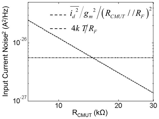
Fig. 8 is plotted to investigate the effect of RCMUT on the input referred amplifier noise. Values of two noise terms in (4), namely and 4k T/RF are calculated with respect to RCMUT. For this plot RF is assumed to be 3 MΩ and is assumed to be (1.1 nV/√Hz)2 based on the simulation values. Plot shows that for RCMUT values higher than 20 kΩ, the 4k T/RF term dominates the term. For FL array elements, RCMUT is calculated to be around 1 MΩ in immersion. Therefore, in this application, the term can be safely neglected in the total input referred amplifier noise expression in (4).
Fig. 8.
The two noise terms in (4) with respect to RCMUT. The y-scale is drawn in log scale. This plot shows that for higher RCMUT values the total noise does not depend on the CMUT equivalent resistance.
V. Transistor Feedback TIA Design and Core Amplifier Characteristics
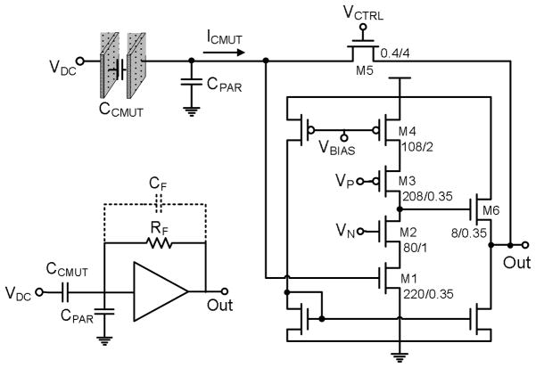
The schematics for the resistor feedback TIA and its full transistor implementation in this work are shown in Fig. 9. The gain of the transimpedance amplifier is set by the feedback resistance (RF). Since larger RF not only increases the sensitivity of the front-end but also minimizes the noise, a straightforward design approach is to maximize the value of RF for a given CMUT capacitance while maintaining adequate small signal bandwidth.
Fig. 9.
The resistor feedback TIA (left bottom) and the full transistor implementation (right). Transistor dimensions are given in μm’s. Parasitic interconnect capacitance (CPAR) limits the gain of the receiver and increases noise. Monolithic integration improves performance by minimizing CPAR.
With a finite bandwidth core amplifier, The TIA transfer function has two poles and is a second order system. The transfer function of the transimpedance amplifier can be given as
| (5) |
For a complete analysis, this quadratic system should be studied separately for two cases. The first case is without a feedback capacitor and the second case is with a feedback capacitor. Considering the first case and therefore assuming a zero value of CF, the design equations in (5) can be written as
| (6) |
In these equations wo and Ao are the bandwidth and gain of the core amplifier, respectively. CIN is the total capacitance at the input and includes the input capacitance of the core amplifier, the CMUT capacitance (CCMUT) and the interconnect parasitics (CPAR). For critical damping and a maximally flat 2nd-order Butterworth frequency response, Q should be set to √2/2. With critical damping, the 3dB bandwidth of the TIA is equal to its resonance frequency, wN. Assuming wIN is much smaller than w0, it can be found that for critical damping, the 3dB bandwidth of the core amplifier must be √2 times the closed-loop bandwidth of the TIA [29]:
| (7) |
On the other hand, if there is considerable CF, for high values of RF, the second order response is dominated by the pole due to the RF and CF , and in that case the bandwidth of the closed-loop response can be estimated by [7, 17]
| (8) |
For some TIA applications using discrete op-amps, the op-amps are often not designed specifically for the TIA implementation and for those cases a capacitor in feedback (CF) with an optimized value is used for stable closed-loop operation [30]. On the other hand, for custom designed TIA’s, the core amplifier gain and bandwidth can be designed to eliminate the need for an additional stability compensation feedback capacitance. Therefore for custom designs this shunt capacitance across the feedback is considered as a parasitic capacitance because large values of CF have a substantial effect on the bandwidth of the TIA and significantly limits the maximum value of RF that can be implemented. For instance, considering (8) a 50 fF feedback capacitance allows only a 160 kΩ of RF value for a 20 MHz closed-loop bandwidth. Therefore to maximize the RF value, the parasitic CF should be minimized.
A. Discussion of Trade-offs and Design Choices
TIA designs that implement the feedback resistance with a passive resistor [7] suffer from high values of CF due to the parasitic capacitances associated with the large area of the polysilicon resistors. In our TIA design, the feedback resistance is implemented using a single long-channel NMOS transistor (M5) in the triode region instead of a polysilicon resistor (Fig. 9). The effective resistance value of the triode region feedback transistor is approximated by:
| (9) |
where μN is the carrier mobility, COX is the gate capacitance per unit area, W is the channel width, L is the channel length and VT is the threshold voltage of the transistor. VCTRL is the control voltage to tune the closed-loop gain of the TIA. The aspect ratio for M5 is chosen to be W/L = 0.4μm/4μm.
A transistor covers much less area than an equal value on chip resistor, which significantly reduces the layout real estate and reduces the parasitic feedback effects. With careful layout practices such as keeping the input and output traces far from each other on the layout, the parasitic feedback capacitance can be eliminated. In that case, the design equations (6) and (7) that assume no feedback capacitance should be used. In (7) the w−3dB expression indicates a direct trade-off between the input capacitance (CIN) and the maximum RF value that can be implemented. Therefore any parasitic capacitance at the input should be minimized as it degrades the allowable RF value. Monolithic integration eliminates this parasitic capacitance and hence enables the use of a higher RF value.
Based on (7), the core amplifier bandwidth should be tuned to be around 30 MHz to get a desired closed-loop TIA bandwidth around 20 MHz. Also, it can be seen that the gain of the core amplifier should be maximized to obtain the highest RF and highest sensitivity. In this work to have a high gain, the core amplifier is designed as a cascoded common-source amplifier (Fig. 9) and has a simulated open loop gain of 180 when the open loop bandwidth is tuned to 30 MHz. The sizings of the transistors are also noted in Fig. 9. The bias current to the core amplifier is controlled with an external connection (VBIAS). The cascode transistor biasing (VP, VN) are provided through the on-chip biasing circuitry.
The core amplifier related noise given in (4) is proportional to the voltage noise ( ) term, which is inversely proportional with the transconductance (gm). To get a higher gm for a given current value, an NMOS (M1) is used at the input instead of a PMOS device. Increasing the bias current increases gm and hence reduces the voltage noise term. This creates a trade-off between the power consumption and the part of the noise increasing with frequency. Since the objective of this work is to minimize noise as much as possible, the bias current through M1 is designed to be close to a relatively high value of 2 mA. The cascode transistors are designed with a high W/L ratio to increase the gain of the core amplifier and to keep the transistors in saturation. The W/L ratio of M1 was designed to a high value of 220μm/0.35μm to increase gm. Simulated transconductance (gm) of the input transistor is 23 mS. The equivalent noise voltage of the core amplifier (vamp) is simulated to be about 1.1 nV/√Hz. The simulated input capacitance for the core amplifier (CIN,AMP) is around 400 fF.
VI. Gain and Noise Measurement Results
A. Transfer Function Testing
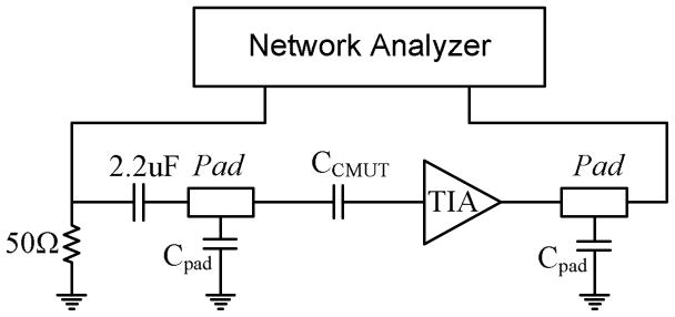
Testing the frequency response of a transimpedance amplifier is not a trivial task. One way of imitating a current source at the input is to use a large on-chip resistor [31]. The simulated input impedance of the designed TIA for a 3 MΩ feedback resistance is found to be 16.5 kΩ. Therefore, for accurate testing, the on-chip resistor should have a resistance much higher than 16.5 kΩ. However, a high value on-chip resistor consumes considerable layout area which results in parasitic capacitances which may affect the bandwidth characteristics of the TIA. Therefore we used an alternative method to measure the transimpedance characteristics, and used the CMUT element itself in series with the TIA to mimic the on-chip high impedance. The test setup can be seen in Fig. 10. A voltage signal is applied to the biasing electrode of the CMUT array. The Norton equivalent of a voltage input (Vin) in series with the CCMUT is a current source equal to Vin*2π* freq * CCMUT and a parallel CCMUT. Therefore the effect of the capacitance of the CMUT at the TIA input is also included in this measurement. This setup does not take into account the increase in the CMUT capacitance when a DC bias is applied to the CMUT element. However, for this small CMUT element a 50 fF capacitance increase is almost negligible because it is an order of magnitude smaller compared to the total capacitance at the TIA input. This test structure is also verified in simulation where a voltage source is connected in series with the CMUT capacitance and an ideal integrator is placed after the TIA output voltage. This simulation setup gives the same transimpedance characteristics when compared to the results of the simulation of the TIA with an ideal current source at the input.
Fig. 10.
Setup for testing the TIA transimpedance characteristics. The pad capacitance, Cpad, does not have an effect on the measured transimpedance because the CCMUT is located after the pad.
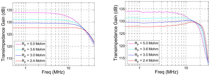
The simulated transimpedance characteristics for different values of feedback resistance are shown in Fig. 11-left. To be consistent with the electrical measurement, which is discussed next, a 100 fF capacitance is used in simulation to mimic the CCMUT. In simulations, there is a 0.3 fF drain-to-source capacitance that is included in the simulation model of the feedback transistor (M5) and it behaves as a feedback capacitor. However, its size is very small and does not impose a substantial damping. In addition, this capacitance is for transistor modeling purposes only and is not a physical capacitance. In the layout of the TIA, the metal connections are routed carefully not to introduce capacitance between the input and output of the amplifier. So, in the real implementation, the effective CF should be almost zero.
Fig. 11.
The transimpedance gain characterization with simulation (left) and electrical measurement (right). Both measurement and simulation results demonstrate that the bandwidth is higher than 20 MHz for a 3 MΩ transimpedance gain.
For electrical measurements, one of the outputs of the post processed IC in Fig. 4 is connected to an Agilent 4395A and the gain is measured at the buffer output using the equipment in network analyzer mode. Then the measured voltage gain is divided by the buffer gain and multiplied by 1/2π* freq * CCMUT to extract the transimpedance gain. Since the dc bias between the CMUT electrodes is very small for this test setup, to extract the TIA gain from the overall voltage gain measurement, a 100 fF is used as the CMUT capacitance. The transimpedance gain is characterized for different values of feedback resistance and plotted in Fig. 11-right. It can be seen from both the simulation and measurement results that the feedback resistance can be tuned by the control voltage. For increased transimpedance gains, the bandwidth of the TIA drops as expected. Measurement results demonstrate that a 3 MΩ gain can be achieved with a bandwidth higher than 20 MHz. This performance is also supported by the simulation results.
In simulations, when the core amplifier has a 30 MHz open loop bandwidth, even a feedback capacitance as low as 5 fF significantly damps the circuit and reduces the closed-loop bandwidth. The measured results in Fig. 11-right agree well with the simulations where the only feedback capacitance comes from the very small 0.3 fF from the transistor model. Therefore it can be stated that even if there is an unexpected CF due to parasitics, the measurement results suggest that it is much lower than 5 fF.
B. Noise Measurements
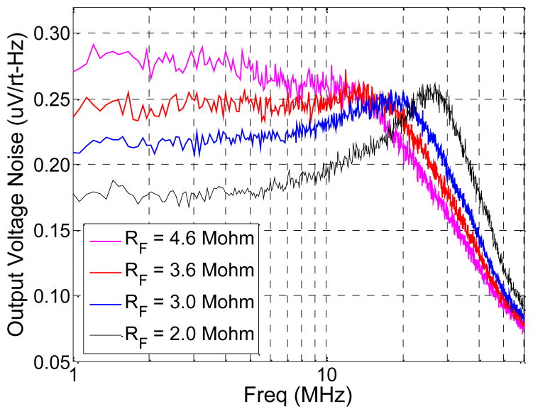
For noise measurement of the TIA, one of the outputs of the post processed IC in Fig. 4 is connected to an Agilent 4395A in spectrum analyzer mode. No bias is applied to the receiver CMUT to only measure the front end electronics noise. The output noise value of the TIA is obtained by dividing the measured output noise value by the buffer gain. Fig. 12 plots the measured output voltage noise of the TIA for different values of Vctrl. Each noise level at low frequencies corresponds to the thermal noise of the respective tuned RF value and is equal to . Therefore gain information of the transimpedance amplifier can be extracted from the flat region of the output noise spectrum. The plot clearly depicts the change in the TIA output noise spectrum with changing feedback resistance. At higher frequencies the TIA output noise starts to roll off, which is governed by the TIA transfer function. It can be seen that for the RF = 3 MΩ case, the output noise does not start to roll off until 20 MHz. This observation supports the TIA gain measurements demonstrating a 3 MΩ gain with a bandwidth higher than 20 MHz.
Fig. 12.
The output voltage noise of the TIA that is monolithically integrated to a forward-looking CMUT element with various feedback resistance values. For higher feedback resistances the output noise starts to roll off at smaller frequencies as the TIA bandwidth reduces. The noise plot for the 3 MΩ RF does not start to roll off until 20 MHz.
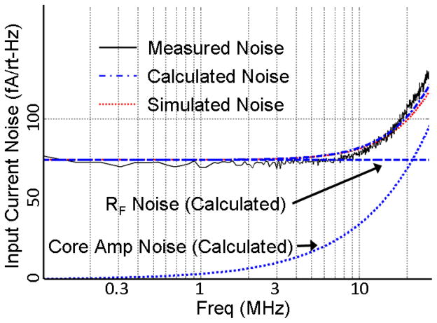
Fig. 13 plots the measured, simulated and the theoretically expected input referred noise of the monolithically integrated TIA for a 3 MΩ feedback resistance. The measured input referred noise is obtained by dividing the measured output noise of the TIA by the TIA transfer function. The theoretical noise contribution of the feedback resistor and the core amplifier are shown separately along with the total calculated TIA noise. A 100 fF capacitance mimics the CMUT at the input of the amplifier in simulations. The theoretical core amplifier noise is calculated using the 1.1 nV/√Hz amplifier voltage noise and the 500 fF total input capacitance, which includes the CMUT capacitance and the amplifier input capacitances. The noise increase at higher frequencies is also visible from the plot. It can be seen that the measured noise matches well with the total calculated and simulated noise values.
Fig. 13.
The measured and simulated input current noise of the TIA. The total theoretically calculated noise is also plotted along with the calculated feedback resistance noise and the calculated core amplifier noise. The measured 75 fA/√Hz feedback noise level at low frequencies is equivalent to the current noise of a 3 MΩ resistor.
The monolithically integrated 3 MΩ feedback TIA achieves an input referred noise current density performance of 90 fA/√Hz around 15 MHz. Total integrated TIA noise is 0.29 nA over 10 to 20 MHz CMUT band. This value was also verified from a time domain measurement of the TIA noise using an oscilloscope. The maximum input current that the amplifier can handle can be determined by the level where the amplifier gain changes by 1 dB from its small signal value. From simulations, the maximum peak to peak input current is found to be 20 nA. The 1 dB gain change point is also measured using the test setup shown in Fig. 10. In the measurement, the maximum input current is found to be 37 nA. The difference between the simulated and the measured values is due to the typical process variation in the transistors when compared to the nominal model values in simulation. Considering the 0.29 nA input noise floor and the maximum nominal (simulated) peak to peak input current of 20 nA the preamplifier has 28 dB dynamic range. The dynamic range should be improved to at least 40 dB for satisfactory IVUS image performance. The major source of nonlinearity in the amplifier is the overdrive voltage of the feedback transistor that limits the maximum voltage swing at the TIA output. To implement the 3 MΩ resistance with the triode region NMOS with the aspect ratio of 0.4μm/4μm, the required Vctrl – VOUT – VT term in (9) is simulated to be around 44 mV. This overdrive voltage can be easily improved, while keeping the effective resistance the same, by using a longer feedback transistor. For instance, increasing the length of the transistor 4 times should also increase the maximum input current by 4 times and hence improve the dynamic range by 12 dB. Alternatively, to improve the dynamic range, the high feedback resistance can be implemented with a T-network of resistors [28].
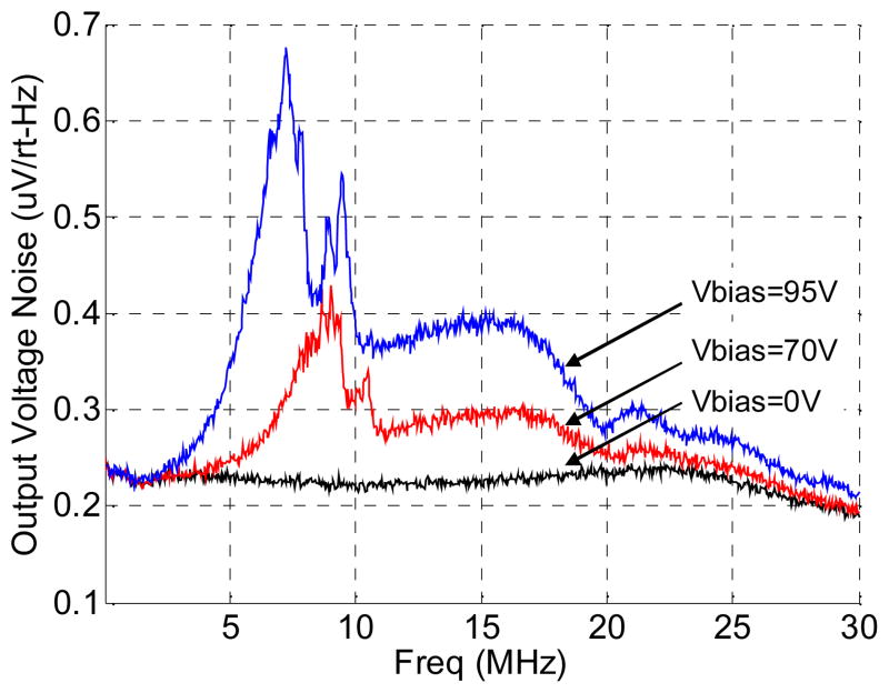
Ideally receiver electronics noise contributions should be less than the CMUT thermal-mechanical noise. To obtain measurements of the total system noise in immersion including the CMUT thermal-mechanical noise, a monolithically integrated IC was placed in a water tank. The output noise spectrum of the system at different CMUT bias voltages was measured (Fig. 14). The output at 0V represents the noise of the receiver electronics. As the CMUT bias is increased, the coupling coefficient and hence the CMUT noise contribution increases. Furthermore, as the CMUT bias is increased, the equivalent CMUT resistance decreases. For 0V bias the effective resistance is infinite and for the highest CMUT bias RCMUT is calculated to be close to 1MΩ. In Fig. 8, it was shown that the amplifier noise is independent of the CMUT resistance when the CMUT resistance is higher than 20 kΩ. Therefore the changing CMUT resistance does not modify the amplifier noise. On the other hand, with increasing bias, as the vacuum gap decreases, the CMUT capacitance increases to 150 fF from its 0V bias value of 100 fF. This increases the CCMUT term in (4) and results in a slight increase in the part of the amplifier noise that increases with frequency. However, the change in the CMUT capacitance is much smaller when compared to the total capacitance value at the input, which is around 500 fF. Therefore the increase in the amplifier noise with the increasing CMUT bias is expected to be very small. The frequency span of the CMUT noise is larger than the operation band of the device in immersion, which is from 10 MHz to 20 MHz. The source of the CMUT noise contribution from 5 MHz to 10 MHz is suspected to be due to the acoustic crosstalk and the spurious waves in the substrate.
Fig. 14.
The system noise with 0V, 70V and 95V CMUT biases. When there is no dc bias, the noise is only due to the front-end electronics. As the DC bias is increased, the CMUT noise starts to dominate the system noise clearly demonstrating the transducer noise-limited receiver performance.
Fig. 14 clearly indicates that the CMUT thermal-mechanical noise dominates the output noise for 95V DC bias, close to collapse voltage. The preamplifier noise figure can be calculated by using the ratio of the total noise power to the noise power of the CMUT. Comparing the noise powers at 0V bias and 95V bias in the CMUT frequency band (10–20 MHz), it is seen that the CMUT noise accounts for 66% of the total noise power. Therefore, the noise figure (NF) is calculated as 1.8 dB.
An important figure of merit for CMUT system performance is the input referred pressure noise. If one predicts the noise of an ideal CMUT, the minimum noise pressure due to the radiation impedance is where Rmed is the real part of the radiation impedance in Rayls and S is the area of the transducer [32]. For the particular FL array element, this ideal CMUT noise can be calculated to be 2.3 mPa/√Hz where the radiation impedance of the CMUT element is considered equivalent to that of a circular piston with a 40 μm radius.
The noise equivalent pressure is experimentally found by using the measured output voltage noise in Fig. 14 and a receive sensitivity measurement. The receive sensitivity measurement based on the hydrophone measurements showed a 130 mV/kPa sensitivity at the TIA output when the CMUT is biased close to collapse. The noise equivalent pressure of the total system including the CMUT noise and the receiver circuitry noise is then found to be 3 mPa/√Hz at the center frequency. Based on this measured total noise equivalent pressure, Fig. 14 suggests an amplifier noise of 1.8 mPa/√Hz and a CMUT noise of 2.4 mPa/√Hz. This measured CMUT noise is very close to the ideal case CMUT noise prediction of 2.3 mPa/√Hz, which considered the noise due to the radiation impedance and ignored the CMUT electrical and mechanical losses.
Table II compares the performance of front end receivers in literature that were designed for CMUT devices with the noted bandwidth and sizes. It can be seen that the TIA design in this work achieves the smallest noise figure. In [26], although its front-end is electronics noise limited, a smaller noise equivalent pressure is reported mainly due to a larger sized CMUT element. In addition, studies in [10, 26] use the same element as the receiver and transmitter and therefore requires protection circuitry to protect the low voltage receiver amplifiers from high voltage pulses. This protection circuitry introduces additional noise and degrades the receiver noise performance. One of the advantages of having separate rings for receive and transmit operation is that there is no necessity for a TX-RX switch and a receiver protection circuitry, which is advantageous for low-noise detection.
TABLE II.
The Performance Comparison of Receiver Front-End Designs for CMUT Integration
VII. Conclusion
The monolithic CMUT-CMOS integration offers improved overall sensor performance, smaller size and easier packaging with a small number of external connections. We discussed the design and implementation of a custom ASIC that is designed and fabricated in a 0.35 μm CMOS process for monolithic integration with a forward-looking CMUT array consisting of 70 μm × 70 μm elements. In the receiver design, the trade-offs between the gain, bandwidth, noise performance and the power consumption are discussed in detail. The transistor-feedback TIA design is shown to reduce the parasitic feedback capacitances and improve the low noise design at the expense of reduced linearity. Methods are available to improve the linearity for future designs. The successful monolithic integration of the CMUT array with the ASIC is demonstrated through a pulse-echo measurement. It is shown that the monolithic integration and the custom electronics designed for minimum noise enable transducer noise-dominated receiver performance with an input referred current noise density performance of 90 fA/√Hz and a 1.8 dB noise figure.
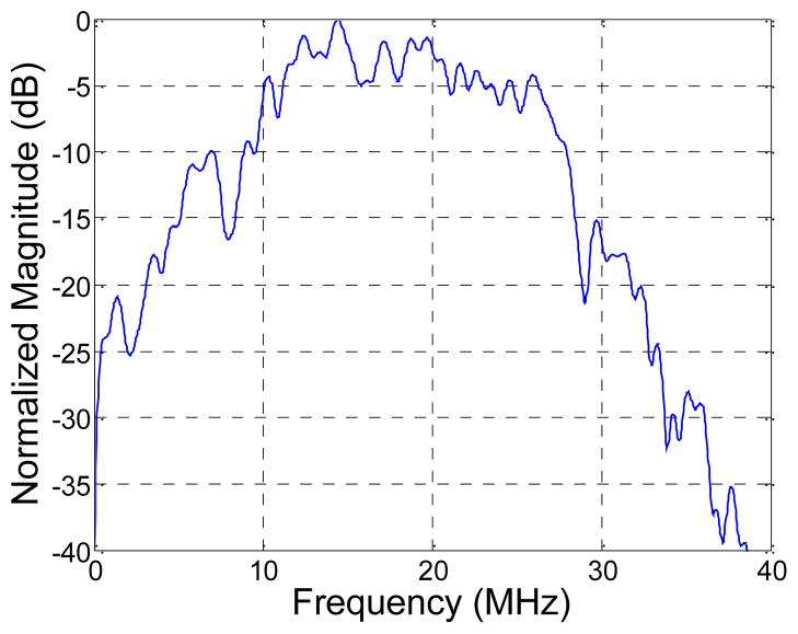
Fig. 6.
The normalized frequency response of the pulse-echo shown in Fig. 5. The center frequency is 15.2 MHz.
TABLE I.
Summary of the Key TIA and CMUT Parameters
| TIA PARAMETERS | |
| Technology | 0.35 μm CMOS |
| Power Supply | 3.3 V |
| TIA Area | 70 μm * 140 μm |
| TIA Power Consumption | 6.6 mW |
| TIA Gain | 3 MΩ |
| TIA Bandwidth | 20 MHz |
| TIA Input Current Noise Density | 90 fA/√Hz |
| Buffer Power Consumption | 3.3 mW |
| CMUT PARAMETERS | |
| Operation Freq | 10 – 20 MHz |
| Element Area | 70 μm × 70 μm |
| RCMUT (calculated) | 1 MΩ |
| CCMUT (calculated) | 150 fF |
Acknowledgments
The authors want to thank Jaime Zahorian, Michael Hochman, Toby Xu, and Sarp Satir for the fabrication of CMUTs and their support for the experiments. This work was supported by Award Number R01EB010070 from the National Institute of Biomedical Imaging and Bioengineering, and Award Number R01HL082811 from the National Heart, Lung and Blood Institute.
References
- 1.van der Steen AF, Baldewsing RA, Degertekin FL, Emelianov S, Frijlink ME, Furukawa Y, Goertz D, Karaman M, Khuri-Yakub PT, Kim K. IVUS beyond the horizon. EuroIntervention. 2006;2:132. [PubMed] [Google Scholar]
- 2.Garcia-Garcia HM, Costa MA, Serruys PW. Imaging of coronary atherosclerosis: intravascular ultrasound. European Heart Journal. 2010;31:2456–2469C. doi: 10.1093/eurheartj/ehq280. [DOI] [PubMed] [Google Scholar]
- 3.Oralkan O, Ergun AS, Johnson JA, Karaman M, Demirci U, Kaviani K, Lee TH, Khuri-Yakub BT. Capacitive micromachined ultrasonic transducers: next-generation arrays for acoustic imaging? Ultrasonics, Ferroelectrics and Frequency Control, IEEE Transactions on. 2002;49:1596–1610. doi: 10.1109/tuffc.2002.1049742. [DOI] [PubMed] [Google Scholar]
- 4.Yeh DT, Oralkan O, Wygant IO, Donnell MO, Khuri-Yakub BT. 3-D ultrasound imaging using a forward-looking CMUT ring array for intravascular/intracardiac applications. IEEE Transactions on Ultrasonics Ferroelectrics and Frequency Control. 2006;53:1202. doi: 10.1109/tuffc.2006.1642519. [DOI] [PubMed] [Google Scholar]
- 5.Degertekin FL, Guldiken RO, Karaman M. Annular-ring CMUT arrays for forward-looking IVUS: transducer characterization and imaging. Ultrasonics, Ferroelectrics and Frequency Control, IEEE Transactions on. 2006;53:474–482. doi: 10.1109/tuffc.2006.1593387. [DOI] [PubMed] [Google Scholar]
- 6.Daft C, Panda S, Wagner P, Ladabaum I. Two approaches to electronically scanned 3D imaging using cMUTs. Ultrasonics Symposium; 2006; IEEE. 2006. pp. 685–688. [Google Scholar]
- 7.Wygant IO, Zhuang X, Yeh DT, Oralkan O, Ergun AS, Karaman M, Khuri-Yakub BT. Integration of 2D CMUT arrays with front-end electronics for volumetric ultrasound imaging. IEEE Transactions on Ultrasonics Ferroelectrics and Frequency Control. 2008;55:327–342. doi: 10.1109/TUFFC.2008.652. [DOI] [PubMed] [Google Scholar]
- 8.Wang Y, Stephens DN, O’Donnell M. Optimizing the beam pattern of a forward-viewing ring-annular ultrasound array for intravascular imaging. Ultrasonics, Ferroelectrics and Frequency Control, IEEE Transactions on. 2002;49:1652–1664. doi: 10.1109/tuffc.2002.1159845. [DOI] [PubMed] [Google Scholar]
- 9.Demirci U, Ergun AS, Oralkan O, Karaman M, Khuri-Yakub BT. Forward-viewing CMUT arrays for medical imaging. Ultrasonics, Ferroelectrics and Frequency Control, IEEE Transactions on. 2004;51:887–895. doi: 10.1109/tuffc.2004.1320749. [DOI] [PubMed] [Google Scholar]
- 10.Nikoozadeh A, Oralkan O, Gencel M, Jung Woo C, Stephens DN, de la Rama A, Chen P, Thomenius K, Dentinger A, Wildes D, Shivkumar K, Mahajan A, O’Donnell M, Sahn D, Khuri-Yakub PT. Forward-looking volumetric intracardiac imaging using a fully integrated CMUT ring array. Ultrasonics Symposium (IUS); 2009; IEEE International. 2009. pp. 511–514. [Google Scholar]
- 11.Eccardt PC, Niederer K, Scheiter T, Hierold C. Surface micromachined ultrasound transducers in CMOS technology. Ultrasonics Symposium, 1996. Proceedings; 1996; IEEE. 1996. pp. 959–962. [Google Scholar]
- 12.Tang PK, Wang PH, Li ML, Lu MSC. Design and characterization of the immersion-type capacitive ultrasonic sensors fabricated in a CMOS process. Journal of Micromechanics and Microengineering. 2011;21:025013. [Google Scholar]
- 13.Doody CB, Cheng X, Rich CA, Lemmerhirt DF, White RD. Modeling and Characterization of CMOS-Fabricated Capacitive Micromachined Ultrasound Transducers. Microelectromechanical Systems, Journal of. 2011;20:104–118. [Google Scholar]
- 14.Daft C, Wagner P, Bymaster B, Panda S, Patel K, Ladabaum I. cMUTs and electronics for 2D and 3D imaging: monolithic integration, in-handle chip sets and system implications. Ultrasonics Symposium; 2005; IEEE. 2005. pp. 463–474. [Google Scholar]
- 15.Noble RA, Davies RR, Day MM, Koker L, King DO, Brunson KM, Jones ARD, McIntosh JS, Hutchins DA, Robertson TJ, Saul P. Cost-effective and manufacturable route to the fabrication of high-density 2D micromachined ultrasonic transducer arrays and (CMOS) signal conditioning electronics on the same silicon substrate. Ultrasonics Symposium; 2001; IEEE. 2001. pp. 941–944. [Google Scholar]
- 16.Zahorian J, Guldiken R, Gurun G, Qureshi MS, Balantekin M, Hasler P, Degertekin FL. Single chip CMUT arrays with integrated CMOS electronics: Fabrication process development and experimental results. Ultrasonics Symposium, 2008. IUS; 2008; IEEE. 2008. pp. 386–389. [Google Scholar]
- 17.Graeme J. Photodiode Amplifiers: Op Amp Solutions. New York: McGraw-Hill; 1995. [Google Scholar]
- 18.Singh T, Saether T, Ytterdal T. Feedback biasing in nanoscale CMOS technologies. Circuits and Systems II: Express Briefs, IEEE Transactions on. 2009;56:349–353. [Google Scholar]
- 19.Cicek I, Bozkurt A, Karaman M. Design of a front-end integrated circuit for 3D acoustic imaging using 2D CMUT arrays. Ultrasonics, Ferroelectrics and Frequency Control, IEEE Transactions on. 2005;52:2235–2241. doi: 10.1109/tuffc.2005.1563266. [DOI] [PubMed] [Google Scholar]
- 20.Sheng-Yu P, Qureshi MS, Hasler PE, Basu A, Degertekin FL. A Charge-Based Low-Power High-SNR Capacitive Sensing Interface Circuit. Circuits and Systems I: Regular Papers, IEEE Transactions on. 2008;55:1863–1872. doi: 10.1109/TCSI.2008.918006. [DOI] [PMC free article] [PubMed] [Google Scholar]
- 21.Ciofi C, Crupi F, Pace C, Scandurra G. Improved trade-off between noise and bandwidth in op-amp based transimpedance amplifier. Instrumentation and Measurement Technology Conference, 2004. IMTC 04. Proceedings of the 21st IEEE; 2004. pp. 1990–1993. [Google Scholar]
- 22.Ferrari G, Gozzini F, Molari A, Sampietro M. Transimpedance Amplifier for High Sensitivity Current Measurements on Nanodevices. Solid-State Circuits, IEEE Journal of. 2009;44:1609–1616. [Google Scholar]
- 23.Oralkan O. PhD dissertation, Dept Elect Eng. Stanford Univ; 2004. Acoustical Imaging Using Capacitive Micromachined Ultrasonic transducer Arrays Devices Circuits and Systems. [Google Scholar]
- 24.Gurun G, Qureshi MS, Balantekin M, Guldiken R, Zahorian J, Sheng-Yu P, Basu A, Karaman M, Hasler P, Degertekin L. Front-end CMOS electronics for monolithic integration with CMUT arrays: Circuit design and initial experimental results. Ultrasonics Symposium, 2008. IUS; 2008; IEEE. 2008. pp. 390–393. [Google Scholar]
- 25.Black WC, Jr, Stephens DN. CMOS chip for invasive ultrasound imaging. Solid-State Circuits, IEEE Journal of. 1994;29:1381–1387. [Google Scholar]
- 26.Wygant I, Jamal N, Lee H, Nikoozadeh A, Oralkan O, Karaman M, Khuri-yakub B. An integrated circuit with transmit beamforming flip-chip bonded to a 2-D CMUT array for 3-D ultrasound imaging. Ultrasonics, Ferroelectrics and Frequency Control, IEEE Transactions on. 2009;56:2145–2156. doi: 10.1109/TUFFC.2009.1297. [DOI] [PubMed] [Google Scholar]
- 27.Gurun G, Zahorian J, Hasler P, Degertekin FL. Thermal Mechanical Noise Based Characterization of CMUTs Using Monolithically Integrated Low Noise Receiver Electronics. Ultrasonics Symposium, 2010. IUS; 2010; IEEE. 2010. p. to be printed. [Google Scholar]
- 28.Sharma A, Zaman MF, Ayazi F. A 104-dB Dynamic Range Transimpedance-Based CMOS ASIC for Tuning Fork Microgyroscopes. Solid-State Circuits, IEEE Journal of. 2007;42:1790–1802. [Google Scholar]
- 29.Behzad R. Design of Integrated Circuits for Optical Communications. McGraw-Hill, Inc; 2003. [Google Scholar]
- 30.T. Instruments. OPA657 - 1.6GHz, Low-Noise, FET-Input Operational Amplifier. 2008. [Google Scholar]
- 31.Vanisri T, Toumazou C. Integrated high frequency low-noise current-mode optical transimpedance preamplifiers: theory and practice. Solid-State Circuits, IEEE Journal of. 1995;30:677–685. [Google Scholar]
- 32.Wygant IO, Zhuang X, Yeh DT, Vaithilingam S, Nikoozadeh A, Oralkan O, Ergun AS, Karaman M, Khuri-Yakub BT. An endoscopic imaging system based on a two-dimensional CMUT array: real-time imaging results. Ultrasonics Symposium; 2005; IEEE. 2005. pp. 792–795. [Google Scholar]


