Abstract
We present a novel surface plasmon resonance (SPR) configuration based on narrow groove (sub-15 nm) plasmonic nano-gratings such that normally incident radiation can be coupled into surface plasmons without the use of prism-coupling based total internal reflection, as in the classical Kretschmann configuration. This eliminates the angular dependence requirements of SPR-based sensing and allows development of robust miniaturized SPR sensors. Simulations based on Rigorous Coupled Wave Analysis (RCWA) were carried out to numerically calculate the reflectance - from different gold and silver nano-grating structures - as a function of the localized refractive index of the media around the SPR nano-gratings as well as the incident radiation wavelength and angle of incidence. Our calculations indicate substantially higher differential reflectance signals, on localized change of refractive index in the narrow groove plasmonic gratings, as compared to those obtained from conventional SPR-based sensing systems. Furthermore, these calculations allow determination of the optimal nano-grating geometric parameters - i. e. nanoline periodicity, spacing between the nanolines, as well as the height of the nanolines in the nano-grating - for highest sensitivity to localized change of refractive index, as would occur due to binding of a biomolecule target to a functionalized nano-grating surface.
OCIS codes: (240.6680) Surface plasmons, (050.1755) Computational electromagnetic methods, (260.2110) Electromagnetic optics, (260.3910) Metal optics, (160.4236) Nanomaterials, (280.4788) Optical sensing and sensors
1. Introduction
Plasmon resonances in metallic nanostructures - thin films, nanopillars fabricated on planar surfaces, and nanoparticles - are collective oscillations of the conduction band electrons, which are excited when radiation of certain wavelengths is incident on these nanostructures. Excitation of surface plasmons leads to an increase in the electromagnetic fields in the vicinity of metallic thin films and nanostructures and this has been exploited for the fabrication of surface plasmon resonance (SPR) based [1–7], localized surface plasmon resonance (LSPR) based [8–12] and surface-enhanced Raman scattering (SERS) based [13–17] sensors. Plasmon resonances of noble metal nanostructures (mainly gold and silver) are conventionally employed for developing SPR, LSPR, and SERS based sensors as these nanostructures resonantly scatter or absorb light in the visible and near-infrared spectra. SPR sensors are conventionally based on detecting changes of refractive indices - both in the bulk media around the metallic films or in the vicinity of the continuous metallic films having nano-scale thickness, conventionally between 30 and 60 nm - employing both angular and wavelength interrogation methods. SPR imaging (SPRI) sensors [18–20] have also been employed for chemical and biological sensing applications. SPRI sensors are based on detection of differential reflectance - before and after the localized changes of refractive indices on the surface of the plasmonic films - for the entire imaging region, given constant radiation wavelength and angle of incidence such that these satisfy the conditions for surface plasmon resonance excitation in the metallic films. Mostly, SPR sensors employ either prism coupling as shown in Fig. 1a (Kretschmann or Otto configurations) or grating-based [1-2], or waveguide coupling (which includes optical fiber waveguides [1-2]) for coupling of the incident radiation into surface plasmons. SPR is employed for sensitive and label-free biosensing of analyte molecules that adsorb or bind on the surface of the metallic thin film (of a plasmonics-active material such as gold, silver, or copper) thereby changing the oscillation of the surface plasmons, which in turn effects the modulation of the light reflected form the metallic thin film [1–7]. This modulation could be monitored by the angular distributions of reflection and transmission, wavelength, intensity, phase, and polarization changes. On the other hand, the LSPR based sensors are conventionally based on detecting changes in the localized refractive indices - in the vicinity (less than 10 nm away from the surface of the nanostructures) of metallic nanoparticles or nanopillars fabricated on planar surfaces - by detecting the shifts in the plasmon resonance wavelengths associated with the nanostructures (includes individual nanostructures as well as clusters and arrays of these nanostructures). The localized refractive index changes may be caused due to deposition or binding of certain molecules or other materials on the surface of the nanostructures. There are limits on the sensitivities of the conventional SPR sensors [21–22] and some recent research has involved studying the effect of nano-structuration of the metallic thin films for increasing the sensitivity of these sensors [23–25]. Theoretical calculations by Byun et al. [23] indicate that an increase in sensitivity is to be expected for nanostructured gold films. While Masson et al. [24] have shown increased sensitivity to localized refractive index changes by developing arrays of nanoholes in gold films, Malic et al. [25] have demonstrated an increase in sensitivity of biomolecular detection by employing nanopillar arrays. On the other hand, nanohole arrays [26-33] in metallic thin films have also been extensively employed for sensing applications. Most of these studies have lead to a modest increase in the sensitivity of the sensors over that of metallic thin films employed for SPR or SPRI based sensing.
Fig. 1.
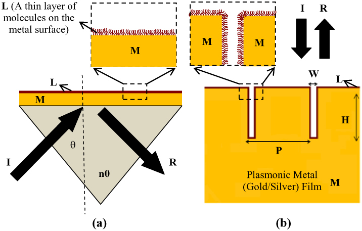
(a) Schematic showing Kretschmann configuration conventionally employed for coupling of the incident radiation to surface plasmons and (b) Schematic showing narrow groove plasmonic (gold or silver) nano-grating structure illustrating the important dimensions and parameters. The incident and reflected radiation are indicated by symbols ‘I’ and ‘R’, respectively. While ‘M’ indicates a plasmonic film such as a gold or silver film, ‘L’ indicates a thin layer of molecules on the surface of the metallic film. ‘(P)’ and ‘(H)’ shown in the above figure indicate the periodicity and height of the nanolines in the nano-gratings and ‘(W)’ indicates the spacing between adjacent nanolines in the nano-grating.
In this paper, we describe a novel SPR sensor platform - that does not employ the Kretschmann configuration and is based on direct coupling of normally incident radiation into narrow groove metallic nano-gratings - that is very sensitive to localized changes in refractive index in the vicinity of the metallic surface of the nano-gratings. The sensing approach described in this paper does not require any prism coupling mechanism thereby enabling capability of miniaturization of these sensors. Moreover, the sensing mechanism is based on normal incidence of radiation on the sensor surface thereby removing any stringent coupling angle requirements as in the conventional Kretschmann based SPR sensors. The calculations described in this paper elucidate that very high values of differential reflectance signals (between reflectance signals before and after localized changes of refractive indices on the surface of the metallic nano-gratings) are obtained when the optimal configuration (periodicity, filling factor, height) of the nano-grating structures are employed. The simple one-dimensional nano-grating structures described in this paper can be fabricated without much difficulty. Moreover, we illustrate that the nano-grating sensors are not very sensitive to bulk changes in refractive index thereby making them very robust and less sensitive to temperature variations (and therefore temperature-dependent refractive index variations) in the bulk refractive index around the nano-gratings.
Narrow groove metallic gratings exhibit direct coupling of normally incident radiation to surface plasmons. Wirgin et al. [34] derived mathematical relationships between the electric and magnetic fields in between rectangular grooves in zero-order silver gratings and demonstrated a substantial increase in the electric field intensity inside the grooves as the spacing between the metallic gratings decreased. Tan et al. [35] and Garcia Vidal et al. [36] explained the phenomenon of coupling of p-polarized incident radiation to surface plasmon polariton (SPP) modes in short-pitch metallic gratings [37–41]. The narrow width of the grooves leads to strong coupling between surface charges on opposing walls of an individual grating groove, thereby leading to formation of standing SPP modes localized inside the groove. The coupling between the SPP modes inside the individual grooves increases with decreasing groove width. Each SPP standing mode in the individual grooves couples to the corresponding mode in the neighboring grooves leading to formation of very flat SPP bands. Due to the generation of a series of standing SPP modes inside each groove, the dispersion relation (ω-kx relationship) of the grating has multiple points of intersection with the light line (dispersion relation of the incident radiation, kx = ω/c) indicating coupling of multiple wavelengths to the SPP modes in the individual grooves in the grating. The narrow groove plasmonic nano-gratings described in this paper are different from the one-dimensional plasmonic gratings [42] or two-dimensional nanohole arrays [26-29] employed conventionally for coupling of the incident radiation into surface plasmons as in those gratings the coupling of the incident radiation occurs when the wave vector of surface plasmons is the sum of the wave vectors of the incident radiation in the direction of the surface plasmon wave propagation and the allowed momentum vectors of the periodic structure of the one-dimensional gratings or the nanohole arrays.
Garcıa-Vidal et al. [36] have described theoretical calculations for EM fields around a metallic reflection grating schematically shown in Fig. 1b - a metallic film having periodic rectangular grooves with a periodicity ‘P’ and λ>P and the length of the grooved surface being infinitely long in one direction - on which p-polarized light (having wavelength λ) is incident normally. Garcıa-Vidal et al. [36] showed that the enhancement of the electric-field intensity inside the grooves as a function of the incident field (the electric field inside the grooves i.e. Egroove in terms of the incident electric field i.e. Eincident) is proportional to (P/W)2 in the case of cavity resonances (λ>>H), when sin(k0 H) = 1. This explains the increase of EM field enhancement as the nano-scale gap ‘W’ between the metallic nano-gratings is decreased.
We describe theoretical studies of employing the metallic (both gold and silver) nano-gratings for surface plasmon sensing of localized changes of refractive index on the surface of the nano-gratings such as those caused by binding events such as DNA-DNA binding or antigen-antibody binding or deposition of very thin layers (such as monolayers) of molecules or other materials. We study the sensitivity of the surface plasmon sensing, more specifically the effect on differential reflectance before and after the change of the localized refractive index in the vicinity of the nano-grating surface. In order to demonstrate the high sensitivity of the plasmonic nano-gratings over continuous plasmonic thin films, we provide comparisons between differential reflectance signals obtained from the change of the localized refractive index in the vicinity of a continuous thin metallic film - in which the surface plasmons are coupled using the Kretschmann configuration - with the nano-gratings on which the radiation is incident normally and no Kretschmann coupling mechanism is required. We compare the reflection spectra calculations for nano-gratings of non-plasmonic materials such as titanium, silicon, and silicon-dioxide with those from plasmonic materials such as silver and gold and show that the plasmon resonance peaks are visible only for nano-gratings of the plasmonic metals (silver and gold). We describe the effect of periodicity, filling factor, and height on the plasmon resonance wavelengths as well as the plasmonic wavelength band structure associated with the plasmonic nano-gratings. Moreover, we study the effect of these parameters on the sensitivity of the surface plasmon sensing, more specifically the effect on differential reflectance before and after the change of the localized refractive index in the vicinity of the nano-grating surface. The effect of decreasing the nano-scale gaps between the lines of the nano-gratings, on the sensitivity of the surface plasmon sensing, was also studied. It has to be noted that the plasmonic nano-gratings described in this paper having sub-15 nm gaps are possible to fabricate due to the recent advances in nanofabrication capabilities [43–55]. While electron beam lithography [43,44] and focused ion beam milling [45–48] of metallic nanostructures can allow development of plasmonic nano-grating structures with sub-20 nm spacing between the nanolines, recent research has led to the development of some novel fabrication techniques [49–54] that can potentially allow the development of sub-10 nm spacings between the metallic nanostructures. The current state-of-the-art as well as the recent developments in nanolithography can enable the development of the narrow groove nano-grating structures that are described in this paper; thereby making the concept of employing of narrow groove plasmonic nano-grating structures for surface plasmon resonance sensing more viable and practical.
2. Numerical simulations based on rigorous coupled wave analysis (RCWA) and finite-difference time-domain (FDTD) simulations
2-D Rigorous Coupled Wave Analysis (RCWA) calculations [56–58] of reflectance from the metallic nano-grating structures was carried out using an software called DiffractMOD 3.1. The DiffractMOD software calculates the diffraction efficiency and field distribution for 2D or 3D periodic structures such as the nano-grating structures described in this work and is extensively employed for the design and modelling of photonic structures and devices such as subwavelength structures, photonic bandgap crystals, and other grating-assisted devices. The DiffractMOD 3.1 software is based on Rigorous Coupled Wave Analysis (RCWA) and Modal Transmission Line theory (MTL). RCWA algorithms allow a full vectorial solution of the Maxwell's equations in the Fourier domain, wherein periodic permittivity functions are represented using Fourier harmonics and the electromagnetic fields are represented as summations over coupled waves.
In the RCWA calculations carried out for the gold and silver nano-grating structures, TM polarized plane waves (at different wavelengths of incidence) were incident normally at the grating structures (Fig. 1b) and the reflectance calculated as a function of the incident wavelength. Firstly, the effect of nanoline dimensions - such as periodicity ‘P’, spacing ‘W’, and height ‘H’ (Fig. 1b) - on the plasmon resonance wavelength associated with the nanowire structures was calculated. Tuning of the nano-grating dimensions - to tune the plasmon resonances associated with the metallic nanoline structures - is important to ensure that the plasmon resonance sensing based on the nanoline gratings could be carried out in different spectral regimes. Moreover, it allows tuning of the plasmon resonance wavelengths to those of conventional light sources (both LEDs and Lasers). The RCWA calculations were carried out to determine the effect of varying the refractive index of bulk media around the nano-gratings as well as localized changes of refractive index (such as those caused by binding of a biomolecule target to a functionalized nano-grating surface). This software enables RCWA analysis of the metallic media to include dispersion relations of the dielectric constants of the metals [59]. RCWA analysis significantly decreases computational time and required memory size as compared to the FDTD method and was therefore employed to calculate the wavelength and angular dependence of the reflectance from metal-coated nanowire gratings.
Finite-Difference Time-Domain algorithms [60] analyze structures by solving the differential form of coupled Maxwell’s equations. Our group has previously employed FDTD for modeling electromagnetic fields around metallic nanostructures of different geometries [46, 59]. In this work, we employed an FDTD software called FullWAVE 6.0 by R-Soft to carry out analysis for our plasmonic nanostructures. FDTD analysis described in these calculations incorporates the effects of dispersion relations, i. e. the effects of wavelength dependence of the dielectric constants of the metallic structures, such as the Debye or Lorentz models. In the simulations, we use an extended Debye dispersion model for determining the dielectric constant for gold and silver [59]. 2-D solutions were obtained for electromagnetic fields around the gold and silver nanoline gratings. Electromagnetic fields (i. e. E and H fields in the x, y, and z directions) in the vicinity of the metallic nanoline gratings were calculated assuming plane wave illumination, with wavelengths varying between 300 nm and 1200 nm. The magnitude of the incident electric fields was taken to be unity and the enhancement of electromagnetic fields, around the nano-gratings, evaluated. The time steps (Δt) employed in these simulations were selected to be small enough such that the Courant stability criterion [60] was satisfied. For FDTD calculations involving the plasmonic nano-gratings, the grid sizes in x, y, and z directions (Δx, Δy, and Δz) were selected to be such that the value of the E field intensities around the nano-gratings became independent of the grid sizes.
3. Results and discussions
The narrow groove nano-grating based SPR sensors are substantially different from conventional SPR sensors that employ the Kretschmann or Otto configurations. They do not require any prism coupling mechanism and are based on normal incidence of radiation on the sensor surface. This removes the stringent coupling angle requirements as in the conventional Kretschmann based SPR sensors and can also enable miniaturization of these sensors. Along with these advantages, we also observe from Fig. 2 that the narrow groove nano-grating sensors are more sensitive to localized changes in refractive index as compared with the conventional Kretschmann based SPR sensors. Figure 2 shows rigorous coupled wave analysis (RCWA) calculations showing shifts in the plasmon resonance dips in the reflectance spectra as a 1 nm thick film, having a refractive index of 1.53, is deposited on the surface of the gold and silver films and narrow groove nano-gratings shown in Fig. 1. While Figs. 2a and 2b show RCWA calculations for the reflectance spectra for gold and silver continuous thin films (30 −60 nm thick) acquired using the angular interrogation method, Figs. 2c and 2d show RCWA calculations for the reflectance spectra for gold and silver continuous thin films acquired using the spectral interrogation method. One can observe from Figs. 2a and 2b that the maximum value of the differential reflectance signal is 0.094 or 9.4% and 0.038 or 3.8% for silver and gold continuous films respectively when the calculations are carried out using the angular interrogation method at 660 nm wavelength. Employing the spectral interrogation method, the maximum values of the differential reflectance signals are 0.1077 or 10.77% and 0.082 or 8.2% for silver and gold continuous films - the maxima in the differential reflectance signals occurring at 1035 nm and 1037 nm for silver and gold, respectively. The angles of incidence - at which the maxima in the differential reflectance signals were observed for silver and gold continuous thin films - were 63.5 and 63.8 degrees respectively. Moreover, the minima in the minimum value being −0.0396) for silver and gold continuous films, respectively. Employing the spectral interrogation method, the maximum values of the differential reflectance signals are 0.101 or 10.1% and 0.0529 or 5.29% for silver and gold continuous films respectively when the plasmon resonance related dips in the reflectance spectra (before and after the localized refractive index change) - as well as the maxima and the minima in the differential reflectance curves - lie in the spectral regions less than 800 nm (see Figs. 2c and 2d). The angles of incidence - at which the maxima in the differential reflectance signals were observed for silver and gold continuous thin films when the wavelength of the incident radiation is below 800 nm - were 66 and 68 degrees respectively.
Fig. 2.
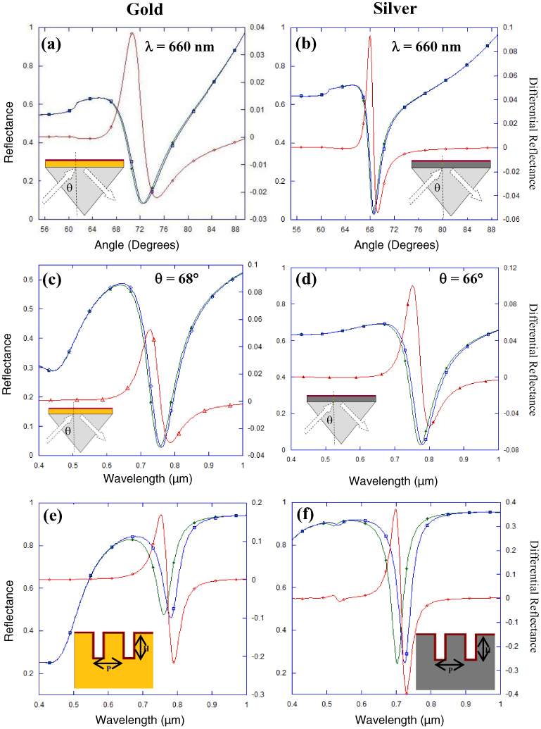
Rigorous coupled wave analysis (RCWA) calculations showing reflectance curves with localized refractive index around the film being 1.33 in green and 1.53 (n=1.53 for 1 nm above the metallic film, the remaining region having n=1.33) in blue for a planar metallic film (50 nm plasmonics-active metal and 5 nm Ti) deposited on a BK7 glass prism employed for SPR measurements. Reflectance and differential reflectance plots for angular interrogation are provided, the plasmonic metal being (a) Gold and (b) Silver. Reflectance and differential reflectance plots are provided for spectral interrogation, the plasmonic metal being (c) Gold and (d) Silver. RCWA calculations showing reflectance curve (differential reflectance in red, reflectance curves with localized refractive index around the grating n=1.33 in green and with n = 1.53 in blue) for a narrow groove metallic nano-grating (with 100 nm height and periodicity as well as 7 nm groove width) for a 1nm binding of target (refractive index = 1.53) on the surface of the metallic film for (e) Gold nano-grating, and (f) Silver nano-grating.
On the other hand, when narrow groove nano-gratings - with 100 nm height ‘H’ and periodicity ‘P’ and 7 nm groove width ‘W’ - are employed for SPR sensing of a 1 nm thin film on the metallic film surface, the differential signal is 0.373 or 37.3% for silver nano-gratings and 0.017 or 17% for gold nano-gratings. Even when the planar gold films are normalized for the surface area - such that they have equivalent surface area as the nano-gratings with 100 nm height ‘H’ and periodicity ‘P’ and a 7 nm groove width ‘W’, the area of these nano-gratings being ~3 times that of a continuous metallic films - the values of the normalized differential reflectance signals for silver and gold films are 0.26 or 26% and 0.093 or 9.3% respectively, which are lower than the values for the differential reflectance signals from silver and gold nano-gratings (37% and 17% respectively). When the values of ‘H’, ‘P’ and ‘W’ are optimized to obtain the maximum value of the differential signals, one could observe values as high as 0.75 or 75% for silver and 0.63 or 63% for gold films (when the values of ‘H’ and periodicity ‘P’ are 50 nm and 100 nm respectively and groove width ‘W’ is 3 nm) and 0.66 or 66% for silver and 0.52 or 52% for gold films (when the values of ‘H’ and periodicity ‘P’ are 50 nm and 100 nm respectively and groove width ‘W’ is 4 nm). These calculations highlight that very high values of differential reflectance signals (between reflectance signals before and after localized changes of refractive indices on the surface of the metallic nano-gratings) are obtained by employing the narrow groove nano-gratings. While we select 1 nm thickness of the thin film layer (thickness of the molecule film layer attached/bound to the metal surface, see Fig. 1b) on the metallic surface of the nano-gratings for ease of our calculations, the actual thickness of the layer could be greater than this value.
The geometry of the narrow groove plasmonic nano-gratings determines the wavelength at which the dip in the plasmon resonance wavelength occurs. One of the critical geometric parameters – the spacing ‘W’ between the adjacent nanolines in the nano-gratings - has a substantial effect on the plasmon resonance dips in the reflectance spectra for narrow groove metallic nano-gratings as shown in Fig. 3 . These plasmonic nano-gratings have very narrow gaps between adjacent nanolines, where the gap ‘W’ << Periodicity ‘P’. The narrow groove nano-gratings described in this paper are different from the conventional grating-based or nanohole array-based SPR sensors with the periodicities and the width of the grooves (‘P’ between 20 and 200 nm and ‘W’ between 4 and 25 nm) being considerably smaller than those of conventional grating-based or nanohole array-based SPR sensors (‘P’ between 400 and 1500 nm and ‘W’ between 100 and 300 nm). Moreover, the narrow groove nano-grating sensors have different mechanism for coupling of the incident radiation to surface plasmons (SPs) as compared with the conventional grating-based or nanohole array-based SPR sensors. While the conventional grating-based and nanohole array based SPR sensors employ the allowed momentum vectors of the periodic structure of the one-dimensional gratings or the nanohole arrays for coupling to SPs, the narrow width of the grooves leads to strong coupling between surface charges on opposing walls of an individual grating groove, thereby leading to formation of standing SPP modes localized inside the groove. The coupling between the SPP modes inside the individual grooves increases with decreasing groove width [34–41]. We can observe from the RCWA calculations shown in Fig. 3a that the plasmon resonance wavelengths can be tuned from 1050 nm to 650 nm as the values of ‘W’ for gold nano-gratings is increased from 3 nm to 12 nm. Similarly, we can observe from the RCWA calculations shown in Fig. 3b that the plasmon resonance wavelengths can be tuned from 1020 nm to 570 nm as the values of ‘W’ for silver nano-gratings is increased from 3 nm to 12 nm. One can also observe from Figs. 3a and 3b that the plasmon resonance related dips in the reflectance spectra become lower in magnitude as the values of ‘W’ are increased. In the case of silver nano-gratings, the plasmon-resonance dips can be clearly observed for groove widths ‘W’ as large as 30 nm, where as for gold nano-gratings they can be clearly observed for groove widths ‘W’ as large as 16 nm. This implies that nano-gratings with narrow grooves - as large as 30 nm in the case of silver nano-gratings and as large as 16 nm in the case of gold nano-gratings - can be employed for SPR sensor development. Fabrication of nano-scale gaps of these dimensions (greater than 12 nm) between nanolines in plasmonic nano-gratings can be carried out by conventional focused ion beam milling methods and single-step electron beam lithography thereby highlighting that fabrication of these SPR sensors is feasible. One can also observe from Fig. 3 that along with the decrease in intensity of the dips in the reflectance spectra with an increase in the groove widths ‘W’, the full wave half maxima (FWHMs) of the plasmon resonance related dips in the reflectance spectra also decrease, especially in the case of silver nano-gratings. Although the results shown in Fig. 3 are for nano-grating height ‘H’ and periodicity ‘P’ being 100 nm, similar observations were made for other values of ‘H’ and ‘P’ lying in between 50 nm and 250 nm.
Fig. 3.
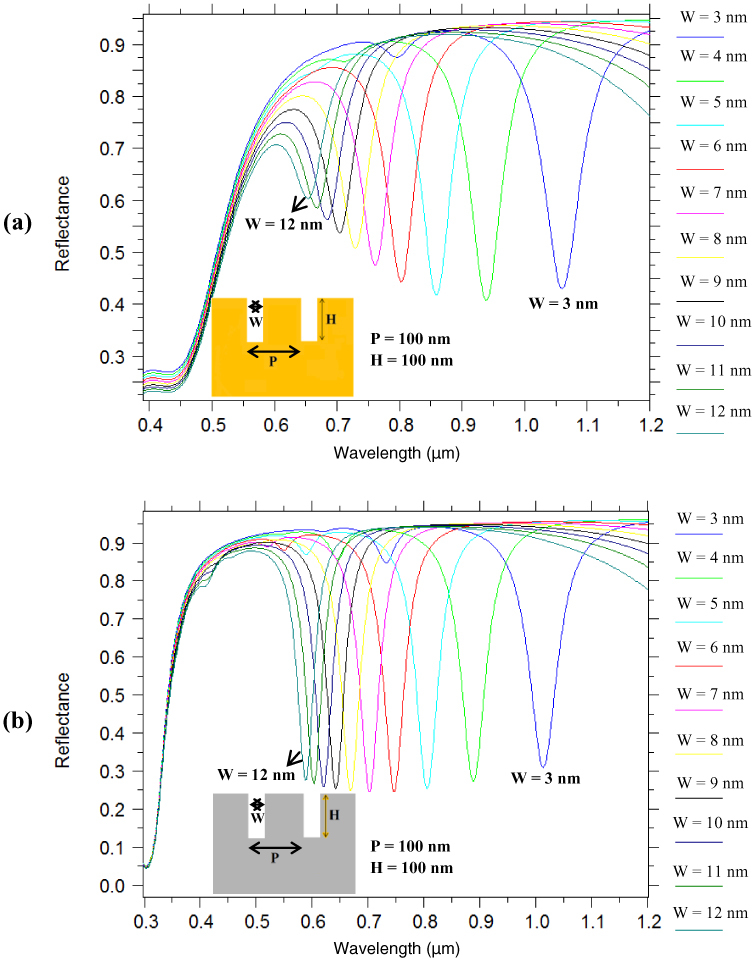
RCWA calculations showing the effect of nano-grating groove width ‘W’ on the plasmon resonance dips in the reflectance spectra for narrow groove metallic nano-gratings: (a) Gold nano-grating, and (b) Silver nano-grating. The nano-grating height ‘H’ and periodicity ‘P’ are 100 nm and the refractive index of the medium surrounding the nano-grating was 1.33.
The effect of periodicity of the plasmonic nano-gratings on the plasmonic band structure for gold nano-gratings is shown in Fig. 4 . One can observe in Fig. 4 that a plasmonic band associated with the main plasmon resonance related dip in the reflectance spectra is clearly visible along with some bands associated with the other plasmon resonance related dips. Figures 4a-4h show that the bands associated with the main plasmon resonance related dip in the reflectance spectra are clearly visible for the filling factors (filling factor F = W/P, where ‘W’ is the spacing between the adjacent nanolines in the plasmonic nano-grating and ‘P’ is the periodicity of the nano-grating) less than 0.10 but become less prominent as the filling factor is increased to 0.14. Moreover, the plasmon resonance band stretches to a periodicity of only 100 nm for ‘F’ values being above 0.10 (the value of nano-grating groove width ‘W’ for these parameters being 10 nm), highlighting the geometric parameters - periodicity ‘P’ of the nanolines in the nano-gratings and width ‘W’ of the gaps between these nanolines - are critical in determining whether the nano-gratings could be effectively employed for the development of SPR sensors. Similarly, the effect of periodicity on the plasmonic band structure for silver nano-gratings is shown in Fig. 5 . In Fig. 5, one also observes bands associated with the plasmon resonance related dips in the reflectance spectra and that the bands are more visible for the filling factors less than 0.20 but become less prominent for the filling factor values higher than 0.20. For filling factors as high as 0.08, the main plasmon resonance bands stretch to periodicities of 300 nm, indicating that nano-grating structures with 300 nm ‘P’ and 24 nm ‘W’ can also be feasibly employed for SPR sensing based on the narrow groove gratings.
Fig. 4.
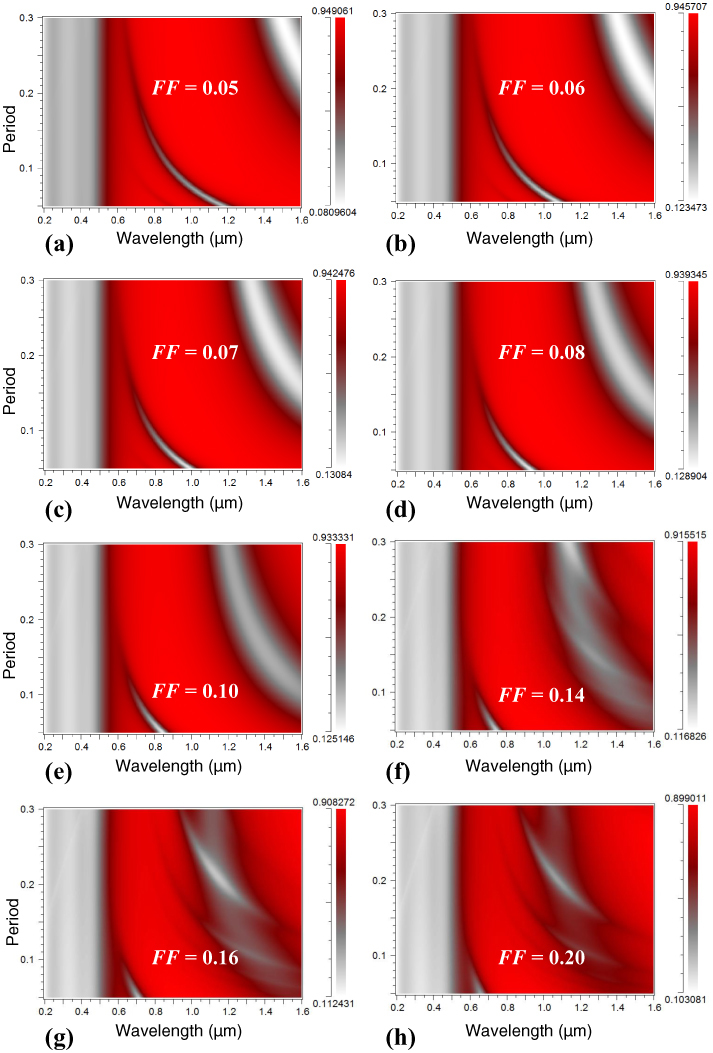
Effect of Periodicity ‘P’ of gold narrow groove plasmonic nano-grating structure on reflection spectra from the nano-gratings for different filling factors ‘FF’ of the nano-gratings: (a) 0.05, (b) 0.06, (c) 0.07, (d) 0.08, (e) 0.10, (f) 0.14, (g) 0.16, and (h) 0.2. In the calculations, the localized refractive index around the gold nano-gratings was taken as 1.53 (n=1.53 for 1 nm above the metallic film, the remaining region having n=1.33) and height ‘H’ was 100 nm.
Fig. 5.
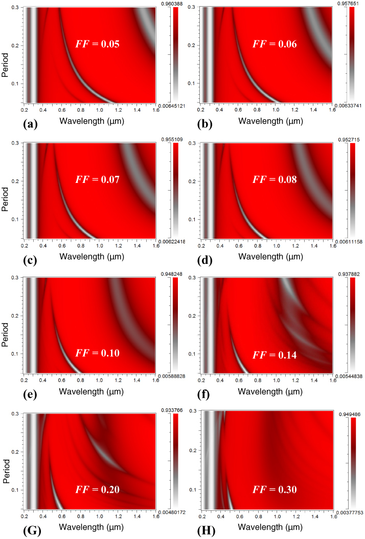
Effect of Periodicity ‘P’ of silver narrow groove plasmonic nano-grating structure on reflection spectra from the nano-gratings for different filling factors ‘FF’ of the nano-gratings: (a) 0.05, (b) 0.06, (c) 0.07, (d) 0.08, (e) 0.10, (f) 0.14, (g) 0.2, and (h) 0.3. In the calculations, the localized refractive index around the silver nano-gratings was taken as 1.53 (n=1.53 for 1 nm above the metallic film, the remaining region having n=1.33) and height ‘H’ was 100 nm.
While periodicity ‘P’ and groove widths ‘W’ have an effect on the plasmon resonance wavelengths associated with the nano-gratings, another critical parameter is the nano-grating height ‘H’ (See Fig. 1). Figures 6 and 7 provide RCWA calculations that show reflectance curves for narrow groove gold and silver nano-gratings as the height ‘H’ is varied from 50 nm to 250 nm, while the periodicity ‘P’ and the width ‘W’ between the nanolines in the nano-grating were 100 nm and 7 nm, respectively. For the calculations shown in Figs. 6-7, we selected the values of ‘P’ to be 100 nm as current deep UV lithography, focused ion beam milling, and electron beam lithography technologies allow the development of nanostructures with this periodicity; while the fabrication of sub-10 nm gaps (such as gaps ‘W’ being 7 nm) between the nanolines in the plasmonic nano-gratings could be carried out by employing other nanolithography processes that have been recently developed [49–54]. One can observe from Figs. 6a-6d and Figs. 7a-7d that as the height ‘H’ of the nano-gratings is increased from 50 nm to 250 nm, the number of plasmon resonance related dips in the reflection spectra increases. In the case of gold nano-gratings, there are one, one, three, four and five plasmon resonance related dips in the reflection spectra between 400 nm and 1600 nm when the values of ‘H’ are 50 nm, 100 nm, 150 nm, 200 nm, and 250 nm, respectively (See Fig. 6 and Fig. 2c). The different dips correspond to the different plasmon resonance modes (indicated as modes M1-M5 in Figs. 6 and 7) that are coupled into the metallic nano-gratings. Similarly, in the case of silver nano-gratings, the number of distinct plasmon resonance related dips between 400 nm and 1600 nm wavelengths are one, two, three, four, and five, respectively, when the values of ‘H’ are 50 nm, 100 nm, 150 nm, 200 nm, and 250 nm, respectively (See Fig. 7 and Fig. 2d). As Figs. 6-7 are plotted for wavelength values less than 1600 nm, mode 1 (M1) is not indicated in these figure as it occurs in the range of 2000 nm to 5000 nm for nano-grating height ‘H’ lying between 150 nm and 250 nm for Au nano-gratings, and for ‘H’ lying between 100 nm and 250 nm for Ag nano-gratings. The existence of multiple plasmon resonance dips in the reflection spectra indicates that the narrow groove plasmonic gratings can be used for SPR based sensing with light sources of different wavelengths corresponding to the dips in the reflection spectra. For example, the narrow groove silver nano-grating having ‘H’ as 150 nm (with ‘P’ and ‘W’ being 100 nm and 7 nm, respectively) has distinct dips at ~600 nm and ~900 nm and can be employed for surface plasmon resonance sensing using light sources (LEDs or lasers) having these wavelengths (See Fig. 7b). Figures 6 and 7 also show the differential reflectance signals for gold and silver nano-gratings, respectively, and enable us to determine the optimal value of ‘H’ that would lead to the highest differential reflectance signals. One can observe from Figs. 6a-6d and Fig. 2c that the narrow groove gold nano-grating - with 100 nm periodicity and 7 nm groove width - has the highest differential reflectance signal (greater than 0.4 or 40%) when ‘H’ is 150 nm. Similarly, one can observe from Figs. 7a-7d and Fig. 2d that the narrow groove silver nano-grating - with 100 nm periodicity and 7 nm groove width - has the highest differential reflectance signal (greater than 0.5 or 50%) when ‘H’ is 250 nm. The evolutions of the different plasmon resonance modes in gold and silver nano-gratings are shown in Fig. 6e and 7e, respectively. In Fig. 6e, the first plasmon resonance mode is coupled into the gold nano-grating even at very small values of ‘H’, and the maxima in this mode (M1) occurs at the value of ‘H’ of 15 nm. Similarly, in Fig. 7e, the first plasmon resonance mode (M1) for silver nano-gratings has a maxima occurring at the value of ‘H’ of 25 nm. From Figs. 6e and 7e, when the height of the gold and silver nano-gratings is increased, the number of modes increases and there are upto 5 modes for an ‘H’ value of 250 nm. From Fig. 6e, the amplitude of the differential reflectance is significantly greater for some plasmon modes coupled into the narrow groove gold nano-gratings such as Mode 2 (M2) for nano-grating heights ‘H’ greater than 75 nm and Mode 3 (M3) for nano-grating heights ‘H’ greater than 175 nm. Similarly, from Fig. 7e, the amplitude of the differential reflectance is greater for some plasmon modes coupled into the narrow groove silver nano-gratings such as Mode 2 (M2) for nano-grating heights ‘H’ greater than 75 nm and Mode 3 (M3) for nano-grating heights ‘H’ greater than ~190 nm. From Figs. 6 and 7, the sensitivity advantage (sensitivity is indicated by the amplitude of the differential reflectance before and after a localized change of refractive index in the vicinity of the nano-gratings, specifically 1 nm around the nano-grating surface) of employing narrow groove nano-gratings over continuous metallic films for modes 2, and 3 (M2-M3) is greater for gold nano-gratings as compared with silver nano-gratings - particularly for the case when the normalized value of the maximum amplitude of differential reflectance is calculated for the interrogation wavelengths less than 800 nm. This highlights the suitability of gold narrow groove nano-gratings for sensing localized changes in refractive index around the plasmonic nano-gratings. Moreover, the gold nano-gratings are expected to be chemically stable and would be ideal for developing plasmon resonance based sensing devices. Moreover, the plasmon mode M1 coupled into the narrow groove gratings provides significantly higher value of the amplitude of the differential reflectance as compared to the normalized value of the differential reflectance for a planar gold film (having an equivalent surface area as the nano-gratings) for ‘H’ values lying between 10 nm and 25 nm. This shows that the narrow groove nano-gratings with shallow depths (10-25 nm) can also be effectively employed for sensing of localized changes of refractive indices in the vicinity of the nano-gratings. Moreover, fabrication of shallow narrow groove (less than 25 nm) gold or silver nano-gratings via focused ion beam milling or other nanofabrication methods can be accomplished with more precision as compared to nano-gratings that are very deep (‘H’ being greater than 100 nm).
Fig. 6.
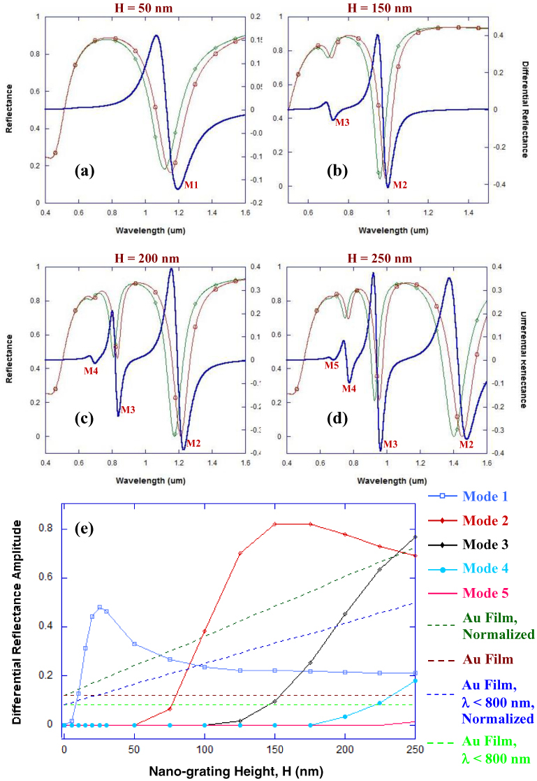
(a-d) RCWA calculations showing reflectance curves (differential reflectance in blue, reflectance curves with localized refractive index around the grating n = 1.33 in green and with n = 1.53 in red) for a narrow groove gold nano-grating - with 100 nm periodicity and 7 nm groove width - for a 1 nm binding of target (refractive index = 1.53) on the surface of the metallic film. The effect of nano-grating height ‘H’ on the reflection spectra is shown for the following values of ‘H’: (a) 50 nm, (b) 150 nm, (c) 200 nm, (d) 250 nm. (e) The effect of nano-grating height ‘H’ on the amplitude of the differential reflectance (peak maxima – peak minima) for different plasmon modes coupling into the narrow groove gold nano-gratings. The dashed red line provides the maximum value of the amplitude of differential reflectance for a planar gold film evaluated using the Kretschmann configuration and wavelength interrogation, while the dashed light green line provides the maximum value of the amplitude of differential reflectance for a planar gold film evaluated using the Kretschmann configuration when the interrogation wavelength is less than 800 nm. The dashed dark green line provides the maximum value of the amplitude of differential reflectance for a planar gold film - evaluated using Kretschmann configuration and employing wavelength interrogation - that is normalized such that the planar gold film would have the equivalent surface area as would be present in gold nano-gratings of height ‘H’, while the dashed blue line provides the normalized value of the maximum amplitude of differential reflectance when the wavelength of interrogation is less than 800 nm.
Fig. 7.
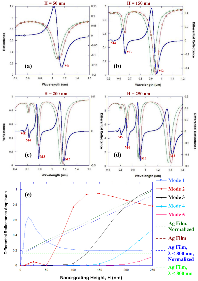
(a-d) RCWA calculations showing reflectance curves (differential reflectance in blue, reflectance curves with localized refractive index around the grating n = 1.33 in green and with n = 1.53 in red) for a narrow groove silver nano-grating - with 100 nm periodicity and 7 nm groove width - for a 1 nm binding of target (refractive index = 1.53) on the surface of the metallic film. The effect of nano-grating height ‘H’ on the reflection spectra is shown for the following values of ‘H’: (a) 50 nm, (b) 150 nm, (c) 200 nm, (d) 250 nm. (e) The effect of nano-grating height ‘H’ on the amplitude of the differential reflectance (peak maxima – peak minima) for different plasmon modes coupling into the narrow groove silver nano-gratings. The dashed red line provides the maximum value of the amplitude of differential reflectance for a planar silver film evaluated using the Kretschmann configuration and wavelength interrogation, while the dashed light green line provides the maximum value of the amplitude of differential reflectance for a planar silver film evaluated using the Kretschmann configuration when the interrogation wavelength is less than 800 nm. The dashed dark green line provides the maximum value of the amplitude of differential reflectance for a planar silver film - evaluated using Kretschmann configuration and employing wavelength interrogation - that is normalized such that the planar silver film would have the equivalent surface area as would be present in silver nano-gratings of height ‘H’, while the dashed blue line provides the normalized value of the maximum amplitude of differential reflectance when the wavelength of interrogation is less than 800 nm.
In this paper, we have also discussed how normally incident radiation can be coupled into surface plasmons using the narrow groove plasmonic nano-gratings. Figure 8a shows the angle dependence of the reflectance from gold and silver narrow groove nano-gratings when the incident radiation is at 761 nm for the gold nano-grating and 705 nm for the silver nano-grating corresponding to their plasmon resonance wavelengths at normal incidence, respectively. From Fig. 8a, between −60 and 60 degrees, although the maxima in the reflectance signals occurs for normal incidence of the radiation on the nano-gratings, angles that are not normal (say 15 degrees) can also be employed for the SPR sensing purposes. This could greatly facilitate the experimental setup for the SPR measurements and enable different beam directions for the incident and reflected beams. Figure 8b shows a comparison of RCWA calculations of reflectance spectra from nanolines grating structures of different materials, for normally incident radiation on these nano-gratings. Once can observe that the plasmon resonance related dips in the reflection spectra are only visible for plasmonic materials such as gold and silver and not for other materials such as silicon and silicon-dioxide or even non-plasmonic metals such as titanium. This provides further evidence of the role of surface plasmons in the coupling of radiation into the narrow groove nano-gratings.
Fig. 8.
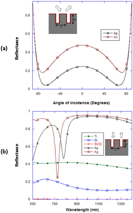
(a) RCWA calculations showing the effect of angle of incidence on reflectance - the wavelength of the incident radiation being the plasmon resonance wavelength for the gold (761 nm) and silver (702 nm) nanolines grating structures. The nano-grating height ‘H’ and periodicity ‘P’ are 100 nm, the spacing ‘W’ between the nanolines is 7 nm, and the refractive index of the medium surrounding the nano-grating is 1.33. (b) RCWA calculations showing the reflectance spectra from nanolines grating structures of different materials, for normally incident radiation on these nano-gratings. For all nano-grating materials, the nano-grating height ‘H’ and periodicity ‘P’ are 100 nm, the spacing ‘W’ between the nanolines is 7 nm, and the refractive index of the medium surrounding the nano-grating is 1.33.
Theoretical analysis of the enhancement of EM fields inside plasmonic narrow groove nano-gratings were previously described in literature [36, 37]. We carried out FDTD calculations to show the spatial distribution of the EM fields inside the narrow groove nano-gratings (See Fig. 9 ). Figure 9a shows the electric field enhancement when the gap between the adjacent nanolines of silver nano-gratings is 7 nm, the periodicity and the height of the narrow groove nano-grating being 100 nm. Similarly Fig. 9b shows the electric field enhancement for gold nano-gratings with a nanolines gap of 7 nm. From Figs. 9a-9b, the highest E-field enhancement is near the top of the nano-grating. As described earlier [36, 37], the coupling of the incident radiation to surface plasmons occurs primarily due to cavity modes inside the narrow slits. This leads to surface plasmons traveling in both directions along the inner metallic surfaces of the narrow groove in the grating. As the spacing between the adjacent nanolines of the nano-grating is reduced, coupling between the SPs traveling along the nanowire walls occurs which sets up standing waves (multiple standing surface plasmon polaritons modes are set up inside each groove) in the narrow groove nano-grating and high enhancement of EM fields in these gaps.
Fig. 9.
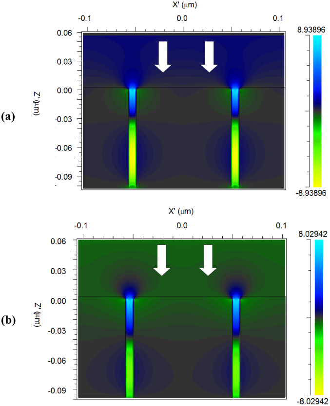
FDTD Simulations showing EM field enhancement (at plasmon resonance wavelengths) in the narrow gaps between neighboring nanolines of a nano- gratings having 100 nm Periodicity ‘P’ and Height ‘H’, and 7 nm gap between adjacent nanolines for: (a) Silver and (b) Gold nano-gratings. In these calculations, the direction of the TM radiation incident on the nano-gratings is the ‘Z’ direction.
Figure 10 shows the effect of varying the bulk refractive ‘n2’ on the plasmon resonance wavelength dip in the reflectance spectra for gold and silver narrow groove nano-gratings. The plasmon resonance wavelength red-shifts are observed on increasing the bulk refractive index from 1.33 to 1.4 for both gold and silver nano-gratings. The sensitivity to changes in the refractive index are calculated as ~500 nm/RIU in the case of gold narrow groove nano-gratings and ~450 nm/RIU in the case of silver narrow groove nano-gratings. These values of sensitivities to changes in bulk refractive indices are lower than that obtained from gold and silver continuous thin films evaluated by using the Kretschmann configuration. Lower sensitivity to changes in bulk refractive index implies that the narrow groove silver or gold nano-gratings - that are extremely sensitive to localized changes in the refractive index in the vicinity of the metal films of the nano-gratings - are more stable for use as biosensors as they will be affected less by the changes in bulk refractive index of the media surrounding the sensors, which could result from temperature variations.
Fig. 10.
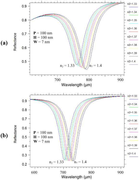
Reflectance spectra obtained from RCWA simulations showing the effect of varying the bulk refractive ‘n2’ on the plasmon resonance wavelength peak for (a) Au nano-grating and (b) Ag nano-grating, the periodicity ‘P’ and height ‘H’ being 100 nm and the spacing between the nanolines ‘W’ being 7 nm.
Finally, we optimize the values of periodicity ‘P’ of the nano-gratings as well as the groove width ‘W’ to determine the maximum possible value of differential reflectance signal upon binding of a 1 nm thick target (having a refractive index of 1.53) on the surface of the metallic film. The differential reflectance signals for gold nano-gratings, having ‘W’ values varying between 3 nm and 20 nm and ‘P’ values between 50 nm and 200 nm are shown in Fig. 11 . As discussed earlier in Figs. 6-7, the value of the amplitude of the differential reflectance can be significantly higher (for certain plasmon resonance modes coupled into the nano-gratings) than those for a planar gold film that is evaluated using the Kretschmann configuration and the wavelength interrogation method. In the plots of differential reflectance signals for different values of periodicities (shown in Figs. 11a-11d), one can observe an increase in the differential reflectance signals as the nano-grating groove width ‘W’ is reduced, especially when ‘W’ is reduced below 8 nm. The increase in differential reflectance signals (and therefore high sensitivity of the nano-gratings when employed as sensors) as ‘W’ is decreased, could be attributed to the increase in enhancement of electric fields inside the narrow groove nano-gratings with a decrease in the gap between the nanolines of the nano-gratings [36, 37]. Higher the values of EM fields inside the narrow grooves of the nano-gratings, greater shifts in the plasmon resonance wavelengths are expected when the localized refractive index - of the medium in the vicinity of the metal film forming the nano-grating - is changed. We observe from Figs. 11a that while the maximum possible value of differential reflectance signals (peak maxima) of 0.63 or 63% can be obtained from gold nano-gratings with a value of ‘W’ of 3 nm and a periodicity of 50 nm, Figs. 11b-d show that the maximum values of differential reflectance signals are ~0.44 or 44% when the periodicity is 100 nm while it is ~0.35 or 35% and ~0.29 or 29% when the periodicities are 150 nm and 200 nm respectively (for ‘W’ being 3 nm). Although the differential reflectance values for ‘W’ = 3nm provide an indication of the limit of the narrow groove sensors being described in this paper, this gap dimension is almost impossible to achieve by employing the current nanofabrication technologies. On the other hand, one can observe that the maximum values of differential reflectance signals are ~0.22 or 22% when the periodicity is 50 nm while it is ~0.17 or 17% when the periodicity is 100 nm for the value of ‘W’ = 7nm, a gap dimension that could possibly be realized considering some of the recent developments in nanofabrication methodologies.
Fig. 11.
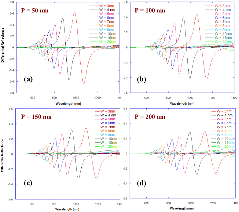
RCWA calculations showing differential reflectance curves for a change of the localized refractive index - 1 nm above the metallic film surface of a narrow groove gold nano-grating - from n = 1.33 to n = 1.53 upon binding of a 1nm thick target having a refractive index of 1.53 on the surface of the metallic film. The gold nano-grating had a 100 nm periodicity and the effect of nano-grating groove width ‘W’ on the differential reflectance spectra is shown for the following values of periodicity ‘P’: (a) 50 nm, (b) 100 nm, (c) 150 nm, (d) 200 nm.
Figure 12 shows the effect of groove width ‘W’ on the amplitude of the differential reflectance (peak maxima – peak minima) signals obtained from gold nano-gratings. From Fig. 11, there are several plasmon modes that are coupled into the narrow groove nano-gratings. In order to obtain the value of the amplitude of the differential reflectance that is plotted in Fig. 12, we selected the plasmon mode that had the highest value of the amplitude of the differential reflectance in the spectral region 450 nm-1600 nm - the region of interest for developing the surface plasmon sensors. The dashed lines provide the baseline value of the amplitude of differential reflectance for a planar gold film evaluated using the Kretschmann configuration and employing wavelength interrogation. In Fig. 12a the plasmon resonance related dips in the reflectance spectra (before and after the localized refractive index change) - as well as the maxima and the minima in the differential reflectance curves - are considered for wavelengths less than 1600 nm, while in Fig. 12b, the plasmon resonance related dips in the reflectance spectra are considered for wavelengths less than 800 nm. From a practical experimental standpoint, silicon photodetectors (spectrum wavelength range 190 - 1100 nm) can be employed for plasmon resonance peak measurements below 800 nm, while for measurements in the spectral region 800 nm-1600 nm, germanium or indium gallium arsenide photodetectors could be employed. From Fig. 12a, the value of the amplitude of the differential reflectance is higher for nano-gratings - having groove width ‘W’ below ~12.5 nm and having 'P' equal to 50 nm and 100 nm - than that obtained for a planar gold film evaluated using the Kretschmann configuration (not normalized). Similarly, from Fig. 12a, the value of the amplitude of the differential reflectance is higher for nano-gratings - having groove width ‘W’ below 10 nm and having 'P' equal to 150 nm and 200 nm - than that obtained for a planar gold film evaluated using the Kretschmann configuration (not normalized). Figure 12b shows the maximum value of the amplitude of the differential reflectance (for both nano-gratings and continuous thin films) when the plasmon resonance related dips in the reflectance spectra are considered for wavelengths less than 800 nm. We can observe from Fig. 12b that the value of the amplitude of the differential reflectance is higher for nano-gratings - having ‘W’ below 14 nm for 'P' equal to 50 nm and 100 nm, ‘W’ below 18 nm for 'P' equal to 150 nm, and ‘W’ below 20 nm for 'P' equal to 200 nm - than that obtained for a planar gold film evaluated using the Kretschmann configuration (not normalized). Moreover we can see from Fig. 12a that the value of the amplitude of the differential reflectance is higher for nano-gratings - having values of 'W' less than ~7 nm for 'P' equal to 50nm and 100 nm, 'W' less than 7.5 nm for 'P' equal to 150 nm, and 'W' less than 8 nm for 'P' equal to 200 nm - than that obtained for a planar gold film evaluated using the Kretschmann configuration that are normalized such that the surface area of the continuous gold film is equivalent to that of the nano-gratings. Hence, one can attribute the increase in the amplitude of differential reflectance signals as ‘W’ is decreased below 10 nm not just to an increase in the surface area (on developing a nano-grating on the plasmonic film) but also an increase in the EM fields inside the narrow grooves of the nano-gratings, when surface plasmon modes are coupled to the nano-gratings. Moreover we can see from Fig. 12b that the value of the amplitude of the differential reflectance is higher for nano-gratings - having values of 'W' less than ~7.5 nm for 'P' equal to 50 nm, 'W' less than 8.5 nm for 'P' equal to 100 nm, and 'W' less than 9 nm for 'P' equal to 150 nm and 200 nm - than that obtained for a planar gold film evaluated using the Kretschmann configuration that are normalized such that the surface area of the continuous gold film is equivalent to that of the nano-gratings.
Fig. 12.
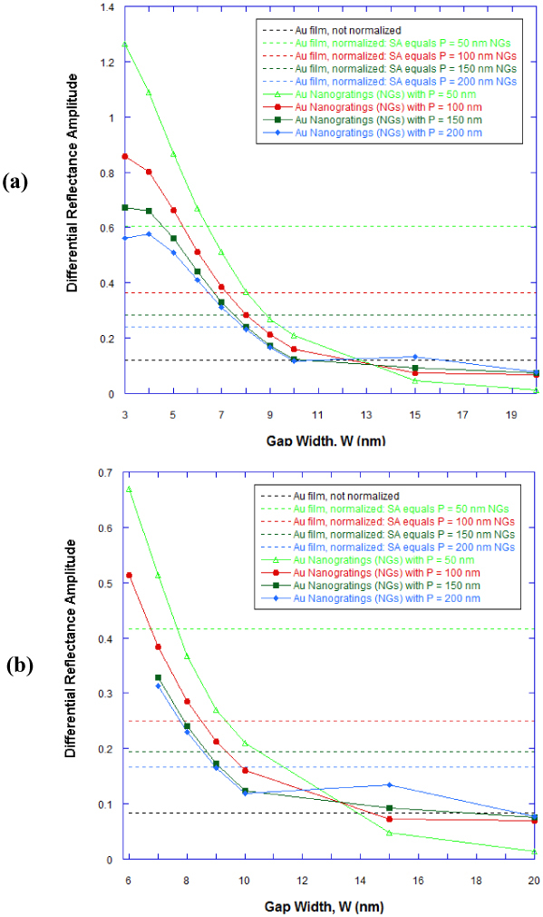
RCWA calculations showing the effect of groove width ‘W’ on the amplitude of the differential reflectance (peak maxima – peak minima) signals obtained from gold nano-gratings, when the plasmon resonance related dips in the reflectance spectra (before and after the localized refractive index change) - as well as the maxima and the minima in the differential reflectance curves - are considered (a) for wavelengths less than 1600 nm and (b) for wavelengths less than 800 nm. The gold nano-grating had a 100 nm periodicity and the effect of nano-grating groove width ‘W’ on the differential reflectance amplitude is plotted for different values of periodicity ‘P’: 50 nm (continuous light green line), 100 nm (continuous red line), 150 nm (continuous dark green line), and 200 nm (continuous blue line). The differential reflectance curves were obtained for a change of the localized refractive index - 1 nm above the metallic film surface of a narrow groove gold nano-grating - from n = 1.33 to n = 1.53 upon binding of a 1nm thick target having a refractive index of 1.53 on the surface of the metallic film. The dashed black line provides the baseline value of the amplitude of differential reflectance for a planar gold film evaluated using the Kretschmann configuration and employing wavelength interrogation. The other dashed lines provide the baseline values of the amplitude of differential reflectance for a planar gold film - evaluated using Kretschmann configuration and employing wavelength interrogation - that are normalized such that the planar gold film would have equivalent surface area as would be present in gold nano-gratings of groove periodicity ‘P’ when the value of ‘P’ is 50 nm (dashed light green line), 100 nm (dashed red line), 150 nm (dashed dark green line), and 200 nm (dashed blue line).
A trend similar to that shown in Fig. 11 is also observed in Figs. 13a -13d for silver nano-gratings. Similarly, we observe from Figs. 13a that while the maximum possible value of differential reflectance signal of ~0.75 or 75% can be obtained from silver nano-gratingswith a value of ‘W’ of 3 nm and a periodicity of 50 nm, Figs. 13b-d shows that the maximum values of differential reflectance signals are 0.57 or 57% (for ‘W’ being 3 nm, a gap dimension that is almost impossible to achieve by the current nanofabrication technologies) when the periodicity is 100 nm while it is ~0.47 or 47% and ~0.41 or 41% when the periodicities are 150 nm and 200 nm respectively. On the other hand we can observe from Fig. 13b that maximum values of differential reflectance signals above 0.25 or 25% can be obtained for silver nano-gratings (nano-grating ‘P’ and ‘H’ being 100 nm) having the value of ‘W’ being as high as 10 nm, while the maximum values of differential reflectance signals of ~0.16 or 16% can be obtained for the value of ‘W’ being as high as 15 nm – both values of ‘W’ (10 nm and 15 nm) are realizable due to the recent developments in nanofabrication.
Fig. 13.
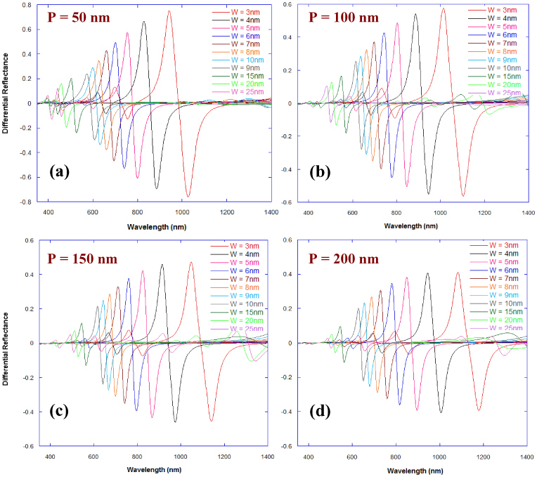
RCWA calculations showing differential reflectance curves for a change of the localized refractive index - 1 nm above the metallic film surface of a narrow groove silver nano-grating - from n = 1.33 to n = 1.53 upon binding of a 1 nm thick target having a refractive index of 1.53 on the surface of the metallic film. The silver nano-grating had a 100 nm periodicity and the effect of nano-grating groove width ‘W’ on the differential reflectance spectra is shown for the following values of periodicity ‘P’: (a) 50 nm, (b) 100 nm, (c) 150 nm, (d) 200 nm.
Figure 14 shows the effect of decreasing groove width ‘W’ on the increase in the amplitude of the differential reflectance (peak maxima – peak minima) signals obtained from silver nano-gratings. One can observe from Fig. 14a that the value of the amplitude of the differential reflectance is higher for nano-gratings - having groove width ‘W’ below 18 nm for 'P' lying between 50 and 200 nm - than that obtained for a planar silver film evaluated using the Kretschmann configuration (not normalized). Moreover, from Fig. 14a, the value of the amplitude of the differential reflectance is higher for nano-gratings - having 'W' less than 12 nm for 'P' equal to 200 nm, having 'W' less than 11.5 nm for 'P' equal to 150 nm, having 'W' less than 11 nm for 'P' equal to 100 nm, and having 'W' less than 7.5 nm for 'P' equal to 50 nm - than that obtained for a planar silver film evaluated using the Kretschmann configuration that are normalized such that the surface area of the continuous silver film is equivalent to that of the nano-gratings. From Figs. 12a and 14a, one can observe that the decrease in the differential reflectance signals as the value of ‘W’ is increased above 10 nm is greater in the case of gold nano-gratings as compared to silver nano-gratings. From Fig. 14b, the value of the amplitude of the differential reflectance is higher for nano-gratings - having groove width ‘W’ below 17 nm for 'P' lying between 50 and 200 nm - than that obtained for a planar silver film evaluated using the Kretschmann configuration (not normalized). Moreover, from Fig. 14b, the value of the amplitude of the differential reflectance is higher for nano-gratings - having 'W' less than 12.5 nm for 'P' equal to 200 nm, having 'W' less than 12 nm for 'P' equal to 150 nm and 100 nm, and having 'W' less than 7.5 nm for 'P' equal to 50 nm - than that obtained for a planar silver film evaluated using the Kretschmann configuration that are normalized such that the surface area of the continuous silver film is equivalent to that of the nano-gratings. These dimensions of nano-gratings gaps - especially gap dimensions in the range of 10-18 nm - and periodicities can be fabricated due to the advances in nano-lithography in the last few years [43–50]. For more sensitive sensors, sub-10 nm gaps between the nanolines in the plasmonic nano-gratings need to be fabricated. Their fabrication could be carried out by employing some these processes [49, 50] or other nanolithography processes that have been recently developed [51–54].
Fig. 14.
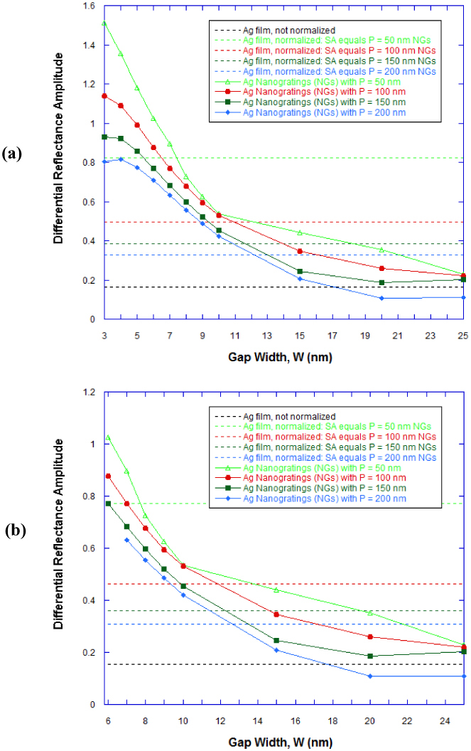
RCWA calculations showing the effect of groove width ‘W’ on the amplitude of the differential reflectance (peak maxima – peak minima) signals obtained from silver nano-gratings, when the plasmon resonance related dips in the reflectance spectra (before and after the localized refractive index change) - as well as the maxima and the minima in the differential reflectance curves - are considered (a) for wavelengths less than 1600 nm and (b) for wavelengths less than 800 nm. The silver nano-grating had a 100 nm periodicity and the effect of nano-grating groove width ‘W’ on the differential reflectance amplitude is plotted for different values of periodicity ‘P’: 50 nm (continuous light green line), 100 nm (continuous red line), 150 nm (continuous dark green line), and 200 nm (continuous blue line). The differential reflectance curves were obtained for a change of the localized refractive index - 1 nm above the metallic film surface of a narrow groove silver nano-grating - from n = 1.33 to n = 1.53 upon binding of a 1 nm thick target having a refractive index of 1.53 on the surface of the metallic film. The dashed black line provides the baseline value of the amplitude of differential reflectance for a planar silver film evaluated using the Kretschmann configuration and employing wavelength interrogation. The other dashed lines provide the baseline values of the amplitude of differential reflectance for a planar silver film - evaluated using Kretschmann configuration and employing wavelength interrogation - that are normalized such that the planar silver film would have equivalent surface area as would be present in silver nano-gratings of groove periodicity ‘P’ when the value of ‘P’ is 50 nm (dashed light green line), 100 nm (dashed red line), 150 nm (dashed dark green line), and 200 nm (dashed blue line).
The calculations described in this paper have shown that SPR sensing using narrow groove plasmonic nano-gratings cannot only enable direct coupling of normally incident light into surface plasmons, it can also lead to substantially higher differential reflectance signals - on localized change of refractive index in the narrow groove plasmonic gratings - as compared to those obtained from conventional SPR based sensing based on continuous metallic films and the Kretschmann configuration. These SPR sensors could be employed either as surface plasmon resonance sensors using the spectral interrogation method (for point measurements) or as surface plasmon resonance imaging (SPRI) sensors.
4. Conclusion
In this paper, we have described a novel surface plasmon resonance sensing configuration that is based on narrow groove plasmonic nano-grating structures. The gold and silver nano-gratings have nano-scale gaps, between the nanolines in the gratings, smaller than 15 nm and allow normally incident radiation to be coupled into surface plasmons without the use of the Kretschmann configuration. We employed Rigorous Coupled Wave Analysis (RCWA) calculations to study the effect of the nano-gratings’ parameters - such as periodicity, spacing between the nanolines, and the height of the nanolines - on their plasmon resonance wavelengths as well as to optimize these parameters to obtain the highest sensitivity of the nano-gratings to localized changes in refractive index when they are employed as SPR sensors. The RCWA calculations demonstrate that - even for grooves with small heights - much higher (several folds) values of differential reflectance signals are obtained from narrow groove plasmonic gratings as compared to those obtained from conventional SPR sensors that are based on planar plasmonic films and the Kretschmann configuration. The narrow groove nano-grating based SPR sensors would lead to the development of more robust SPR sensors as the coupling of normally incident radiation to surface plasmons eliminates the angular dependence requirements of SPR based sensing. Such narrow groove nano-grating based SPR sensors should find application for extremely sensitive detection of chemical and biological molecules based on surface plasmon resonance sensing and imaging.
Acknowledgements
The authors would like to thank the sponsors of this work - National Institutes of Health, USA (Grants R01 EB006201 and R01 ES014774) and CNRS, France. Institut d’Optique is part of the European Network of Excellence Photonics4Life, P4L, granted by the FP7 framework. Dr. Michael Canva also acknowledges partial financial support from the French DGA for his overseas sabbatical.
References and links
- 1.Homola J., Yee S. S., Gauglitz G., “Surface plasmon resonance sensors: Review,” Sens. Actuators B Chem. 54(1-2), 3–15 (1999). 10.1016/S0925-4005(98)00321-9 [DOI] [Google Scholar]
- 2.Jorgenson R. C., Yee S. S., “A fiber optic chemical sensor based on surface plasmon resonance,” Sens. Actuators B Chem. 12(3), 213–220 (1993). 10.1016/0925-4005(93)80021-3 [DOI] [Google Scholar]
- 3.J. Homola, Surface Plasmon Resonance Based Sensors (Springer, Berlin, 2006). [Google Scholar]
- 4.Čtyroký J., Homola J., Skalský M., “Tuning of spectral operation range of a waveguide surface plasmon resonance sensor,” Electron. Lett. 33(14), 1246–1248 (1997). 10.1049/el:19970814 [DOI] [Google Scholar]
- 5.Slavík R., Homola J., Čtyroký J., Brynda E., “Novel spectral fiber optic sensor based on surface plasmon resonance,” Sens. Actuators B Chem. 74(1-3), 106–111 (2001). 10.1016/S0925-4005(00)00718-8 [DOI] [Google Scholar]
- 6.Schuck P., “Use of surface plasmon resonance to probe the equilibrium and dynamic aspects of interactions between biological macromolecules,” Annu. Rev. Biophys. Biomol. Struct. 26(1), 541–566 (1997). 10.1146/annurev.biophys.26.1.541 [DOI] [PubMed] [Google Scholar]
- 7.Malmqvist M., “Surface plasmon resonance for detection and measurement of antibody-antigen affinity and kinetics,” Curr. Opin. Immunol. 5(2), 282–286 (1993). 10.1016/0952-7915(93)90019-O [DOI] [PubMed] [Google Scholar]
- 8.C. F. Bohren, and D. R. Huffman, Absorption and Scattering of Light by Small Particles (Wiley, New York 1983). [Google Scholar]
- 9.Haes A. J., Van Duyne R. P., “A nanoscale optical biosensor: sensitivity and selectivity of an approach based on the localized surface plasmon resonance spectroscopy of triangular silver nanoparticles,” J. Am. Chem. Soc. 124(35), 10596–10604 (2002). 10.1021/ja020393x [DOI] [PubMed] [Google Scholar]
- 10.Mock J. J., Smith D. R., Schultz S., “Local refractive index dependence of plasmon resonance spectra from individual nanoparticles,” Nano Lett. 3(4), 485–491 (2003). 10.1021/nl0340475 [DOI] [Google Scholar]
- 11.Futamata M., Maruyama Y., Ishikawa M., “Local electric field and scattering cross section of Ag nanoparticles under surface plasmon resonance by finite difference time domain method,” J. Phys. Chem. B 107(31), 7607–7617 (2003). 10.1021/jp022399e [DOI] [Google Scholar]
- 12.Dhawan A., Muth J. F., “Plasmon resonances of gold nanoparticles incorporated inside an optical fibre matrix,” Nanotechnology 17(10), 2504–2511 (2006). 10.1088/0957-4484/17/10/011 [DOI] [PubMed] [Google Scholar]
- 13.Otto A., Mrozek I., Grabhorn H., Akemann W., “Surface-enhanced Raman scattering,” J. Phys. Condens. Matter 4(5), 1143–1212 (1992). 10.1088/0953-8984/4/5/001 [DOI] [Google Scholar]
- 14.K. Kneipp, M. Moskovits, and H. Kneipp, Surface -Enhanced Raman Scattering: Physics and Applications, (Springer, Berlin, 2006). [Google Scholar]
- 15.Vo-Dinh T., ““Surface-enhanced Raman spectroscopy using metallic nanostructures,” Trends in Anal. Chem. 17, 557–582 (1998). 10.1016/S0165-9936(98)00069-7 [DOI] [Google Scholar]
- 16.Kerker M., “Electromagnetic model for surface-enhanced Raman scattering (SERS) on metal colloids,” Acc. Chem. Res. 17(8), 271–277 (1984). 10.1021/ar00104a002 [DOI] [Google Scholar]
- 17.R. K. Chang, and T. E. Furtak, eds., Surface-Enhanced Raman Scattering (Plenum, New York, 1982). [Google Scholar]
- 18.Nelson B. P., Grimsrud T. E., Liles M. R., Goodman R. M., Corn R. M., “Surface plasmon resonance imaging measurements of DNA and RNA hybridization adsorption onto DNA microarrays,” Anal. Chem. 73(1), 1–7 (2001). 10.1021/ac0010431 [DOI] [PubMed] [Google Scholar]
- 19.Nakkach M., Lecaruyer P., Bardin F., Sakly J., Lakhdar Z. B., Canva M., “Absorption and related optical dispersion effects on the spectral response of a surface plasmon resonance sensor,” Appl. Opt. 47(33), 6177–6182 (2008). 10.1364/AO.47.006177 [DOI] [PubMed] [Google Scholar]
- 20.Bardin F., Bellemain A., Roger G., Canva M., “Surface plasmon resonance spectro-imaging sensor for biomolecular surface interaction characterization,” Biosens. Bioelectron. 24(7), 2100–2105 (2009). 10.1016/j.bios.2008.10.023 [DOI] [PubMed] [Google Scholar]
- 21.Piliarik M., Homola J., “Surface plasmon resonance (SPR) sensors: approaching their limits?” Opt. Express 17(19), 16505–16517 (2009). 10.1364/OE.17.016505 [DOI] [PubMed] [Google Scholar]
- 22.Kim K., Yoon S. J., Kim D., “Nanowire-based enhancement of localized surface plasmon resonance for highly sensitive detection: a theoretical study,” Opt. Express 14(25), 12419–12431 (2006). 10.1364/OE.14.012419 [DOI] [PubMed] [Google Scholar]
- 23.Byun K. M., Shuler M. L., Kim S. J., Yoon S. J., Kim D., “Sensitivity enhancement of surface plasmon resonance imaging using periodic metallic nanowires,” IEEE J. Lightwave Technol. 26(11), 1472–1478 (2008). 10.1109/JLT.2008.922182 [DOI] [Google Scholar]
- 24.Live L. S., Bolduc O. R., Masson J.-F., “Propagating surface plasmon resonance on microhole arrays,” Anal. Chem. 82(9), 3780–3787 (2010). 10.1021/ac100177j [DOI] [PubMed] [Google Scholar]
- 25.Malic L., Cui B., Veres T., Tabrizian M., “Enhanced surface plasmon resonance imaging detection of DNA hybridization on periodic gold nanoposts,” Opt. Lett. 32(21), 3092–3094 (2007). 10.1364/OL.32.003092 [DOI] [PubMed] [Google Scholar]
- 26.Ebbesen T. W., Lezec H. J., Ghaemi H. F., Thio T., Wolff P. A., “Extraordinary optical transmission through sub?wavelength hole arrays,” Nature 391, 667-669 (1998). 10.1038/35570 [DOI] [Google Scholar]
- 27.Dhawan A., Gerhold M. D., Muth J. F., “Plasmonic Structures based on Sub-Wavelength Apertures for Chemical and Biological Sensing Applications,” IEEE Sens. J. 8, 942-950 (2008). 10.1109/JSEN.2008.923933 [DOI] [Google Scholar]
- 28.Brolo A. G., Gordon R., Leathem B., Kavanagh K. L., “Surface plasmon sensor based on the enhanced light transmission through arrays of nanoholes in gold films,” Langmuir 20(12), 4813–4815 (2004). 10.1021/la0493621 [DOI] [PubMed] [Google Scholar]
- 29.De Leebeeck A., Kumar L. K. S., de Lange V., Sinton D., Gordon R., Brolo A. G., “On-chip surface-based detection with nanohole arrays,” Anal. Chem. 79(11), 4094–4100 (2007). 10.1021/ac070001a [DOI] [PubMed] [Google Scholar]
- 30.Lindquist N. C., Lesuffleur A., Im H., Oh S.-H., “Sub-micron resolution surface plasmon resonance imaging enabled by nanohole arrays with surrounding Bragg mirrors for enhanced sensitivity and isolation,” Lab Chip 9(3), 382–387 (2009). 10.1039/b816735d [DOI] [PubMed] [Google Scholar]
- 31.Zheng G., Cui X., Yang C., “Surface-wave-enabled darkfield aperture for background suppression during weak signal detection,” Proc. Natl. Acad. Sci. U.S.A. 107(20), 9043–9048 (2010). 10.1073/pnas.0912563107 [DOI] [PMC free article] [PubMed] [Google Scholar]
- 32.Lezec H. J., Thio T., “Diffracted evanescent wave model for enhanced and suppressed optical transmission through subwavelength hole arrays,” Opt. Express 12(16), 3629–3651 (2004). 10.1364/OPEX.12.003629 [DOI] [PubMed] [Google Scholar]
- 33.Degiron A.,“The role of localized surface plasmon modes in the enhanced transmission of periodic subwavelength apertures,” J. Opt. A, Pure Appl. Opt. 7(2), S90–S96 (2005). 10.1088/1464-4258/7/2/012 [DOI] [Google Scholar]
- 34.Wirgin A., and Lopez-Rios T., “Can surface-enhanced Raman scattering be caused by waveguide resonances?” Opt. Commun. 48(6), 416–420 (1984). 10.1016/0030-4018(84)90036-1 [DOI] [Google Scholar]
- 35.Tan W. C., Preist T. W., Sambles J. R., Wanstall N. P., “Flat surface-plasmon-polariton bands and resonant optical absorption on short-pitch metal Gratings,” Phys. Rev. 59, 12661–12666 (1999). 10.1103/PhysRevB.59.12661 [DOI] [Google Scholar]
- 36.García-Vidal F. J., Martın-Moreno L., “Transmission and focusing of light in one-dimensional periodically nanostructured metals,” Phys. Rev. B 66(15), 155412 (2002). 10.1103/PhysRevB.66.155412 [DOI] [Google Scholar]
- 37.Porto J. A., García-Vidal F. J., Pendry J. B., “Transmission Resonances on Metallic Gratings with Very Narrow Slits,” Phys. Rev. Lett. 83(14), 2845–2848 (1999). 10.1103/PhysRevLett.83.2845 [DOI] [Google Scholar]
- 38.López-Rios T., Mendoza D., García-Vidal F. J., Sánchez-Dehesa J., Pannetier B., “Surface Shape Resonances in Lamellar Metallic Gratings,” Phys. Rev. Lett. 81(3), 665–668 (1998). 10.1103/PhysRevLett.81.665 [DOI] [Google Scholar]
- 39.Hooper I. R., Sambles J. R., “Surface plasmon polaritons on narrow-ridged short-pitch metal gratings,” Phys. Rev. B 66(20), 205408 (2002). 10.1103/PhysRevB.66.205408 [DOI] [PubMed] [Google Scholar]
- 40.Garcia-Vidal F. J., Sanchez-Dehesa J., Dechelette A., Bustarret E., Lopez-Rios T., Fournier T., Pannetier B., “Localized surface plasmons in lamellar metallic gratings,” J. Lightwave Technol. 17(11), 2191–2195 (1999). 10.1109/50.803010 [DOI] [Google Scholar]
- 41.Lopez-Rios T., Wirgin A., “Role of waveguide and surface plasmon resonances in surface-enhanced Raman scattering at coldly evaporated metallic films,” Solid State Commun. 52(2), 197–201 (1984). 10.1016/0038-1098(84)90626-4 [DOI] [Google Scholar]
- 42.Lochbilher H., “Surface Polaritons on gold-wire Gratings,” Phys. Rev. B 50(7), 4795–4801 (1994). 10.1103/PhysRevB.50.4795 [DOI] [PubMed] [Google Scholar]
- 43.Aćimović S. S., Kreuzer M. P., González M. U., Quidant R., “Plasmon near-field coupling in metal dimers as a step toward single-molecule sensing,” ACS Nano 3(5), 1231–1237 (2009). 10.1021/nn900102j [DOI] [PubMed] [Google Scholar]
- 44.Fromm D. P., Sundaramurthy A., Schuck P. J., Kino G., Moerner W. E., “Gap-Dependent Optical Coupling of Single “Bowtie” Nanoantennas Resonant in the Visible,” Nano Lett. 4(5), 957–961 (2004). 10.1021/nl049951r [DOI] [Google Scholar]
- 45.Li S., Pedano M. L., Chang S. H., Mirkin C. A., Schatz G. C., “Gap structure effects on surface-enhanced Raman scattering intensities for gold gapped rods,” Nano Lett. 10(5), 1722–1727 (2010). 10.1021/nl100099g [DOI] [PubMed] [Google Scholar]
- 46.Dhawan A., Gerhold M. D., Vo-Dinh T., “Theoretical Simulation and Focused Ion Beam Fabrication of Gold Nanostructures For Surface-Enhanced Raman Scattering (SERS),” Nanobiotechnol. 3(3-4), 1–8 (2007). 10.1007/s12030-008-9017-x [DOI] [PMC free article] [PubMed] [Google Scholar]
- 47.Dhawan A., Muth J. F., Leonard D. N., Gerhold M. D., Gleeson J., Vo-Dinh T., Russell P. E., “Focused in beam fabrication of metallic nanostructures on end faces of optical fibers for chemical sensing applications,” J. Vac. Sci. Technol. B 26(6), 2168 (2008). 10.1116/1.3013329 [DOI] [PMC free article] [PubMed] [Google Scholar]
- 48.Leen J. B., Hansen P., Cheng Y.-T., Hesselink L., “Improved focused ion beam fabrication of near-field apertures using a silicon nitride membrane,” Opt. Lett. 33(23), 2827–2829 (2008). 10.1364/OL.33.002827 [DOI] [PubMed] [Google Scholar]
- 49.Im H., Bantz K. C., Lindquist N. C., Haynes C. L., Oh S.-H., “Vertically oriented sub-10-nm plasmonic nanogap arrays,” Nano Lett. 10(6), 2231–2236 (2010). 10.1021/nl1012085 [DOI] [PubMed] [Google Scholar]
- 50.Fischbein M. D., Drndić M., “Sub-10 nm device fabrication in a transmission electron microscope,” Nano Lett. 7(5), 1329–1337 (2007). 10.1021/nl0703626 [DOI] [PubMed] [Google Scholar]
- 51.Banholzer M. J., Qin L., Millstone J. E., Osberg K. D., Mirkin C. A., “On-wire lithography: synthesis, encoding and biological applications,” Nat. Protoc. 4(6), 838–848 (2009). 10.1038/nprot.2009.52 [DOI] [PMC free article] [PubMed] [Google Scholar]
- 52.Gnanavel T., Saghi Z., Yajid M. A. M., Peng Y., Inkson B. J., Gibbs M. R. J., Möbus G., “Nanoscale sculpting of ferromagnetic structures by electron beam ablation,” J. Phys.: Conference Series 241, 012075 (2010). 10.1088/1742-6596/241/1/012075 [DOI] [Google Scholar]
- 53.Auzelyte V., Dais C., Farquet P., Grützmacher D., Heyderman L. J., Luo F., Olliges S., Padeste C., Sahoo P. K., Thomson T., Turchanin A., David C., Solak H. H., “Extreme ultraviolet interference lithography at the Paul Scherrer Institut,” J. Micro/Nanolith. 8(2), 021204 (2009). 10.1117/1.3116559 [DOI] [Google Scholar]
- 54.Bezryadin A., Dekker C., “Nanofabrication of electrodes with sub-5 nm spacing for transport experiments on single molecules and metal clusters,” J. Vac. Sci. Technol. B 15(4), 793–799 (1997). 10.1116/1.589411 [DOI] [Google Scholar]
- 55.Gates B. D., Xu Q., Stewart M., Ryan D., Willson C. G., Whitesides G. M., “New approaches to nanofabrication: molding, printing, and other techniques,” Chem. Rev. 105(4), 1171–1196 (2005). 10.1021/cr030076o [DOI] [PubMed] [Google Scholar]
- 56.Moharam M. G., Gaylord T. K., “Three-dimensional vector coupled-wave analysis of planar-grating diffraction,” J. Opt. Soc. Am. 73(9), 1105–1112 (1983). 10.1364/JOSA.73.001105 [DOI] [Google Scholar]
- 57.Moharam M. G., Gaylord T. K., “Rigorous coupled-wave analysis of metallic surface-relief gratings,” J. Opt. Soc. Am. A 3(11), 780–787 (1986). 10.1364/JOSAA.3.001780 [DOI] [Google Scholar]
- 58.Byun K. M., Kim S. J., Kim D., “Design study of highly sensitive nanowire-enhanced surface plasmon resonance biosensors using rigorous coupled wave analysis,” Opt. Express 13(10), 3737–3742 (2005). 10.1364/OPEX.13.003737 [DOI] [PubMed] [Google Scholar]
- 59.Dhawan A., Norton S. J., Gerhold M. D., Vo-Dinh T., “Comparison of FDTD numerical computations and analytical multipole expansion method for plasmonics-active nanosphere dimers,” Opt. Express 17(12), 9688–9703 (2009). 10.1364/OE.17.009688 [DOI] [PubMed] [Google Scholar]
- 60.A. Taflove, and S. C. Hagness, Computational Electrodynamics: The Finite-Difference Time Domain Method; 2nd ed. (Artech, Boston, MA, 2000). [Google Scholar]


