Abstract
The development of hybrid electronic devices relies in large part on the integration of (bio)organic materials and inorganic semiconductors through a stable interface that permits efficient electron transport and protects underlying substrates from oxidative degradation. Group IV semiconductors can be effectively protected with highly-ordered self-assembled monolayers (SAMs) composed of simple alkyl chains that act as impervious barriers to both organic and aqueous solutions. Simple alkyl SAMs, however, are inert and not amenable to traditional patterning techniques. The motivation for immobilizing organic molecular systems on semiconductors is to impart new functionality to the surface that can provide optical, electronic, and mechanical function, as well as chemical and biological activity.
Microcontact printing (μCP) is a soft-lithographic technique for patterning SAMs on myriad surfaces.1-9 Despite its simplicity and versatility, the approach has been largely limited to noble metal surfaces and has not been well developed for pattern transfer to technologically important substrates such as oxide-free silicon and germanium. Furthermore, because this technique relies on the ink diffusion to transfer pattern from the elastomer to substrate, the resolution of such traditional printing is essentially limited to near 1 μm.10-16
In contrast to traditional printing, inkless μCP patterning relies on a specific reaction between a surface-immobilized substrate and a stamp-bound catalyst. Because the technique does not rely on diffusive SAM formation, it significantly expands the diversity of patternable surfaces. In addition, the inkless technique obviates the feature size limitations imposed by molecular diffusion, facilitating replication of very small (<200 nm) features.17-23 However, up till now, inkless μCP has been mainly used for patterning relatively disordered molecular systems, which do not protect underlying surfaces from degradation.
Here, we report a simple, reliable high-throughput method for patterning passivated silicon and germanium with reactive organic monolayers and demonstrate selective functionalization of the patterned substrates with both small molecules and proteins. The technique utilizes a preformed NHS-reactive bilayered system on oxide-free silicon and germanium. The NHS moiety is hydrolyzed in a pattern-specific manner with a sulfonic acid-modified acrylate stamp to produce chemically distinct patterns of NHS-activated and free carboxylic acids. A significant limitation to the resolution of many μCP techniques is the use of PDMS material which lacks the mechanical rigidity necessary for high fidelity transfer. To alleviate this limitation we utilized a polyurethane acrylate polymer, a relatively rigid material that can be easily functionalized with different organic moieties. Our patterning approach completely protects both silicon and germanium from chemical oxidation, provides precise control over the shape and size of the patterned features, and gives ready access to chemically discriminated patterns that can be further functionalized with both organic and biological molecules. The approach is general and applicable to other technologically-relevant surfaces.
Keywords: Bioengineering, Issue 58, Soft lithography, microcontact printing, protein arrays, catalytic printing, oxide-free silicon
Protocol
1A. Primary Monolayer Formation on Silicon
Cut silicon wafer into 1cm2 substrates, dust and rinse with water and filtered ethanol.
Remove organic contamination by submerging the silicon substrates in a glass dish containing Nano strip at 75ºC. After 15 minutes, rinse each substrate with deionized, filtered water.
Place each substrate in a 5% HF solution (Warning: HF is an extremely dangerous material) to remove the native oxide layer. After 5 minutes dry the oxide-free silicon with nitrogen
To produce a chlorinated substrate, immediately submerge each oxide-free silicon piece in a scintillation vial containing 2 ml of saturated PCl5 in chlorobenzene. This solution should be filtered to 0.2 μm.
Assemble a vial condenser on top of each vial and place them in a heatblock set to 112°C for one hour.
After reaction is complete, let vials cool and rinse each surface with chlorobenzene and dry under filtered nitrogen.
To form a propenyl-terminates substrate, place each chlorinated silicon surface in a pressure vial containing 4 ml of propenyl magnesium chloride. Place each pressure vial in a heatblock at 130 °C for 24 hours.
Take each pressure vial out of the heatblock and let cool.
Rinse each surface quickly with DCM and ethanol and dry under filtered nitrogen.
1B. Primary Monolayer Formation on Germanium
Cut germanium wafer into 1cm2 substrates, dust and rinse with water and filtered ethanol.
Remove organic contamination by submerging the surfaces in a glass dish containing acetone for 20 minutes
Place each surface in a 10% HCl solution for 15 minutes. This process simultaneously removes the native oxide layer and chlorinates the surface. After 5 minutes dry the substrates with nitrogen.
To form an octyl-terminated substrate, place each chlorinated germanium surface in a pressure vial containing 4 ml of octyl magnesium chloride (2 mM). Place each pressure vial in a heatblock at 130 °C for 48 hours.
Take each pressure vial out of the heatblock and let cool to room temperature.
Rinse each surface quickly with DCM and ethanol and dry under filtered nitrogen.
2. NHS Substrate Functionalization on Silicon and Germanium
Prepare a filtered 0.1 M NHS-diazirine solution in carbon tetrachloride. Warning: Keep light exposure to a minimum.
Pipet a few drops of the solution onto the methyl terminated surfaces. Allow solution to spread across the entire surface.
Place the surfaces under a UV lamp (☐=254 nm, 4400/cm2 at 0.74 inches). Allow the surfaces to react under UV light for 30 minutes, then add more NHS-diazirine to the surface and let the reaction proceed for an additional 30 minutes.
Rinse the NHS modified surfaces with DCM and ethanol and dry under filtered nitrogen.
3. Small Molecule Functionalization
React NHS-modified substrates in a 20 mM tert-butyl carbamoyl (Boc-) ethylenediamine solution in dichloromethane (DCM) for two hours at room temperature.
After the reaction, rinse the Boc-modified substrate with DCM and ethanol.
Deprotect the Boc modified substrate using 25% trifluoroacetic acid (TFA) in DCM for one hour at room temperature.
Rinse the resulting surface with DCM, ethanol and 10% (w/v) potassium bicarbonate in water and dry under filtered nitrogen.
Analyze all surfaces by XPS to determine the elemental composition.
4. Acidic Polyurethane Acrylate Stamp (PUA) Preparation
Dilute acrylate A by 30% with trimethylolpropane ethoxylate triacrylate B to reduce viscosity. Add photoinitiators C and D to the reaction mixture (Figure 6).
Add sodium 2-mercaptoethanesulfonate (0.2 g, 1.22 mmol) to a 4N HCl solution in dioxane (10 ml) and stir at room temperature for 2 minutes.
Filter off the sodium chloride first through a fine glass filter and then through a 0.2 μm PTFE membrane syringe filter to afford a clear solution of 2-mercaptoethanesulfonic acid in dioxane.
Evaporate dioxane under reduced pressure
React the resulting sulfonic acid with 2 ml of the polyurethane-acrylate prepolymeric mixture at room temperature and then under vacuum at 50 °C. Be sure to completely free the mixture from trapped air bubbles.
Cool the resulting solution to room temperature and polymerize between two glass microscope slides or a glass slide and a master by exposure to UV light for 2 hours at room temperature.
After polymerization, carefully peel the stamp off the master and wash the stamp with ethanol and water and dry with filtered nitrogen.
5. Catalytic Printing and SEM/AFM Analysis
Place the corresponding polyurethane-acrylate stamp on top of the NHS-modified substrate at room temperature for one minute with no external load to hold them together.
After the reaction, separate the stamp and substrate.
Rinse the substrate with ethanol, water, and ethanol then dry with filtered nitrogen.
Rinse the stamp with ethanol, water, and ethanol then dry with filtered nitrogen.
Keep stamps at room temperature before the next application.
Analyze the produced pattern using contact mode lateral atomic force microsopy (AFM) and scanning electron microscopy (SEM)
6. Protein Patterning and Fluorescent Microscopy
Submerge the NHS-patterned bifunctional substrate in Lysine-N,N-diacetic acid (20 mM) and Et3N (100 mM) in DMF:H20 (1:1) at room temperature for 1 hr and then rinsed with water and ethanol.
Incubate the substrates in a 50 mM NiSO4 solution for 5 min at room temperature.
Rinse the chelated substrates excessively with water and binding buffer (20 mM NaP, 250 mM NaCl, 10mM imidazole, pH 7.5) and submerge in a filtered GFP solution (˜40 μM) for 1 hr at 0°C.
Immediately rinse the substrates with binding buffer followed by PBS (pH 7.4).
Keep substrates hydrated in PBS at 0°C until they were ready for fluorescence microscopy analysis.
7. Protein Patterning and Fluorescent Microscopy
Submerge the NHS-patterned bifunctional substrate in Lysine-N,N-diacetic acid (20 mM) and Et3N (100 mM) in DMF:H20 (1:1) at room temperature for 1 hr and then rinsed with water and ethanol.
Incubate the substrates in a 50 mM NiSO4 solution for 5 min at room temperature.
Rinse the chelated substrates excessively with water and binding buffer (20 mM NaP, 250 mM NaCl, 10mM imidazole, pH 7.5) and submerge in a filtered GFP solution (˜40 μM) for 1 hr at 0°C.
Immediately rinse the substrates with binding buffer followed by PBS (pH 7.4).
Keep substrates hydrated in PBS at 0°C until they were ready for fluorescence microscopy analysis.
8. Representative Results:
An example of soft-lithographic catalytic nano patterning is shown in Figure 7. The approach creates chemoselective patterns on oxide-free silicon and germanium, which can be orthogonally functionalized with dissimilar chemical and biological moieties. The reaction between the NHS-functioanlized substrate and the catalytic patterned stamp leads to the hydrolysis of NHS moieties in areas of conformal contact, yielding a patterned bifunctional substrate bearing regions of NHS activated and free carboxylic acids. Due to the diffusion free nature of our method, we achieve resolution close to that of photolithography. For example, Figure 7 shows 125 nm features, which were uniformly reproduced across the entire silicon substrate surface. Remarkably, the catalytic stamp can be reused multiple times without losing efficiency.
Chemoselective functionalization of patterned semiconductors with biomolecules opens up the prospect of integrating traditional electronic materials with highly selective biological substrates for applications in sensing, diagnostic, and analytical areas of research. An example of such functionalization is shown in Figure 8, where NHS-patterned silicon was selectively functionalized with protein molecules. By exploiting the differential reactivities of activated and free carboxylic acids, we first affixed nitrilotriacetic acid-terminated (NTA) heterobifunctional linkers to the NHS-functionalized regions, and then used the resulting NTA-patterned surface as a template for the selective attachment of hexa-histidine-tagged GFP. Figure 8b clearly shows differential fluorescence intensity between GFP-modified and hydrolyzed free carboxylic acid regions. The size and shape of the replicated features are consistent between both NHS patterned surface (Figure 8a) and GFP-modified surface (Figure 8b), confirming the remarkable stability of carbon-passivated surfaces and the selectivity of the stamping approach. The protocol is not limited to His-tagged protein, and can be used to pattern other biomolecules including DNA and antibodies.
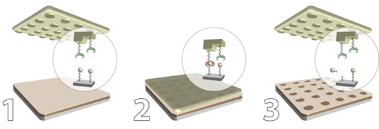 Figure 1. General scheme representing catalytic microcontact printing
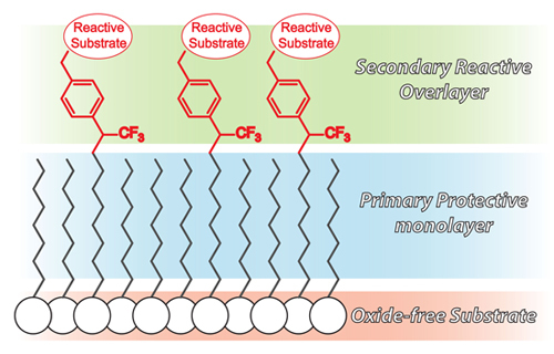 Figure 2. Structure of bi-layered molecular system on Ge and Si. Primary alkyl monolayer forms stable Ge-C or Si-C bonds with the substrate and provides a chemically inert and close packed system that protects the underlying surface from degradation.(b) Secondary overlayer forms stable C-C bonds with primary protective layer and provides terminal functional groups
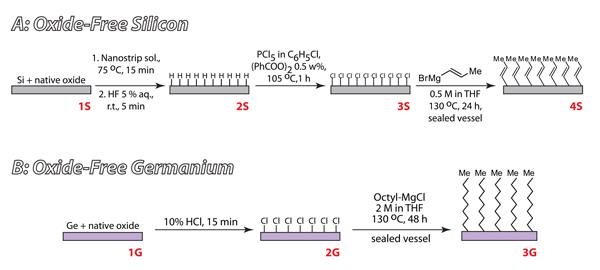 Figure 3. Reaction schemes representing formation of primary protective monolayers on Si (A) and Ge (B)
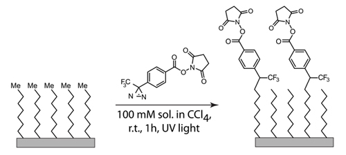 Figure 4. Chemical functionalization of the primary protective monolayer with a heterobifunctional carbene donor
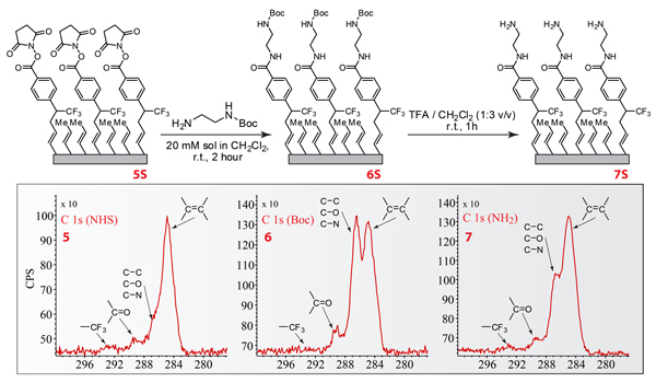 Figure 5. Reaction scheme demonstrating small molecule modifications of NHS-functionalized substrates and the corresponding XPS spectra
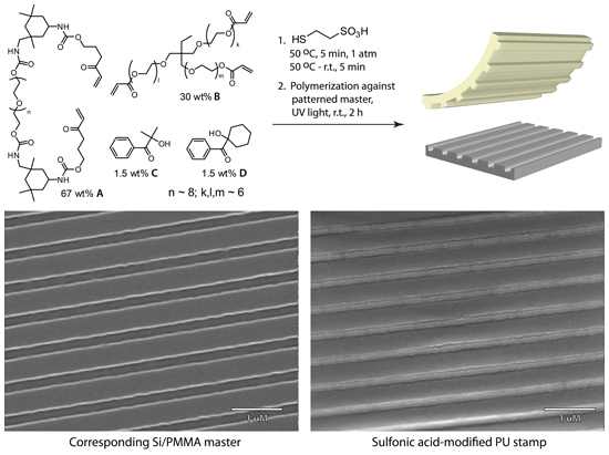 Figure 6. Composition of the catalytic pre-polymeric mixture, polymerization conditions, and SEM images of the patterned sulfonic acid-modified stamp and the corresponding PMMA-Si master
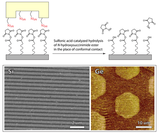 Figure 7. SEM and AFM friction images of patterned SAMs on Si and Ge with an acidic stamp
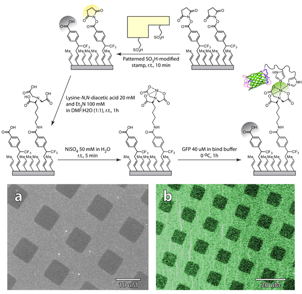 Figure 8. Soft-lithographic patterning and functionalization of passivated silicon with organic and biological molecules. a: SEM image of the patterned NHS-modified substrate. b: Fluorescent micrograph of GFP modified substrate.
Discussion
The presented protocol is a form or of inkless microcontact printing that can be universally applied to any substrate capable of supporting simple well-ordered monolayers. In this method, a stamp-immobilized catalyst transfers a pattern to a surface bearing corresponding functional groups. Because the process does not rely on ink transfer from stamp to surface the diffusive resolution limitation of traditional and reactive μCP is obviated, permitting routine manufacturing of nanoscale objects. The incorporation of a primary highly-ordered molecular system provides complete protection of the underlying semiconductor from oxidation damage. At the same time, the method supports immobilization of bulky reactive groups by utilizing a secondary reactive overlayer; together the system achieves both protection and functionalization.
The technique begins with the formation of stable carbon-surface bonds allowing for chemically inert primary monolayer which serves as an effective barrier to oxide formation. Formation of a secondary reactive overlayer provides terminal NHS functional groups that serve as attachment points for a variety of chemical and biological moieties. This stable bilayered molecular system is subsequently patterned using our catalytic μCP approach. The approach presented in this study offers a general method for patterning semiconductor substrates with a broad range of organic and biological materials. The ability to create patterned organic-semiconductor interfaces without expensive, complex instrumentation offers numerous opportunities in fields such as electronics, nanotechnology, biochemistry and biophysics.
Disclosures
We have nothing to disclose
Acknowledgments
We acknowledge the financial support of the NSF award CMMI-1000724.
References
- Kumar A, Abbott NL, Kim E, Biebuyck HA, Whitesides GM. Patterned Self-Assembled Monolayers and Mesoscale Phenomena. Accounts. Chem. Res. 1995;28(5):219–226. [Google Scholar]
- Kumar A, Biebuyck HA, Whitesides GM. Patterning Self-Assembled Monolayers: Applications in Materials Science. Langmuir. 1994;10(5):1498–1511. [Google Scholar]
- Kumar A, Whitesides GM. Features of gold having micrometer to centimeter dimensions can be formed through a combination of stamping with an elastomeric stamp and an alkanethiol "ink" followed by chemical etching. Applied Physics Letters. 1993;63(14):2002–2004. [Google Scholar]
- Wilbur JL, Kumar A, Biebuyck HA, Kim E, Whitesides GM. Microcontact printing of self-assembled monolayers: applications in microfabrication. Nanotechnology. 1996;7(4):452–457. [Google Scholar]
- Wilbur JL, Kumar A, Kim E, Whitesides GM. Microfabrication by microcontact printing of self-assembled monolayers. Advanced Materials (Weinheim, Germany) 1994;6(7/8):600–604. [Google Scholar]
- Ruiz SA, Chen CS. Microcontact printing: a tool to pattern. Soft Matter. 2007;3(2):168–177. doi: 10.1039/b613349e. [DOI] [PubMed] [Google Scholar]
- Perl A, Reinhoudt DN, Huskens J. Microcontact Printing: Limitations and Achievements. Advanced Materials (Weinheim, Germany) 2009;21(22):2257–2268. [Google Scholar]
- Kumar A, Biebuyck HA, Abbott NL, Whitesides GM. The use of self-assembled monolayers and a selective etch to generate patterned gold features. J. Am. Chem. Soc. 1992;114(23):9188–9191. [Google Scholar]
- Ravoo BJ. Microcontact chemistry: surface reactions in nanoscale confinement. Journal of Materials Chemistry. 2009;19(47):8902–8906. [Google Scholar]
- Biebuyck HA, Larsen NB, Delamarche E, Michel B. Lithography beyond light: Microcontact printing with monolayer resists. Ibm. J. Res. Dev. 1997;41(1-2):159–170. [Google Scholar]
- Delamarche E, Schmid H, Bietsch A, Larsen NB, Rothuizen H, Michel B, Biebuyck H. Transport Mechanisms of Alkanethiols during Microcontact Printing on Gold. J. Phys. Chem. B. 1998;102(18):3324–3334. [Google Scholar]
- Larsen NB, Biebuyck H, Delamarche E, Michel B. Order in microcontact printed self-assembled monolayers. J Am Chem Soc. 1997;119(13):3017–3026. [Google Scholar]
- Michel B, Bernard A, Bietsch A, Delamarche E, Geissler M, Juncker D, Kind H, Renault JP, Rothuizen H, Schmid H, Schmidt-Winkel P, Stutz R, Wolf H. Printing meets lithography: Soft approaches to high-resolution printing. IBM Journal of Research and Development. 2001;45(5):697–719. [Google Scholar]
- Libioulle L, Bietsch A, Schmid H, Michel B, Delamarche E. Contact-Inking Stamps for Microcontact Printing of Alkanethiols on Gold. Langmuir. 1999;15(2):300–304. [Google Scholar]
- Sharpe RBA, Burdinski D, Huskens J, Zandvliet HJW, Reinhoudt DN, Poelsema B. Spreading of 16-Mercaptohexadecanoic Acid in Microcontact Printing. Langmuir. 2004;20(20):8646–8651. doi: 10.1021/la0487040. [DOI] [PubMed] [Google Scholar]
- Workman RK, Manne S. Molecular Transfer and Transport in Noncovalent Microcontact Printing. Langmuir. 2004;20(3):805–815. doi: 10.1021/la030284b. [DOI] [PubMed] [Google Scholar]
- Li X-M, Peter M, Huskens J, Reinhoudt DN. Catalytic Microcontact Printing without Ink. Nano Lett. 2003;3(10):1449–1453. [Google Scholar]
- Shestopalov AA, Clark RL, Toone EJ. Inkless Microcontact Printing on Self-Assembled Monolayers of Fmoc-Protected Aminothiols. J. Am. Chem. Soc. 2007;129(145):13818–13819. doi: 10.1021/ja076226k. [DOI] [PubMed] [Google Scholar]
- Shestopalov AA, Clark RL, Toone EJ. Catalytic Microcontact Printing on Chemically Functionalized H-Terminated Silicon. Langmuir. 2010;26(3):1449–1451. doi: 10.1021/la903465f. [DOI] [PubMed] [Google Scholar]
- Shestopalov AA, Clark RL, Toone EJ. Inkless Microcontact Printing on SAMs of Boc- and TBS-Protected Thiols. Nano Lett. 2010;10(1):43–46. doi: 10.1021/nl902588d. [DOI] [PubMed] [Google Scholar]
- Snyder PW, Johannes MS, Vogen BN, Clark RL, Toone EJ. Biocatalytic Microcontact Printing. J. Org. Chem. 2007;72(19):7459–7461. doi: 10.1021/jo0711541. [DOI] [PubMed] [Google Scholar]
- Morris CJ, Shestopalov AA, Gold BH, Clark RL, Toone EJ. Patterning NHS-Terminated SAMs on Germanium. Langmuir. 2011;27(10):6486–6489. doi: 10.1021/la200374k. [DOI] [PubMed] [Google Scholar]
- Shestopalov AA, Morris CJ, Vogen BN, Hoertz A, Clark RL, Toone EJ. Soft-Lithographic Approach to Functionalization and Nanopatterning Oxide-Free Silicon. Langmuir. 2011;27(10):6478–6485. doi: 10.1021/la200373g. [DOI] [PubMed] [Google Scholar]


