Abstract
Nanowire-based field-effect transistors (NWFETs), including devices with planar and three-dimensional (3D) configurations, are being actively explored as detectors for extra- and intracellular recording due to their small size and high sensitivities. Here we report the synthesis, fabrication and characterization of a new needle-shaped nanoprobe based on an active silicon nanotube transistor, ANTT, that enables high-resolution intracellular recording. In the ANTT probe, the source/drain (S/D) contacts to the silicon nanotube are fabricated on one end, passivated from external solution, and then time-dependent changes in potential can be recorded from the opposite nanotube end via the solution filling the tube. Measurements of conductance versus water-gate potential in aqueous solution show that the ANTT probe is selectively gated by potential changes within the nanotube, thus demonstrating the basic operating principle of the ANTT device. Studies interfacing the ANTT probe with spontaneously beating cardiomyocytes yielded stable intracellular action potentials similar to those reported by other electrophysiological techniques. In addition, the straightforward fabrication of ANTT devices was exploited to prepare multiple ANTT structures at the end of single probes, which enabled multiplexed recording of intracellular action potentials from single cells, and multiplexed arrays of single ANTT device probes. These studies open up unique opportunities for multisite recordings from individual cells through cellular networks.
Keywords: core/shell nanowires, nano-bioelectronics, nanoelectronic device, nanosensor, intracellular action potentials
An electronic device that can interface to the intracellular region of a live cell has several important constraints, including (i) small size, which can minimize invasiveness and potentially allow contact to subcellular structures, (ii) high sensitivity with decreasing size, and (iii) capability to multiplex at both single cell and cell network levels.1,2 Well-established electrophysiological techniques for cellular recording, such as patchclamp micropipettes,3 metal microelectrodes4 and intracellular glass microelectrodes,5,6 have advanced the understanding of electrogenic cells, although also have limitations in terms of (i) decreasing signal and signal-to-noise (S/N) with decreasing probe size in the submicron regime and (ii) capabilities for multiplexed measurements on single cells as well as larger-scale multiplexing for cell networks. Recently, researchers have been addressing these issues with the development of novel transistor-based probes7-9 and improved designs for micro/nanoelectrodes.10-12 The micro/nanoelectrodes exploit structures projecting from chip plane to enable invagination of cultured cell membranes and measurements of intracellular-like action potentials,10-12 although as passive recording electrodes they are limited in terms of their potential for miniaturization. On the other hand, transistor-based probes can be reduced in size to at least the 10nm scale.1,13 However, active transistor requires two contacts for operation, and until recently this constraint has made intracellular recording devices difficult to achieve. Our group has recently described two solutions to this conundrum involving the synthesis of (i) kinked NWFETs with a transistor or diode at the tip, where the nonlinear NW structure enables ready insertion into cells,7,9 and (ii) branched-nanotube NWFETs, where the transistor remains outside of the cell but senses the intracellular potential via the solution inside the passive nanotube bridge.8
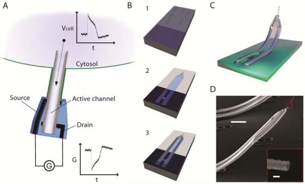
Here we demonstrate a conceptually new and practically simple field-effect transistor based probe that consists of a single semiconductor nanotube. The underlying principle of the active nanotube transistor, ANTT, intracellular probe (Figure 1A) involves the fabrication of S/D contacts to one end of a silicon or other semiconductor nanotube and electrical isolation of these S/D contacts from surrounding medium such that the solution filling the interior of the nanotube can gate the transistor and the variation of interior electrochemical potential is then recorded as a change in device conductance. Hence, if the free end of an ANTT probe is inserted into the interior of an electrogenic cell, the time-dependent changes associated with an action potential spike will give rise to time-varying conductance signal that maps the intracellular action potential. However, if a similarly configured solid silicon (or other semiconductor) nanowire is inserted into the cell, no signal would be observed since it would not be possible to ‘gate’ the transistor. We note that for p-type silicon nanotubes as used in our proof-of-concept studies, a positive change of intracellular potential yields a negative change in device conductance (Figure 1A), although the conductance can be quantitatively converted to potential using water-gate calibration measurements.1,7-9
Figure 1. Principle and fabrication of the ANTT probe.
(A) Schematic view of an ANTT probe inserted into a cell and recording an intracellular action potential (Vcell vs. time, t) as a conductance (G) change in the active FET region between S/D contacts. Sensitivity to voltage changes from the external extracellular environment is effectively eliminated by SU-8 passivation of the nanotube region around the S/D contacts. The nanotube is shown as a half-cylinder for clarity. (B) Overview of the steps used for ANTT probe fabrication:14 (1) Transfer of Ge/Si core/shell nanowires (Ge/Si NWs) to a SU-8 layer that was deposited and prebaked on a sacrificial layer (colored silver). (2) Registration of positions of Ge/Si NWs and definition of the bottom SU-8 layer. (3) Definition of S/D metal contacts followed by the top SU-8 passivation layer. Final etching of the sacrificial layer and Ge NW core yields the Si ANTT probe. (C) Schematic of the completed ANTT probe following release from the substrate. (D) Scanning electron microscopy (SEM) image of an ANTT probe. Scale bar, 10 μm. Inset, zoom of the probe tip from the dashed red box. Scale bar, 100 nm.
The fabrication of ANTT probes was carried out in several steps briefly illustrated in Figure 1B.14 First, Ge/Si core/shell NWs were synthesized by nanocluster catalyzed vapor-liquid-solid (VLS) growth of Ge NWs followed by p-type Si shell deposition as described previously.15-18 The Ge/Si NWs were dispersed from isopropyl alcohol or contact printed19-22 onto a prebaked SU-8 layer, which was initially deposited on a sacrificial nickel relief layer. After defining the lower SU-8 passivation/isolation layer by electron beam lithography (EBL), S/D metal contacts (Cr/Pd/Cr, 1.5/75/50 nm) followed by an upper SU-8 passivation/isolation layer were patterned by EBL. Etching the nickel sacrificial layer and Ge core of the Ge/Si NW yielded the p-type Si ANTT probe (Figure 1C). Scanning electron microscopy (SEM) images of ANTT probes (Figure 1D) confirm the basic fabrication strategy and show clearly the nanotube structure. Comparison of SEM images of ANTT device before and after the Ge core etching (Figure S1) show clearly the open tip and a ‘bright-to-dark’ change in image contrast along the length of the structure that is indicative of an open nanotube from the tip through to the S/D metal contacts. The “bend-up” angles, typically 40-60° and height, usually 15-30 μm in our design, are controlled by changing the length of the stressed bimetallic S/D arms as described previously.7
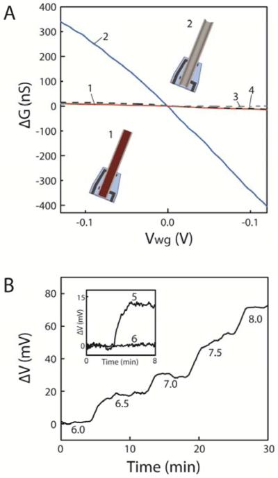
We have investigated the electrical properties of the probe structures fabricated in this manner in aqueous solution before and after etching the Ge NW cores. Prior to Ge-etching, conductance (G) versus water-gate potential (Vwg) data show only a small change with a sensitivity of ~0.10 μS/V (Figure 2A). Notably, after etching the Ge core to form the ANTT device the water-gate data exhibits a 30× sensitivity increase to 3.0 μS/V.23 These results are consistent with the increased gate coupling afforded by solution access to the Si-nanotube interior. To rule out the possibility that the Ge-etching process degrades the SU-8 passivation, we carried out control experiments on a Si/Si intrinsic-core/p-shell NW structure, where the shell is similar to the Ge/Si core/shell NWs used to make ANTT devices. Significantly, the Si/Si control device with SU-8 passivated S/D contacts showed similar sensitivity to the Ge/Si device and little or no sensitivity change following the same etching conditions used to remove Ge and yield the ANTT device. Taken together these results show that (1) the top/bottom SU-8 passivation effectively isolates the FET channel from external solution potential changes, and (2) the ANTT structure has good sensitivity to potential changes coupled through solution in the nanotube interior.
Figure 2. Potential and chemical sensitivities of ANTT devices.
(A) Change of conductance, ΔG, versus water-gate potential, Vwg, prior to (1) and after (2) H2O2 etching of the Ge NW core.14 Plots (3) and (4) correspond to ΔG versus Vwg for a Si/Si intrinsic-core/p-shell NW device before and after, respectively, etching using the same conditions as for the Ge/Si NW structure. All measurements were made in 1× phosphate-buffered saline (1×PBS) with a Ag/AgCl reference gate electrode. Insets, schematics of an ANTT device prior to (1) and after (2) H2O2 etching of the Ge NW core (colored deep red). (B) Change in potential, ΔV, in response to step changes in solution pH. The potential values were calculated from the measured ANTT device conductance using the measured water-gate sensitivity of 2.0 μS/V. Inset, ΔV as the pH is increased stepwise from 7.0 to 8.0 for an ANTT device (5) and the same device after closing the tip with SU-8 resist to prevent solution access (6).
In addition, we have explored the capability of the ANTT device to detect chemical changes in pH sensing experiments. Measurements of the G as a function of stepwise increasing pH showed a systematic increase with the increasing negative charge on the SiO2 surface24 of the p-type nanotube interior. These data plotted as change in potential versus solution pH (Figure 2B) yield a device pH sensitivity of up to 37 mV/pH, a value that is consistent with previous results reported for Si NW devices.7 Measurements made before and after closing the nanotube device end with SU-8 (inset, Figure 2B) confirm that this change is indeed due to pH detection from the solution inside the nanotube as no variation in G was observed after blocking solution exchange. These results show the potential of the ANTT probe to detect chemical and biochemical changes as previously demonstrated by nanowire FET sensors,7,24 although we note that necessity for diffusion of analytes within the nanotube will reduce the temporal resolution compared to external surface binding.
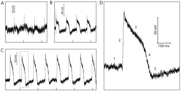
We explored the possibility of recording intracellular action potential with the ANTT probes using spontaneously firing chicken cardiomyocytes. In these experiments, ANTT probes relieved from the surface (e.g., Figure 1D) were modified with a phospholipid layer,7-9,25 cardiomyocytes were cultured on flexible sheets of polydimethlylsiloxane (PDMS) as described previously,25,26 and then the PDMS/cell sheet was moved to orient a single cell over an ANTT probe tip with an optical microscope. After contact with the cell, we initially observed regularly spaced spikes with a frequency of 1.8 Hz (Figure 3A) and correlated with cell beating. These peaks detected initially after contact had widths of ~0.7 ms and amplitudes up to 10 mV that are consistent with extracellular cardiomyocyte action potentials reported previously.1, 7, 26
Figure 3. Action potential recording with ANTT probes.
(A) Representative potential vs. time data recorded immediately following contact between the ANTT probe and a single cardiomyocyte. (B) Representative potential vs. time data recorded ca. 100 s following contact between the ANTT probe and a single cardiomyocyte and the trace in A. (C) Stable potential vs. time data recorded ca. 5 min following trace B. The tick marks in A-C correspond to 1 s. (D) Zoom of the single intracellular action potential peak in trace C highlighted with the dashed box. The five characteristic phases of the action potential peak, denoted by 1-5, are defined in text. In all the traces, the recorded device conductance was calibrated with the measured water-gate sensitivity to yield the plotted voltage signal.
Notably, over a period of ca. 100 seconds following contact between the ANTT probe tip and PDMS-supported cell the recorded periodic signals change substantially (Figure 3B) with an increase in amplitude and duration to 40-50 mV and ca. 200 ms respectively. Over a period of several minutes the peak amplitude continues to increase until stable periodic peaks are observed (Figure 3C) with amplitude and duration of ca. 80 mV and 200 ms, respectively. The peak duration and shape were similar to values reported for cardiomyocyte intracellular action potentials,27-29 and thus we can associate these data with intracellular action potential recording by the ANTT probe. Indeed, closer examination of a representative steady-state recorded peak (Figure 3D) shows five phases that can be associated with (1) resting state, (2) rapid depolarization, (3) plateau, (4) rapid repolarization, and (5) hyperpolarization, as discussed previously.7 We also note that preliminary experiments carried out with a smaller inner/outer diameter (15/50 nm) ANTT probe (Figure S2) showed similar intracellular action potential peaks with ca. 75 mV amplitude, consistent with the size-scaling predicted for the related BIT-FET.8
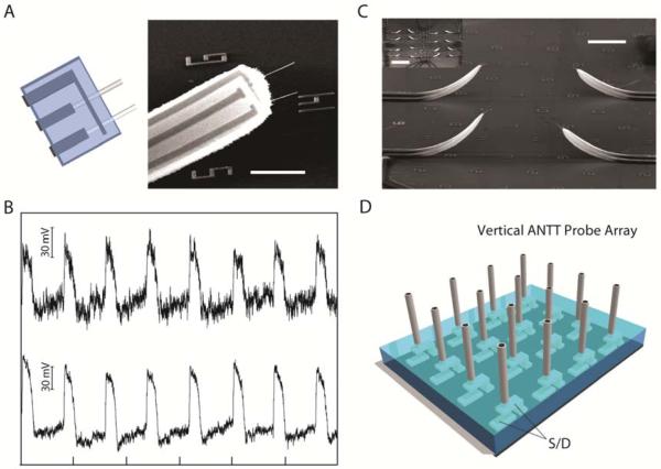
In addition, we have investigated two directions in multiplexed recording with the ANTT probe, including (1) multiple ANTT devices on a single probe and (2) arrays of ANTT probes. First, we fabricated probes with two ANTT devices as shown schematically in Figure 4A. Key steps in the fabrication involved contact-printing21 of the Ge/Si core/shell NWs to produce parallel NWs, and the use of a common source contact for both devices; the remainder of the fabrication process was similar to that described above.14 A representative SEM image (Figure 4A) shows clearly two ANTT devices on the single 3D probe with a nanotube tip-to-tip separation of ca. 7.6 μm. Notably, measurements made from two ANNT devices on a single probe following contact with one beating cardiomyocyte (Figure 4B) demonstrated regular intracellular action potential peaks from both devices. At steady-state the peaks recorded by both ANTT devices exhibited potential changes of about 80 mV consistent with intracellular action potentials and results reported recently for a two-element BIT-FET.8 Examination of the data recorded by both devices shows other important features. First, the noise in both channels is not correlated, and thus we can conclude that there is no significant electrical crosstalk between the dual-device/single-probe configuration even when recording from the same cell. Second, the S/N for one device (top trace, Figure 4B) is lower than that for the second device on the probe, which represents a limitation that will need to be improved in future for exploiting the potential of high spatial resolution recording using these multiplexed ANTT probes.
Figure 4. Multiplexed ANTT probes.
(A) Design and SEM image of a probe with two independent ANTT devices sharing a common source contact. Horizontal scale bar, 5 μm. (B) Intracellular recording from a single cardiomyocyte using a probe with two independent ANTT devices. The interval between tick marks corresponds to 1 s. (C) SEM image of part of an ANTT probe array fabricated from contact printed Ge/Si NWs. Scale bar, 2 μm. Inset, lower magnification SEM image of the 4 × 4 probe array. Scale bar, 100 μm. Probe interval is about 80 μm. (D) Schematic of chip-based vertical ANTT probe arrays fabricated using epitaxial Ge/Si NWs for enhanced integration.
Last, we have also extended our approach to fabricated arrays of ANTT probes. For example, a 4 × 4 array of single ANTT probes, with an average probe spacing of 80 μm, was fabricated from contact-printed Ge/Si NWs (Figure 4C). Denser ANTT probe arrays could be fabricated by varying the printing conditions.30 In addition, we are also exploring a strategy that involves epitaxial growth of ca. vertical Ge/Si NWs to produce high-density ANTT probe arrays (Figure 4D).31 In this approach, S/D contacts are defined vertically to the vertical semiconductor nanotubes in a manner similar to work on vertical nanowire FETs.32,33
In conclusion, we have demonstrated the design, synthesis, fabrication and testing of a new hollow needle-shaped nanoprobe based on an active silicon nanotube transistor termed the ANTT device. Measurements of conductance versus water-gate potential in aqueous solution have shown that the ANTT probe is selectively gated by potential change within the silicon nanotube, thus demonstrating the basic operating principle of the ANTT device. Studies interfacing ANTT probes with spontaneously beating cardiomyocytes demonstrated the recording of stable full-amplitude intracellular action potentials, and moreover, showed that full-amplitude action potentials could be recorded with inner tube diameters as small as 15 nm. In addition, the straightforward fabrication of ANTT devices was exploited to prepare multiple ANTTs at the end of single probes, which enabled multiplexed recording of full-amplitude intracellular action potentials from single cells, and multiplexed arrays of single ANTT device probes. These studies open up unique opportunities for multisite recordings from individual cells through cellular networks, including the potential for intracellular chemical sensing through modification of the inner tube surface.34
Supplementary Material
Acknowledgements
The authors acknowledge J. Huang and D. Bell for helpful discussions. R. G. acknowledges a Japan Student Services Organization Graduate Research Fellowship. S. S. acknowledges financial support by the German Research Foundation (STR1119/2). C.M.L. acknowledges support from a NIH Director‘s Pioneer Award (1DP1OD003900).
References
- 1.Timko BP, Cohen-Karni T, Qing Q, Tian B, Lieber CM. IEEE Trans. Nanotechnol. 2010;9:269–280. doi: 10.1109/TNANO.2009.2031807. [DOI] [PMC free article] [PubMed] [Google Scholar]
- 2.Lieber CM. MRS Bull. 2011;36:1052–1063. doi: 10.1557/mrs.2011.269. [DOI] [PMC free article] [PubMed] [Google Scholar]
- 3.Sakmann B, Neher E. Annu. Rev. Physiol. 1984;46:455–472. doi: 10.1146/annurev.ph.46.030184.002323. [DOI] [PubMed] [Google Scholar]
- 4.Rutten WLC. Annu. Rev. Biomed. Engl. 2002;4:407–452. doi: 10.1146/annurev.bioeng.4.020702.153427. [DOI] [PubMed] [Google Scholar]
- 5.Purves RD. Microelectrode Methods for Intracellular Recording and Ionophoresis. Academic Press; New York: 1981. [Google Scholar]
- 6.Chorev E, Epsztein J, Houweling AR, Lee AK, Brecht M. Curr. Opin. Neurobiol. 2009;19:513–519. doi: 10.1016/j.conb.2009.08.005. [DOI] [PubMed] [Google Scholar]
- 7.Tian B, Cohen-Karni T, Qing Q, Duan X, Xie P, Lieber CM. Science. 2010;329:831–834. doi: 10.1126/science.1192033. [DOI] [PMC free article] [PubMed] [Google Scholar]
- 8.Duan X, Gao R, Xie P, Cohen-Karni T, Qing Q, Choe HS, Tian B, Jiang X, Lieber CM. Nat. Nanotechnol. 2012;7:174–179. doi: 10.1038/nnano.2011.223. [DOI] [PMC free article] [PubMed] [Google Scholar]
- 9.Jiang Z, Qing Q, Xie P, Gao R, Lieber CM. Nano Lett. 2012;7:1711–1716. doi: 10.1021/nl300256r. [DOI] [PMC free article] [PubMed] [Google Scholar]
- 10.Hai A, Shappir J, Spira ME. Nat. Methods. 2010;7:200–202. doi: 10.1038/nmeth.1420. [DOI] [PubMed] [Google Scholar]
- 11.Xie C, Lin Z, Hanson L, Cui Y, Cui B. Nat. Nanotechnol. 2012;7:185–190. doi: 10.1038/nnano.2012.8. [DOI] [PMC free article] [PubMed] [Google Scholar]
- 12.Robinson JT, Jorgolli M, Shalek AK, Yoon M-H, Gertner RS, Park H. Nat. Nanotechnol. 2012;7:180–184. doi: 10.1038/nnano.2011.249. [DOI] [PMC free article] [PubMed] [Google Scholar]
- 13.Cohen-Karni T, Casanova D, Cahoon JF, Qing Q, Bell DC, Lieber CM. Nano Lett. 2012 doi: 10.1021/nl3011337. Article ASAP. DOI: 10.1021/nl3011337. [DOI] [PMC free article] [PubMed] [Google Scholar]
- 14.ANTT probes were fabricated on the Si3N4 surface of silicon substrates (100 nm thermal SiO2, 200 nm Si3N4, n-type, 0.005 V·cm, Nova Electronic Materials). A Ni sacrificial layer (80 nm) was first defined by electron beam lithography (EBL) and thermal evaporation (TE). The substrate was then coated with SU-8 resist (2000.5, MicroChem Corp.), on which the as-synthesized Ge/Si core/shell nanowires were deposited by either of two methods: (1) nanowires suspended in isopropyl alcohol were deposited from solution; or (2) nanowires were directly contact-printed as described previously.21 After definition of the bottom SU-8 support layer by EBL, source/drain (S/D) metal contacts were defined by EBL and metalized by thermal evaporation of Cr/Pd/Cr (1.5/75/50 nm). Typically, the S/D contact separation was 0.5-1 μm and the free end of the nanowire extended 3-4 μm from the source contact. The top SU-8 layer was subsequently defined by EBL for passivation. Etching of the Ni sacrificial layer (1.5 h) in nickel etchant (TFB, Transene Company, Inc.) and the Ge core of the core/shell nanowire (65°C, 30-60 min) in hydrogen peroxide (H2O2, 30%, Sigma) yielded the ANTT probes.
- 15.Lauhon LJ, Gudiksen MS, Wang D, Lieber CM. Nature. 2002;420:57–61. doi: 10.1038/nature01141. [DOI] [PubMed] [Google Scholar]
- 16.Timko BP. Ph.D. Thesis. Harvard University; Cambridge, MA: 2009. Semiconductor nanowire devices: Novel morphologies and applications to electrogenic biological systems. [Google Scholar]
- 17.Ben-Ishai M, Patolsky F. J. Am. Chem. Soc. 2009;131:3679–3689. doi: 10.1021/ja808483t. [DOI] [PubMed] [Google Scholar]
- 18.Ge/Si core/shell nanowires were synthesized by gold-nanocluster catalyzed vapor-liquid-solid (VLS) process as described previously.15-17 Briefly, 50 or 15 nm diameter gold nanoparticles (Ted Pella) were dispersed on Si/SiO2 substrates (Nova Electronic Materials). The Ge core growth was carried out using GeH4 (20-30 sccm, 10% in H2) and H2 (200 sccm) for 30 min at a total pressure of 300-400 Torr and temperature of 270-310 °C. The p-type Si shell (ca. 25 nm in thickness) was subsequently grown on the 50 nm Ge core by uncatalyzed decomposition of SiH4 (1 sccm) and B2H6 (10 sccm, 100 ppm in H2) at a total pressure of 20 Torr and temperature of 475°C for 30 min. We note that p-type Si shell (15-20 nm) growth on the 15 nm Ge core was carried out at a reduced deposition rate: 3 sccm SiH4, 15 sccm B2H6 (100 ppm in H2) and 50 sccm H2 at a total pressure of 9 Torr and temperature of 450°C for 40 min. A final annealing step at 600 °C for 1.5 h under vacuum (2.8 × 10⁻³ Torr) gave crystalline Ge/Si core/shell nanowires.
- 19.Patolsky F, Zheng G, Lieber CM. Nat. Prot. 2006;4:1711–1724. doi: 10.1038/nprot.2006.227. [DOI] [PubMed] [Google Scholar]
- 20.Whang D, Jin S, Lieber CM. Nano Lett. 2003;3:951–954. [Google Scholar]
- 21.Javey A, Nam S, Friedman RS, Yan H, Lieber CM. Nano Lett. 2007;7:773–777. doi: 10.1021/nl063056l. [DOI] [PubMed] [Google Scholar]
- 22.Yu G, Cao A, Lieber CM. Nat. Nanotechnol. 2007;2:372–377. doi: 10.1038/nnano.2007.150. [DOI] [PubMed] [Google Scholar]
- 23.ANTT device sensitivity (S/V) was defined as S/D conductance change in response to gate voltage (Vwg) applied by Ag/AgCl reference electrode. Vwg was typically swept at a rate of 80 mV/s from −0.4 V to +0.4 V. The S/D current, driven by 100 mV source voltage, was amplified by a current preamplifier (1211, DL Instruments) at sensitivity of 10−6 or 10−7 A/V, filtered (0-3 kHz, CyberAmp 380, Molecular Devices, Inc.) and digitized at 50-250 kHz sampling rate (Axon Digidata 1440A Data Acquisition System, Molecular Devices, Inc.).
- 24.Cui Y, Wei Q, Park H, Lieber CM. Science. 2001;293:1289–1292. doi: 10.1126/science.1062711. [DOI] [PubMed] [Google Scholar]
- 25.Embryonic chicken cardiomyocytes on PDMS were prepared using published protocols.26 Before intracellular recording, probe chips were incubated with lipid vesicles of 1,2-dimyristoyl-sn-glycero-3-phosphocholine (DMPC, Avanti Polar Lipids Inc.) containing 1% 1-myristoyl-2-{12-[(7-nitro-2-1,3-benzoxadiazol-4-yl) amino] dodecanoyl}-sn-glycero-3-phosphocholine (NBD-lipid, Avanti Polar Lipids Inc.) as fluorescence reporter using a procedure described earlier.7 The recordings were carried out in 1× Tyrode solution (pH 7.3) at 37°C using a 100 mV DC source voltage for ANTT devices. The S/D current was converted to voltage with a current preamplifier, low-pass filtered and digitized as described previously.23 A pulled glass micropipette was used for manipulation of the cardiomyocytes/PDMS sheet.26
- 26.Cohen-Karni T, Timko BP, Weiss LE, Lieber CM. Proc. Natl. Acad. Sci. U. S. A. 2009;106:7309–7313. doi: 10.1073/pnas.0902752106. [DOI] [PMC free article] [PubMed] [Google Scholar]
- 27.Zipes DP, Jalife J. Cardiac electrophysiology: from cell to bedside. 5th ed Saunders; Philadelphia: 2009. [Google Scholar]
- 28.Bers DM. Nature. 2002;415:198. doi: 10.1038/415198a. [DOI] [PubMed] [Google Scholar]
- 29.Connolly P, Clark P, Curtis AS, Dow JA, Wilkinson CD. Biosensors & Bioelectronics. 1990;5:223–234. doi: 10.1016/0956-5663(90)80011-2. [DOI] [PubMed] [Google Scholar]
- 30.Yan H, Choe HS, Nam SW, Hu Y, Das S, Klemic JF, Ellenbogen JC, Lieber CM. Nature. 2011;470:240–244. doi: 10.1038/nature09749. [DOI] [PubMed] [Google Scholar]
- 31.Gao R, Strehle S, Lieber CM. unpublished results. [Google Scholar]
- 32.Goldberger J, Hochbaum AI, Fan R, Yang P. Nano Lett. 2006;6:973–977. [Google Scholar]
- 33.Bryllert T, Wemersson L, Froberg LE, Samuelson L. IEEE Electron Device Lett. 2006;27:323–325. [Google Scholar]
- 34.Ben-Ishai M, Patolsky F. J. Am. Chem. Soc. 2011;133:1545–1552. doi: 10.1021/ja109197u. [DOI] [PubMed] [Google Scholar]
Associated Data
This section collects any data citations, data availability statements, or supplementary materials included in this article.


