Abstract
PbSe is a surprisingly good thermoelectric material due, in part, to its low thermal conductivity that had been overestimated in earlier measurements. The thermoelectric figure of merit, zT, can exceed 1 at high temperatures in both p-type and n-type PbSe, similar to that found in PbTe. While the p-type lead chalcogenides (PbSe and PbTe) benefit from the high valley degeneracy (12 or more at high temperature) of the valence band, the n-type versions are limited to a valley degeneracy of 4 in the conduction band. Yet the n-type lead chalcogenides achieve a zT nearly as high as the p-type lead chalcogenides. This effect can be attributed to the weaker electron–phonon coupling (lower deformation potential coefficient) in the conduction band as compared with that in the valence band, which leads to higher mobility of electrons compared to that of holes. This study of PbSe illustrates the importance of the deformation potential coefficient of the charge-carrying band as one of several key parameters to consider for band structure engineering and the search for high performance thermoelectric materials.
Keywords: energy, semiconductor, quality factor
Waste heat recovery using thermoelectric power generation is attracting considerable interest from the automobile industry (1) as well as from many other areas (2). Large-scale production of bulk materials with high figure of merit, zT, defined as zT = S2σT/(κe + κL) (S is the Seebeck coefficient, σ is the electric conductivity, and κe and κL are the electronic and lattice thermal conductivity, respectively), is the key to widespread adaption of thermoelectric technology. The search for good thermoelectric materials has focused on investigating semiconductors that have suitable band structures and low thermal conductivities (3, 4). As one of the first investigated material systems (5), PbTe and its alloys have been extensively studied and remain some of the best (6, 7) thermoelectric materials for applications from 500 to 900 K. Considerable effort has been made to achieve a higher zT in these alloys by reducing the lattice thermal conductivity, κL, by incorporation of nanometer scale inclusions (8–11). Other strategies approach the challenge of increasing zT from different angles, such as band structure distortion by Tl doping (12), and more recently, increasing band degeneracy by converging two different valence bands in p-type PbTe (13).
It can be shown that the material parameter called the thermoelectric quality factor, B,
 |
[1] |
determines the optimized figure of merit (14–16) (NV is the band degeneracy,  is the density of states effective mass of a single band, μ0 is the mobility at nondegenerate limit, and κL is the lattice thermal conductivity). This expression is derived for semiconductors with single band transport behavior where the carrier concentration can be optimized to achieve maximum zT. For good thermoelectric semiconductors the dominant scattering mechanism at high temperatures, where zT peaks, is typically due to acoustic phonons. The deformation potential theory of Bardeen and Shockley (17) enables the nondegenerate mobility, μ0, in B to be replaced with parameters more descriptive of the band structure, namely the effective mass and deformation potential coefficient, Ξ, of the conducting band. This gives the resulting expression when multivalley conduction is considered (18):
 |
[2] |
where  is the inertial effective mass and Cl is a combination of elastic constants. The deformation potential coefficient describes the change in energy of the electronic band with elastic deformation and thus describes the interaction, or coupling, between electrons and phonons.
Including this relationship in the expression for B reveals
 |
[3] |
Because κL is generally independent of electronic band structure* (19), this relation for B suggests that Ξ is an important factor determining the maximum performance of a thermoelectric material.
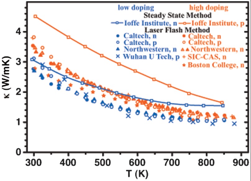
The high thermoelectric performance of p-type PbSe, a lower cost analog of PbTe, has been a relatively recent discovery (20–22). Originally, PbSe was thought to be significantly inferior to PbTe because of higher thermal conductivity and lower band gap (22). This turns out not to be the case at high temperatures where zT is greatest. The lattice thermal conductivity of PbSe is nearly as low as PbTe because of the larger (21) Grüneisen parameter of PbSe relative to PbTe while the band gap of PbSe increases rapidly with temperature, actually exceeding that of PbTe above 500 K (23, 24). Like with PbTe, the zT for PbSe can be greater than 1 with dense samples, optimal doping, and utilizing the thermal diffusivity technique for thermal conductivity measurements. In this study, we have measured a peak zT for Br-doped PbSe to be 1.1 ± 0.1 at 850 K in five different samples, using different measurement techniques in different institutions on the same sample (see Fig. 1 and SI Material for comparison of each property and zT for Br-doped samples measured at Caltech, Shanghai Institute of Ceramics–Chinese Academy of Sciences, and Jet Propulsion Laboratory).
Fig. 1.
A comparison of thermal conductivity of PbSe measured using the steady-state method and the laser flash method. Data are shown in two different groups (details shown in SI Material) according to the carrier density. All the laser flash measurements show similar behavior despite the differences in composition, while the steady-state method gives higher thermal conductivities.
Early measurement on optimally doped PbTe and PbSe had overestimated the thermal conductivity, which has led to an underestimate (7) of zT. This overestimation of thermal conductivity can be traced to the unavailability of data (25) or the technique for high temperature thermal conductivity. Today the most used technique for high temperature thermal conductivity is the flash diffusivity method as opposed to the steady-state method because of inaccuracies resulting from radiation losses during measurement (26). Our thermal conductivity measurements on PbSe are consistent with those of other laboratories using the same diffusivity technique (some reported subsequent to the original submission of this manuscript). The thermal conductivity measured by the steady-state method (22) is significantly higher than that measured by five independent groups using the diffusivity technique (Fig. 1).
Additionally, high zT in p-type PbSe is attributed to the high band degeneracy (NV≥12) at high temperatures (13, 21). Conversely, the conduction band for PbSe has a much lower band degeneracy of 4. With these attributes in mind, n-type PbSe should not be expected to have high zT; nevertheless, with optimized carrier density, zT is found to be as high as approximately 1.2 at 850 K, as shown below. The explanation for the surprisingly large zT is a smaller deformation potential coefficient of the conduction band compared to the valence band, as evidenced by high carrier mobility resulting from weak scattering.
N-type PbSe is formed by substitution of Se2- with a halogen, such as Br-, with one conducting electron produced for each substituted atom. A slight amount of excess Pb is commonly used (25, 27) to minimize compensating metal vacancies that lead to p-type conduction as well as to improve the mechanical strength. Br is chosen in this study because it is closest in atomic size and electronic structure to Se and thus is expected to have minimal effect on the carrier mobility.
The Hall carrier density (nH = 1/eRH,RH is the measured Hall coefficient) can be tuned from 7 × 10¹⁸ to 5 × 1019 cm-3 by controlling the dopant concentration. The samples are identified with their Hall carrier density at 300 K for the following discussion while their nominal compositions are given in SI Material.
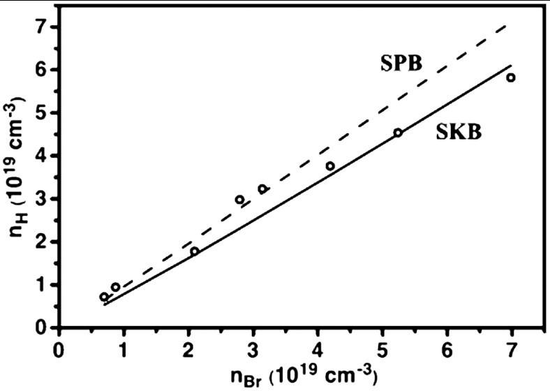
The measured values of nH are in good agreement with expected value based on Br content (Fig. 2). Exactly one electron in the conduction band per Br atom is expected for PbSe1-xBrx based on the simple valence principle, which provides a good model for heavily doped thermoelectric semiconductors (28). Earlier results on Cl doped PbSe appear to follow this valence principle (22), while more recent results on Cl doped PbSe show far fewer carriers than expected. The fewer than expected carriers may indicate the presence of other bulk or surface defects that lead to the reduced mobility of these samples (29).
Fig. 2.
The measured Hall carrier density as a function of Br concentration. The observed value matches reasonably well with expected value using the single Kane band model (SKB) or single parabolic band model (SPB).
PbSe is a small band gap semiconductor in which the direct band gap forms between bands with small band mass (30). The band extrema is located at the L point of the Brillouin zone and has four equivalent ellipsoid pockets (24) (NV = 4) that dominate the transport properties for n-type PbSe. As with all lead chalcogenides, the conduction band (and the light valence band) have been shown to be nonparabolic (7, 23, 31–33), with transport properties that can be well characterized by the single Kane band (SKB) model (24). It is confirmed here that the SKB model quantitatively explains the observed electronic transport properties throughout the temperature and doping range discussed in this paper (SI Material).
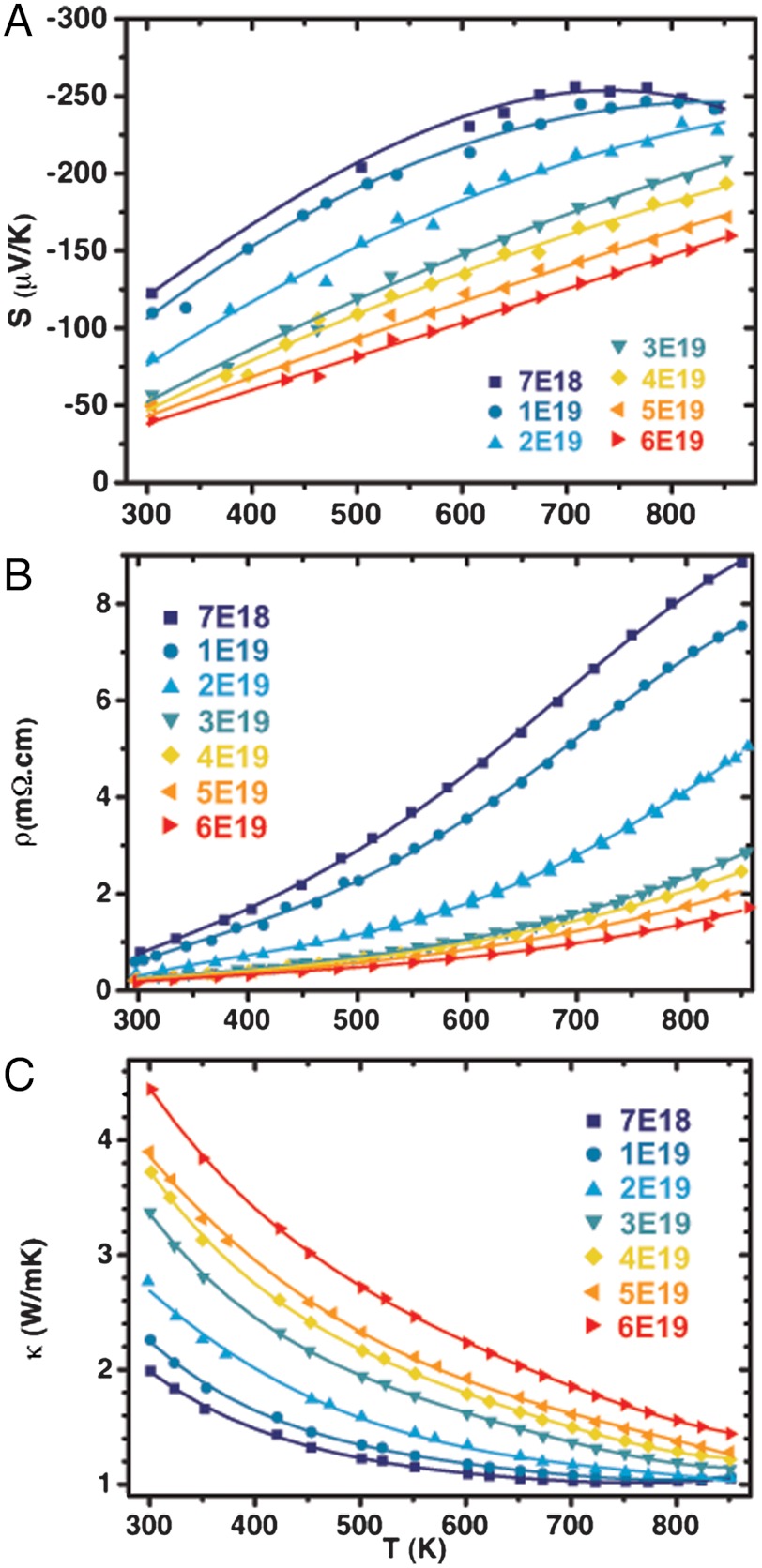
Both the Seebeck coefficient and resistivity increase with increasing temperature for the majority of the samples in this study, as shown in Fig. 3 A and B, respectively. These trends are consistent with degenerate semiconducting behavior.
Fig. 3.
Thermoelectric transport properties of Br-doped PbSe as function of temperature. (A) Seebeck coefficient, (B) resistivity, and (C) thermal conductivity.
The total thermal conductivity (Fig. 3C) decreases with temperature, reducing to 1.0–1.4 W/mK at 850 K, depending on the doping level. The lattice thermal conductivity, κL, is calculated by subtracting the electronic contribution (κe = LT/ρ) from the measured total thermal conductivity, where L is calculated using the SKB model. The κL for several optimally doped samples, as well as the averaged value (dashed line), are shown in SI Material and indicate a κL of approximately 0.8 W/mK at 850 K, which is consistent with the previously reported (21) value for κL of p-type PbSe (approximately 0.6 W/mK at 850 K)
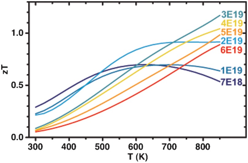
The zT values as a function of temperature are shown in Fig. 4. The optimal doping level is found to be around 3 × 1019 cm-3, achieving zT as high as 1.2 at 850 K. The zT value of 1.0 ∼ 1.2 was obtained in multiple samples with room temperature nH between 2.9 and 3.4 × 1019 cm-3 and whose transport properties were measured both perpendicular and parallel to the hot press direction (SI Material).
Fig. 4.
zT as function of temperature for Br-doped PbSe.
It may be surprising that zT > 1 can be achieved in properly doped n-type PbSe where a single band with a relatively small NV = 4 is responsible for the electronic transport properties. In comparison, the light valence band of p-type PbSe with same  and NV as the conduction band has a much lower zT (SI Material). Properly doped p-type PbSe achieves high zT at high temperatures due to the influence of the heavy valence band, which produces an extraordinarily large number of valleys (NV≥12) (13, 21). Thus, high zT in n-type PbTe suggests an advantage in the character of the conduction band that compensates for the relatively low number of degenerate valleys. The accuracy of the SKB model in characterizing carrier transport in the light bands at the L point, in combination with the fact that the effective mass and elastic properties (i.e., Cl) of the n-type and p-type PbSe are found to be the same, allow for the compensating effect in the n-type material to be traced to the deformation potential coefficient (Ξ), as discussed below.
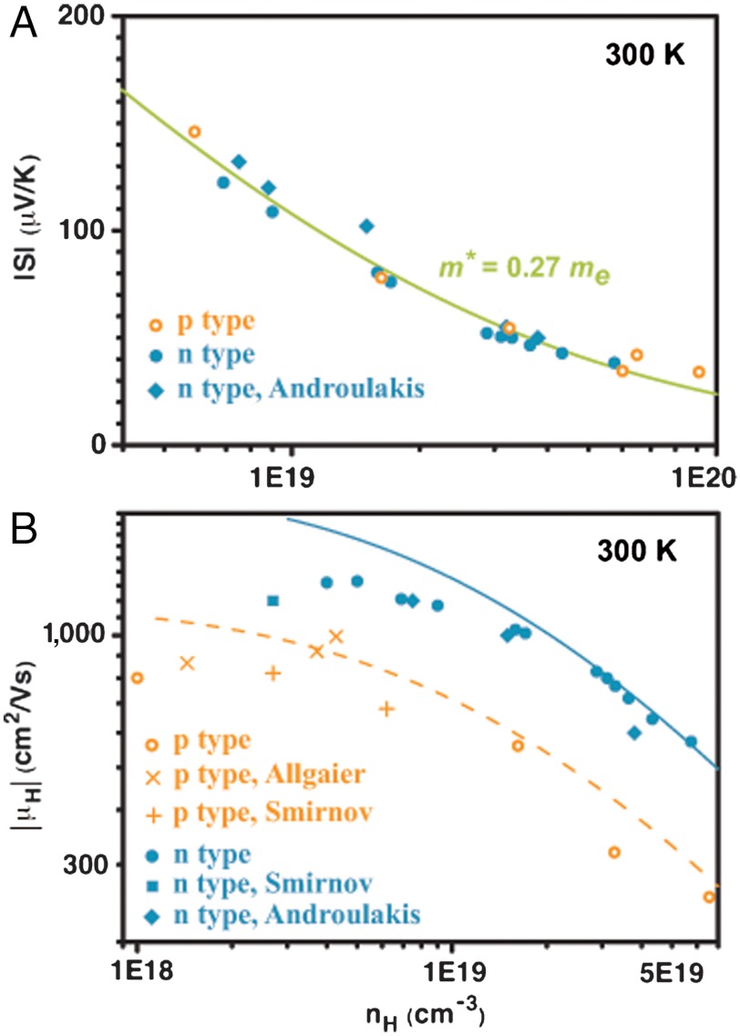
Fig. 5A shows the Seebeck coefficient versus Hall carrier density at 300 K for both n- and p-type samples. The agreement of the calculated curve for both materials indicates that the density of states effective mass,  , is the same (m∗ = 0.27 me) for both the conduction band and the light valence band. In addition, the speed of sound was measured and found to be comparable (vl ≈ 3,200 m/s, vt ≈ 1,700 m/s) for both p- and n-type PbSe. By these consistencies, it is implied that the parameter Cl, determined by the elastic moduli, remains unchanged for both n- and p-type samples.
Fig. 5.
Thermoelectric properties of n-type and p-type PbSe. (A) Seebeck coefficient and (B) Hall mobility as function of Hall carrier density at 300 K. All curves are calculated from SKB model.
Fig. 5B shows the Hall mobility (μH) of n- and p-type samples at 300 K as well as data reported by Smirnov (34), Allgaier (35), and Androulakis (29). The p-type samples are selected such that the carrier density is relatively low and thus the influence from the heavy band at this temperature is negligible. It is clearly seen that the mobility of the n-type material is much higher than that of the p-type material over the entire carrier density range [there are previous studies supporting this result (34, 36, 37), while there are also other reports suggesting that the mobility is similar between n- and p-type PbSe at room temperature (35, 38)]. Furthermore, the SKB model provides excellent prediction of μH vs. nH at 300 K for both n- and p-type materials at high doping levels where acoustic phonon scattering is the dominant mechanism. The curves to model the mobility data for each material can be obtained by using different deformation potential coefficient values (in absolute value), while all other model parameters are the same: for n-type samples, the parameter is Ξ = 25 eV, while for p-type samples, Ξ = 35 eV. The deformation potential coefficient represents the degree to which the charge carriers interact with phonons in the material. Therefore, the lower Ξ value in the n-type material reveals that the carriers are less scattered by acoustic phonons in the conduction band compared with those in the valence band.
The result that Ξ is approximately 10 eV smaller in the conduction band than in the light valence band is supported by both calculations and experimental characterization of the optical deformation potential, Diso, of both PbSe and PbTe. By definition, Diso is calculated by subtracting the isotropic deformation potential, which is related to Ξ (39), of the valence band from that of the conduction band, where both values are negative for lead chalcogenides. Zasavitskii (40) determined Diso = 14 eV at 295 K for PbSe in quantum well structures from photoluminescence and X-ray diffraction data. Ferreira (41) calculated Diso to be approximately 10 eV for PbTe using the Augmented-Plane-Wave method. These values are in reasonable agreement with the Diso estimated from the elastic moduli (42) and the experimental change in band gap due to pressure (24) [approximately 13 eV for PbSe, approximately 10 eV for PbTe (41)] as well as thermal expansion and temperature dependence of the energy gap (24) [approximately 21 eV for PbSe, approximately 15 eV for PbTe (41)] using the relationship given by Ferreira (41).
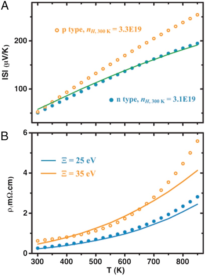
The temperature dependent Seebeck coefficient and resistivity of both n- and p-type PbSe are compared with the SKB model results and shown in Fig. 6 A and B, respectively. The two samples shown have approximately the same carrier density (nH,300 K ∼ 3 × 1019 cm-3). Using parameters determined in this work, the SKB model successfully predicts both the Seebeck coefficient and resistivity for n-type PbSe up to 850 K. The SKB model is poor for p-type PbSe, especially at high temperatures, due to the transport behavior resulting from two contributing bands. Most importantly, it is clearly seen that at lower temperatures, where the light valence band dominates the transport properties of p-type PbSe (Fig. 6B), n-type PbSe shows much weaker carrier scattering (due to smaller Ξ) than p-type material, resulting in a lower resistivity, and ultimately high zT.
Fig. 6.
Thermoelectric properties (A) Seebeck coefficient and (B) resistivity for n-type and p-type PbSe having similar carrier density. All curves are calculated from SKB model (note that the calculated Seebeck coefficient for the n- and p-type is the same and does not depend on Ξ) showing that while the n-type data fits the SKB model at all temperatures well, the p-type shows deviations at higher temperature due to two-band behavior.
In the single Kane band model, the same quality factor B defined by Eq. 3 is found to characterize the suitability of the band structure through the expression of zT:
 |
[4] |
The ξ and  (see SI Material for definition) dependent terms can be optimized via carrier density tuning. Subsequently, the maximum zT one could achieve for the optimized carrier density is determined by the quality factor B. In p-type PbSe the effective band degeneracy, NV, is large because of the convergence of two different valence bands, which leads to a large B and high zT. In n-type PbSe, although NV is smaller, high zT is achieved as a result of comparable quality factor, B, which stems from a smaller Ξ.
Ξ for a few semiconductor systems are found in the range of 5 to 35 eV (SI Material). Given a certain material system, the maximum zT achieved by carrier density tuning would be further increased if the deformation potential of bands participating in carrier transport could be engineered. The latter has been shown possible at least in low dimensional systems: Murphy-Armando and Fahy (43) found that the deformation potential of Γ band of n-type Ge film is decreased with strain. Also, in Si thin films embedded between hard layers of diamond (44), the mobility is found increased due to suppressed deformation potential electron–phonon scattering.
Since the original submission of this manuscript there have been reports on transport properties in n-type PbSe doped with group III elements (45) and chlorine (29), as well as nanostructured (46) PbSe1-xSx. Our discussion here involves complementary phenomena that should have some applicability to these results.
In summary, n-type PbSe doped with Br achieves zT values exceeding 1 at 850 K, similar to that found in p-type PbSe, making PbSe a competitive and less expensive alternative to PbTe for both types. In p-type PbSe, high zT is achieved due to the convergence of the light and heavy valence bands, acting to effectively increase band degeneracy. In n-type PbSe, with relatively low band degeneracy, high zT is achieved as a result of a low deformation potential coefficient characterizing weak scattering of the charge carriers in the conduction band. This study demonstrates the importance of the deformation potential coefficient in selecting and engineering optimum band structures for thermoelectrics.
This paper highlights a discrepancy between thermal conductivity data obtained via commonly accepted laser flash method compared to the less commonly used steady-state method such as that performed by the Ioffe Institute. Because the Ioffe technique includes a radiation shield and finds no significant error resulting from radiation losses during measurement, there is no reason to believe the Ioffe data are less reliable. Thus, it will be important to the field to organize a comprehensive comparison between the two methods.
Materials and Methods
Polycrystalline samples of Pb1.002Se1-xBrx with x changing from 0.04% to 0.4% were prepared using a melt alloying and hot pressing technique. Pure elements and PbBr2 (Pb, 99.999%; Se, 99.999%; PbBr2 99.999%, ultra dry) were weighed out according to each composition and loaded into quartz ampoules, which were then evacuated and sealed. The sealed ampoules were slowly heated up to 1,400 K and kept for 12 h followed by a water quench. The ingots obtained were further annealed at 950 K for 72 h before being crushed and ground into fine powders. The powders were then hot pressed (47) at 873 K under 1 atm argon with 40 MPa pressure for 20 min, followed by another 60 min of annealing at 873 K without pressure. A typical disk shaped sample obtained is 12 mm in diameter, approximately 1 mm in thickness, with density no less than 98% of theoretical density (8.27 g/cm3). Samples were single phase according to XRD results on the hot pressed disks. Analysis by a scanning Seebeck probe showed homogeneous Seebeck coefficient with standard deviation of 3.7 μV/K (approximately 5% in Seebeck coefficient).
The in-plane resistivities and Hall coefficients (RH) were measured using the Van der Pauw method in a magnetic field up to ± 2 T. The free surface of the sample was coated with insulating BN, which successfully prevented sample degradation at high temperature in vacuum. The Seebeck coefficients were obtained along the cross-plane direction by measuring the thermoelectric voltages as well as temperatures (48). The cross-plane thermal conductivities were obtained from κ = dDTCp, with the thermal diffusivity DT measured by the laser flash method (Netzsch LFA 457), where d is the geometric density. The heat capacity Cp was determined using the equation Cp/kB atom-1 = 3.07 + 4.7 × 10⁻⁴ (T/K-300) based on experimental results (49) and is believed to be accurate for lead chalcogenides (7, 13, 21, 50, 51).
All the measurements were carried out under vacuum, and data were collected during both heating and cooling with both datasets shown. As seen in the figures, no hysteresis was observed. In addition, the temperature dependent resistivities were retested after the other high temperature measurements were done, and no appreciable change was found. The uncertainty of each measurement is estimated to be approximately 5%, which combined leads to approximately 20% uncertainty for zT. More details about the measurement uncertainty are discussed in the supplementary material.
Supplementary Material
Acknowledgments.
The authors thank Xun Shi and Lidong Chen at Shanghai Institute of Ceramics–Chinese Academy of Science and Alexandra Zevalkink at Jet Propulsion Laboratory for confirming measurements, and Defense Advanced Research Planning Agency’s Nano-Structured Materials for Power program and National Aeronautics and Space Administration–Jet Propulsion Laboratory for financial support.
Footnotes
The authors declare no conflict of interest.
This article is a PNAS Direct Submission. A.S. is a guest editor invited by the Editorial Board.
This article contains supporting information online at www.pnas.org/lookup/suppl/doi:10.1073/pnas.1111419109/-/DCSupplemental.
*When κL is dominated by Umklapp scattering, typically the most important phonon scattering process for thermoelectrics above room temperature, it can be related to other physical properties as  . In the case for glass-like phonon thermal conductivity, κL is related to these properties as
  , where C is a combination of elastic moduli, d is the density,V is the volume per atom and γ the Grüneisen parameter (see ref. 19). The parameters characterizing the electronic band structure, such as deformation potential, are not seen in these relations
References
- 1.Bell LE. Cooling, heating, generating power, and recovering waste heat with thermoelectric systems. Science. 2008;321:1457–1461. doi: 10.1126/science.1158899. [DOI] [PubMed] [Google Scholar]
- 2.Kajikawa T. In: CRC Thermoelectric Handbook. Rowe DM, editor. Boca Raton, FL: CRC Press; 2006. pp. 50-1–50-26. [Google Scholar]
- 3.Snyder GJ, Toberer ES. Complex thermoelectric materials. Nat Mater. 2008;7:105–114. doi: 10.1038/nmat2090. [DOI] [PubMed] [Google Scholar]
- 4.Minnich AJ, Dresselhaus MS, Ren ZF, Chen G. Bulk nanostructured thermoelectric materials: Current research and future prospects. Energy Environ Sci. 2009;2:466–479. [Google Scholar]
- 5.Wood C. Materials for thermoelectric energy-conversion. Rep Prog Phys. 1988;51:459–539. [Google Scholar]
- 6.Pei Y, LaLonde A, Iwanaga S, Snyder GJ. High thermoelectric figure of merit in heavy hole dominated PbTe. Energy Environ Sci. 2011;4:2085–2089. [Google Scholar]
- 7.LaLonde AD, Pei Y, Snyder GJ. Reevaluation of PbTe1-xIx as high performance n-type thermoelectric material. Energy Environ Sci. 2011;4:2090–2096. [Google Scholar]
- 8.Pei Y, Lensch-Falk J, Toberer ES, Medlin DL, Snyder GJ. High thermoelectric performance in PbTe due to large nanoscale Ag2Te precipitates and La doping. Adv Funct Mater. 2011;21:241–249. [Google Scholar]
- 9.Pei Y, May AF, Snyder GJ. Self-tuning the carrier concentration of PbTe/Ag2Te composites with excess Ag for high thermoelectric performance. Adv Energy Mater. 2011;1:291–296. [Google Scholar]
- 10.He JQ, Girard SN, Kanatzidis MG, Dravid VP. Microstructure-lattice thermal conductivity correlation in nanostructured PbTe07S0.3 Thermoelectric Materials. Adv Funct Mater. 2010;20:764–772. [Google Scholar]
- 11.Poudeu PFR, et al. High thermoelectric figure of merit and nanostructuring in bulk P-Type Na1-XPbmSbyTem+2. Angew Chem Int Ed Engl. 2006;45:3835–3839. doi: 10.1002/anie.200600865. [DOI] [PubMed] [Google Scholar]
- 12.Heremans JP, et al. Enhancement of thermoelectric efficiency in PbTe by distortion of the electronic density of states. Science. 2008;321:554–557. doi: 10.1126/science.1159725. [DOI] [PubMed] [Google Scholar]
- 13.Pei Y, et al. Convergence of electronic bands for high performance bulk thermoelectrics. Nature. 2011;473:66–69. doi: 10.1038/nature09996. [DOI] [PubMed] [Google Scholar]
- 14.Goldsmid HJ. Thermoelectric Refrigeration. London: Temple Press Books LTD; 1964. [Google Scholar]
- 15.Mahan GD. Solid State Physics Vol 51: Solid State Physics—Advances in Research and Applications. New York: Academic; 1998. pp. 81–157. [Google Scholar]
- 16.Chasmar RP, Stratton R. The thermoelectric figure of merit and its relation to thermoelectric generators. J Electron Control. 1959;7:52–72. [Google Scholar]
- 17.Bardeen J, Shockley W. Deformation potentials and mobilities in non-polar crystals. Phys Rev. 1950;80:72–80. [Google Scholar]
- 18.Herring C, Vogt E. Transport and deformation potential theory for many-valley semiconductors with anisotropic scattering. Phys Rev. 1956;101:944–961. [Google Scholar]
- 19.Toberer ES, Zevalkink A, Snyder GJ. Phonon engineering through crystal chemistry. J Mater Chem. 2011;21:15843–15852. [Google Scholar]
- 20.Parker D, Singh DJ. High-temperature thermoelectric performance of heavily doped PbSe. Phys Rev B. 2010;82:035204. [Google Scholar]
- 21.Wang H, Pei Y, Lalonde AD, Snyder GJ. Heavily doped p-type PbSe with high thermoelectric performance: An alternative for PbTe. Adv Mater. 2011;23:1366–1370. doi: 10.1002/adma.201004200. [DOI] [PubMed] [Google Scholar]
- 22.Alekseeva GT, Gurieva EA, Konstantinov PP, Prokofeva LV, Fedorov MI. Thermoelectric figure of merit of hetero- and isovalently doped PbSe. Semiconductors. 1996;30:1125–1127. [Google Scholar]
- 23.Veis AN, Kuteinikov RF, Kumzerov SA, Ukhanov YI. Investigation of valence band-structure of lead selenide by optical methods. Sov Phys Semiconductors. 1976;10:1320–1321. [Google Scholar]
- 24.Ravich YI, Efimova BA, Smirnov IA. Semiconducting Lead Chalcogenides. New York: Plenum Press; 1970. pp. 85–216. [Google Scholar]
- 25.Fritts RW. In: Thermoelectric Materials and Devices. Cadoff IB, Miller E, editors. New York: Reinhold Pub Corp; 1960. pp. 143–162. [Google Scholar]
- 26.Parker WJ, Jenkins RJ, Abbott GL, Butler CP. Flash method of determining thermal diffusivity, heat capacity, and thermal conductivity. J Appl Phys. 1961;32:1679. [Google Scholar]
- 27.Kovalchik TL, Maslakovets IP. Effect of impurities on the electrical properties of lead telluride. Sov Phys Tech Phys. 1956;1:2337–2349. [Google Scholar]
- 28.Toberer ES, May AF, Snyder GJ. Zintl chemistry for designing high efficiency thermoelectric materials. Chem Mat. 2010;22:624–634. [Google Scholar]
- 29.Androulakis J, et al. High-temperature charge and thermal transport properties of the n-type thermoelectric material PbSe. Phys Rev B. 2011;84:155207. [Google Scholar]
- 30.Lach-hab M, Papaconstantopoulos DA, Mehl MJ. Electronic structure calculations of lead chalcogenides PbS, PbSe, PbTe. J Phys Chem Solids. 2002;63:833–841. [Google Scholar]
- 31.Stavitskaya TS, Prokofeva IV, Ravich YI, Efimova BA. Influence of conduction-band nonparabolicity on transport coefficients of PbTe in temperature range 100–1000 degrees K. Sov Phys Semiconductors. 1968;1:952–957. [Google Scholar]
- 32.Dubrovskaya IN, Efimova BA, Nensberg ED. Investigation of nonparabolicity of conduction bands of PbSe and PbS. Sov Phys Semiconductors. 1968;2:436–440. [Google Scholar]
- 33.Chernik IA, Kaidanov VI, Ishutinov EP. Dispersion relation for conduction band of lead selenide. Sov Phys Semiconductors. 1961;2:825–829. [Google Scholar]
- 34.Smirnov IA, Moizhes BY, Nensberg ED. The effective carrier mass in lead selenide. Sov Phys Solid State. 1961;2:1793–1804. [Google Scholar]
- 35.Allgaier RS, Scanlon WW. Mobility of electrons and holes in PbS, PbSe, and PbTe between room temperature and 4.2-degrees-K. Phys Rev. 1958;111:1029–1037. [Google Scholar]
- 36.Ravich YI. In: Lead Chalcogenides Physics and Applications Vol 18 Optoelectronic Properties of Semiconductors and Superlattices. Khokhlov D, editor. New York: Taylor & Francis; 2003. [Google Scholar]
- 37.Vinogradova MN, Gunko TS, Ukhanov YI, Tselishc NS, Shershne LM. Investigation of reflection of infrared radiation from heavily doped samples of n-type and p-type PbSe. Sov Phys Semiconductors. 1971;4:1686–1690. [Google Scholar]
- 38.Schlichting U, Gobrecht KH. Mobility of free carriers in PbSe crystals. J Phys Chem Solids. 1973;34:753–758. [Google Scholar]
- 39.Ravich YI, Efimova BA, Tamarchenko VI. Scattering of current carriers and transport phenomena in lead chalcogenides. 2. Experiment. Phys Status Solidi B Basic Res. 1971;43:453–469. [Google Scholar]
- 40.Zasavitskii II, Silva E, Abramof E, McCann PJ. Optical deformation potentials for PbSe and PbTe. Phys Rev B. 2004;70:115302. [Google Scholar]
- 41.Ferreira LG. Deformation potentials of lead telluride. Phys Rev. 1965;137:1601–1609. [Google Scholar]
- 42.Lippmann G, Kastner P, Wanninge W. Elastic constants of PbSe. Phys Status Solidi A Appl Res. 1971;6:K159–K161. [Google Scholar]
- 43.Murphy-Armando F, Fahy S. Giant enhancement of n-type carrier mobility in highly strained germanium nanostructures. J Appl Phys. 2011;109:113703. [Google Scholar]
- 44.Nika DL, Pokatilov EP, Balandin AA. Phonon-engineered mobility enhancement in the acoustically mismatched silicon/diamond transistor channels. Appl Phys Lett. 2008;93:173111. [Google Scholar]
- 45.Androulakis J, Lee Y, Todorov I, Chung DY, Kanatzidis M. High-temperature thermoelectric properties of n-type PbSe doped with Ga, In, and Pb. Phys Rev B. 2011;83:195209. [Google Scholar]
- 46.Androulakis J, et al. Thermoelectrics from abundant chemical elements: High-performance nanostructured PbSe-PbS. J Am Chem Soc. 2011;133:10920–10927. doi: 10.1021/ja203022c. [DOI] [PubMed] [Google Scholar]
- 47.LaLonde AD, Ikeda T, Snyder GJ. Rapid consolidation of powdered materials by induction hot pressing. Rev Sci Instrum. 2011;82:025104. doi: 10.1063/1.3534080. [DOI] [PubMed] [Google Scholar]
- 48.Iwanaga S, Toberer ES, Lalonde A, Snyder GJ. A high temperature apparatus for measurement of the Seebeck Coefficient. Rev Sci Instrum. 2011;82:063905. doi: 10.1063/1.3601358. [DOI] [PubMed] [Google Scholar]
- 49.Blachnik R, Igel R. Thermodynamic properties of IV-VI compounds lead chalcogenides. Z Naturforsch B. 1974;29:625–629. [Google Scholar]
- 50.Yamaguchi K, Kameda K, Takeda Y, Itagaki K. Measurements of high-temperature heat-content of the II-VI and IV-VI (II-Zn, Cd IV-Sn, Pb VI-Se, Te) compounds. Mater Trans JIM. 1994;35:118–124. [Google Scholar]
- 51.Pashinkin AS, Mikhailova MS, Malkova AS, Fedorov VA. Heat capacity and thermodynamic properties of lead selenide and lead telluride. Inorg Mater. 2009;45:1226–1229. [Google Scholar]
Associated Data
This section collects any data citations, data availability statements, or supplementary materials included in this article.


