

Abstract
This paper describes a facile method that generates dimers of Ag nanospheres by etching Ag nanocubes with Fe(NO3)3 in ethanol with the assistance of poly(vinyl pyrrolidone) (PVP). During the etching process, the corners and edges of the Ag nanocubes were truncated off to generate spherical particles, accompanied by dimerization as a result of reduction in colloidal stability due to the addition of ionic species. Both ethanol and PVP play an important role in the etching and dimerization processes. By starting with Ag nanocubes of different sizes, we obtained well-defined dimers of Ag spheres 40, 63, and 80 nm in diameter with percentages of dimerization >60%. Since this approach can be used to fabricate dimers of Ag nanospheres with a range of different sizes, it allows for a systematic study of the hot-spot phenomenon in SERS. By correlating with SEM imaging, we measured the SERS enhancement factors for individual dimers from the three different samples, and an average value of 3.9×10⁷, 9.3×10⁷, and 1.7×10⁸ was obtained, respectively.
Keywords: silver nanoparticle, dimer, etching, surface-enhanced Raman scattering (SERS)
Silver nanostructures have attracted considerable interests because of their spectacular property known as surface plasmon resonance (SPR), which has enabled their widespread use as optical probes, contrast agents, sensors, plasmonic waveguides, and substrates for surface-enhanced Raman scattering (SERS).[1] Among various applications of Ag nanostructures, SERS has particularly been of great interest due to its application in ultrasensitive trace analysis and single-molecule detection as it has been demonstrated with samples fabricated from Ag nanoparticles via salt-induced aggregation.[2] For these substrates, it is generally accepted that single-molecule sensitivity can only be achieved at the specific site known as hot spot -- the gap region of a pair of strongly coupled Ag (or Au) nanoparticles, where the electromagnetic field can be drastically amplified, leading to the observation of enhancement factors (EF) several orders in magnitude greater than those of the individual nanoparticles.[3]
Although tremendous efforts have been directed to the study of hot-spot phenomenon, it remains an elusive, poorly understood subject. One of the most commonly used methods for generating hot spots is based on the salt-induced, random aggregation of Ag or Au colloidal particles in a solution phase.[4] In addition to the poor reproducibility in terms of inter-particle spacing and number of particles that is characteristic of a random aggregation process, the constituent nanoparticles are also troubled by irregularity and non-uniformity in terms of size, shape, crystallinity, and overall morphology. As a result, it has been hard (if impossible) to correlate the observed giant EF to the specific attribute(s) of a hot spot. In an attempt to address this issue, many research groups have developed various methods for controlling the assembly of Ag or Au nanoparticles into well-defined structures for SERS applications.[5] Most of these studies, however, require one to functionalize the surface of the nanoparticles with organic or biological molecules.[6] The structures fabricated using these methods are actually not suitable for SERS-based detection because the organic or biological linkers bridging the two adjacent nanoparticles tend to prevent the analyte molecules from entering the hot-spot region. More recently, our group reported the synthesis of dimers consisting of single-crystal Ag spheres <30 nm in diameter based upon the polyol synthesis, in which growth and dimerization of Ag nanospheres can be accomplished at the same time by adding a small amount of NaCl into the reaction solution.[7] However, this growth-based method cannot be extended to produce dimers of Ag spheres larger than 30 nm because further growth will lead to transformation of the spheres into cubic particles. Our previous SERS study on individual dimers consisting of 30-nm Ag spheres also indicated that the SERS signals were very weak due to the relatively small size of the spheres and the small number of molecules trapped in the hot-spot region.[7] No SERS signals could be detected from individual Ag nanospheres of the same size for comparison, suggesting the limitation of dimers with such a small size for SERS studies. It will be a great advantage to have dimers made of Ag nanospheres with a broad range of sizes for SERS studies due to the simplicity of spherical particles for computational simulation.
Our group has developed a number of protocols for producing Ag nanocubes, and their edge lengths could be controlled from 30 to 200 nm by adjusting the reaction parameters.[8] Starting from a uniform sample of Ag nanocubes, here we demonstrate a facile method based upon wet etching with Fe(NO3)3 for generating well-defined dimers of Ag nanospheres. The etching reaction was performed at room temperature in ethanol with the help of poly(vinyl pyrrolidone) (PVP). When an aqueous suspension of Ag nanocubes was mixed with a small amount of aqueous Fe(NO3)3 solution in ethanol, the corners and edges of the cubes were truncated off to form spheres, which were also induced to dimerize at the same time. In the present work, this approach was demonstrated to work well for Ag cubes having edge lengths in the range of 40-100 nm.
Figure 1 schematically illustrates the procedure we used for fabricating the dimers. We started with Ag nanocubes dispersed in a mixture of ethanol (majority) and water. According to our previous studies, aqueous Fe(NO3)3 solution can be used as a powerful wet etchant to dissolve Ag,[9] and the reaction can be described as the following:
| (1) |
It is well-known that the stability of a colloidal system is dependent on the concentrations of electrolytes or ionic species in the medium,[7,10] which can be explained by the DLVO theory. According to this theory, an increase in the electrolyte concentration will reduce the stability of a colloidal system, resulting in dimerization as well as higher degrees of agglomeration for the colloidal particles. Therefore, when a small amount of aqueous Fe(NO3)3 solution was added into an ethanol suspension of Ag nanocubes, the salt not only serves as an etchant for the Ag cubes but also triggers the resultant Ag spheres to dimerize at the same time. The reaction was typically performed in a medium containing a large amount of ethanol, a small quantity of water, and a certain amount of PVP. Both PVP and ethanol played an important role in the dimerization process for the reasons to be explained later. To confirm that the dimers were indeed formed in the solution phase rather than on the substrate during SEM or TEM sample preparation, we added tetraethylorthosilicate (TEOS) into the reaction mixture to fix the dimers via silica coating.
Figure 1.
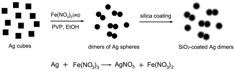
A schematic showing how dimers of Ag nanospheres are formed during etching of Ag nanocubes with an aqueous Fe(NO3)3 solution in ethanol.
Figure 2, A and B, shows typical SEM and TEM images of the Ag nanosphere dimers prepared from Ag nanocubes of ~100 nm in edge length (Figure S1). White and black ellipses were drawn to highlight the dimers in the SEM and TEM images, respectively. It can be seen that a large number of dimers were distributed over a wide area on the substrate, indicating that a significant proportion of the particles in the final product existed in the well-defined dimeric structure. Counting over 150 Ag nanoparticles on the SEM or TEM images, we found that the percentage of dimerization (i.e., the number of dimerized spheres divided by the total number of spheres) was ~66%. The insets in Figure 2, A and B, show magnified SEM and TEM images of the dimers, implying that the dimers had a smooth surface. The magnified TEM image of an individual dimer clearly shows a spherical shape for the two constituent Ag spheres that were 79.4 and 81.1 nm in diameter, respectively. Because the cubes we used for the etching process were single crystals, the resulting nanospheres in the dimers were also single crystals, as confirmed by the uniform contrast across the particle under TEM. This is further supported by the HRTEM image shown in Figure 2C. There was a narrow gap of ~0.67 nm wide between the two nanospheres, forming the so-called hot-spot region. Figure 2D shows a TEM image of the sample after silica coating. Again, a large number of dimers can be easily identified in this sample, clearly demonstrating that the dimers were formed in the reaction solution rather than on the substrate during SEM or TEM sample preparation. The inset in Figure 2D shows a magnified TEM image of an individual silica-coated dimer. The strong contrast difference between Ag and SiO2 suggests that the SiO2 coating had a more or less uniform thickness of ~11.6 nm over the entire surface of the dimer.
Figure 2.
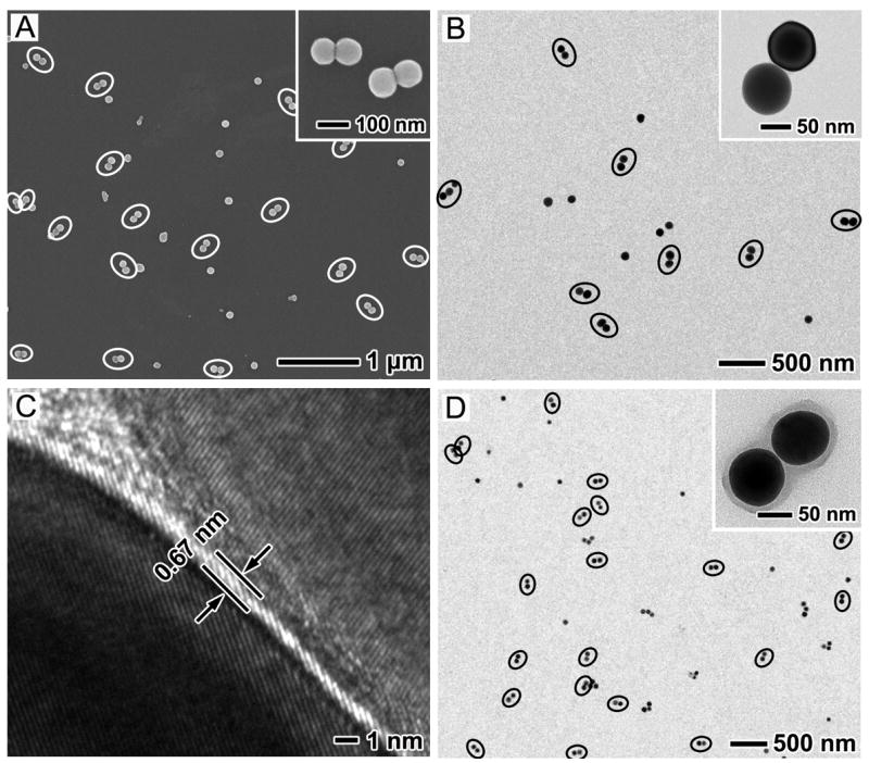
(A) SEM and (B) TEM images of Ag nanosphere dimers prepared from 100-nm Ag nanocubes. (C) HRTEM image of the gap in a dimer and (D) TEM image of the dimers after their surface had been coated with silica. The dimers are highlighted by white and black ellipses in SEM and TEM images, respectively. The inset in each image shows a magnified SEM or TEM image of the same sample. Experimental conditions: 0.01g of PVP, 1.5 mL ethanol, 50 μL of Fe(NO3)3 aqueous solution (10 mM), and etching for 2 h at room temperature.
This etching method of preparing dimers can be extended to Ag nanospheres with a range of different sizes by employing Ag nanocubes of different edge lengths as precursors. Figure 3, A and B, shows typical SEM and TEM images of Ag nanosphere dimers derived from Ag cubes ~82 nm in edge length (Figure S1). Figure 3, C and D, shows SEM and TEM images of dimers fabricated from Ag cubes ~47 nm in edge length (Figure S1). Similar to the dimers shown in Figure 2, a large number of dimers can be easily identified from the SEM and TEM images, as highlighted again by white and black ellipses. The inset in each image shows a magnified SEM or TEM image of the sample, indicating that all of the spheres had a smooth surface and exhibited a round profile. The dimers derived from 82- and 47-nm Ag cubes were consisted of single-crystal spheres approximately 63 and 40 nm in diameter, respectively. Table 1 provides a summary of the major parameters for the different samples. It can be seen that the as-prepared samples all had relatively high percentages of dimerization (>60%), and the gap widths of the dimers all fell into a narrow range of 0.6-0.7 nm.
Figure 3.
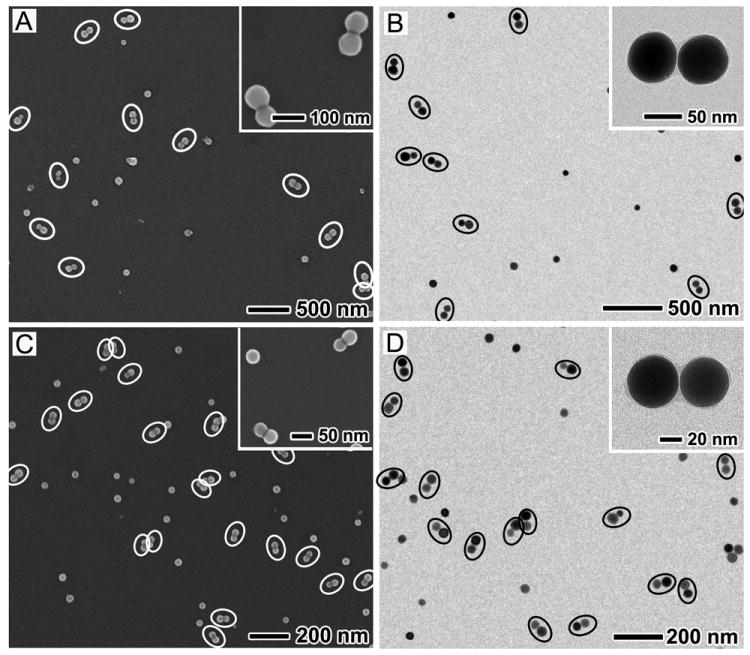
(A, C) SEM and (B, D) TEM images of Ag nanosphere dimers with different sizes prepared from 82-nm and 47-nm Ag nanocubes, respectively. The dimers are highlighted by white and black ellipses in the SEM and TEM images, respectively. The inset in each image shows a magnified SEM or TEM image of the same sample. The 63 nm-dimer was prepared under the same conditions as those in Figure 2, except the use of 82-nm Ag nanocubes. To prepare the 40 nm-dimer, 40 μL of 10 mM Fe(NO3)3 was added and the etching time was 1 h.
Table 1.
A sumamry of the edge length of the Ag nanocubes (lcube), diameter of the resultant spheres in the dimers after etching (dsphere), percentage of dimerization, and width of the gap region in the dimer.
| lcube (nm) | dsphere (nm) | dimerization% | gap width (nm) |
|---|---|---|---|
| 100.4 ± 4.5 | 80.4 ± 4.2 | 66% | 0.67 |
| 82.2 ± 4.5 | 63.0 ± 3.7 | 65% | 0.69 |
| 47.4 ± 3.5 | 39.7 ± 3.4 | 61% | 0.65 |
Figure S2 shows the UV-vis extinction spectra of the cube precursors and the resulting dimers. Four SPR peaks were present for both the 100- and 82-nm cubes, while three peaks can be resolved for the 47-nm cubes. These observations are consistent with the characteristic dipole and quadrupole resonances for Ag nanocubes of these sizes.[11] After wet etching and dimerization, the primary SPR peak of the samples all blue-shifted because of the reduction in size as compared to the corresponding cube precursors. The two peaks located at 350 and 390 nm disappeared due to the higher symmetry of a sphere than a cube. It is worth noting that a shoulder peak appeared at ~500 nm (just next to the primary SPR peak) for the 40-nm Ag sphere dimers, indicative of dimerization. This is consistent with our previous SPR study on dimers consisting of 30-nm Ag spheres.[7] However, the existence of a shoulder peak that implies dimerization could not be resolved from the spectra of dimers made of 80- and 63-nm spheres. This can probably be attributed to the broad SPR peaks for Ag spheres of such large sizes, which could overshadow the shoulder peaks characteristic of dimers.
Interestingly, we found that PVP played an important role in the formation of Ag sphere dimers. The etching reaction could not proceed without the addition of PVP. Figure 4A shows SEM image of the product obtained under the same experimental condition as that for the sample shown in Figure 2 except that no PVP was added. In this case, the resulting product exhibited a cubic shape instead of the spherical morphology, and no dimers could be found. Compared to the precursor cubes, the surface of the cubes shown in Figure 4A was much rougher and there was an obvious coating deposited on the surface. When the reaction time was extended to 18 h, more coating was found on the surface of the cubes and there was still no dimers (Figure 4B), indicating that the etching process was essentially blocked by the coated material. Energy-dispersive X-ray (EDX) analysis was performed in order to identify the composition of the coating on the surface of the nanocubes. Figure 4C displays the EDX spectrum taken from the 18-h sample. In addition to the peak for Si from the substrate and the peak for Ag from the cubes, we also detected the peak for Fe. It is known that Fe(III) ions tend to undergo hydrolysis in an aqueous solution to form iron hydroxide, Fe(OH)3, and the reaction can be described as the following:
| (2) |
Even though the etching process was performed in a medium largely made of ethanol, a small amount of water was introduced into the system when we added the aqueous Fe(NO3)3 solution (40 or 50 μL) and the aqueous suspension of Ag nanocubes (20 μL) into the reaction system. Therefore, formation of Fe(OH)3 during the etching process would be inevitable. Meanwhile, Fe(OH)3 has long been known as a good adsorbent, and is widely used in water purification for entrapping and removing contaminants. Therefore, it can easily adsorb onto the surface of Ag nanocubes. Based on our previous studies, PVP was found to strongly interact with the surface of Ag nanoparticles, with a preferential adsorption on the {100} facets.[12] Since the surface of the cubes are all covered by {100} facets, it is possible that PVP can prevent the adsorption of Fe(OH)3 onto the surface of Ag cubes, thereby facilitating the etching process. In addition, ethanol was also found to be a key component for the successful preparation of the dimers. No dimers was found in our previously reported study when the etching was performed in water even with the addition of PVP.[9b] Some coating was still observed on the surface of the product prepared in water, which was most likely Fe(OH)3. This is because the hydrolysis of Fe(III) ions in water is much more quickly than it is in ethanol. It is not unexpected that much more Fe(OH)3 would be formed when the reaction was performed in water, which subsequently impeded the formation of dimers.
Figure 4.
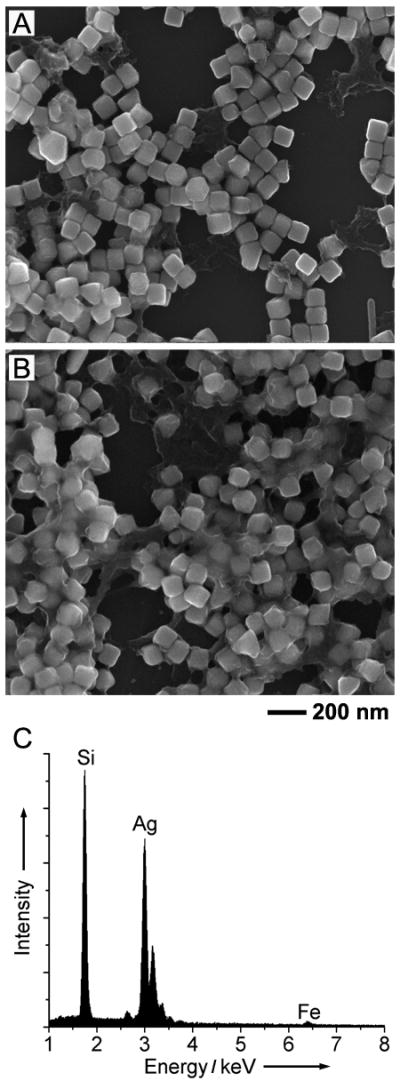
(A, B) SEM images of two samples obtained by wet etching for (A) 1 h and (B) 18 h, respectively. The etching was carried out under the same conditions as those used in Figure 2, except that no PVP was added. (C) EDX spectrum taken from the 18-h sample.
We further performed SERS measurements on the dimers of Ag nanospheres with various sizes. We used 4-methyl-benzenethiol (4-MBT) as the probe molecule because it is known to form a well-defined monolayer on the Ag surface with a characteristic molecular footprint, which is needed for estimating the total number of molecules probed in the SERS measurement and thus for calculating the enhancement factor (EF). In addition, the relatively small size of 4-MBT molecules makes it easier for them to get into the hot-spot region of the dimers. Figure 5 shows the SERS spectra taken from a single dimer of 80-nm Ag spheres, with the laser being polarized parallel (top trace) and perpendicular (middle trace) to the dimer’s long axis. The bottom trace in Figure 5 gives the SERS spectrum recorded from an individual Ag nanosphere. The insets show the corresponding SEM images. The two strong peaks located at 1072 and 1583 cm-1 are the characteristic peaks for 4-MBT. The peak at 1072 cm-1 is due to a combination of the phenyl ring-breathing mode, CH in-plane bending, and CS stretching, and the peak at 1583 cm-1 can be assigned to the phenyl ring-stretching motion (8a vibrational mode).[13] The broad band shown in the middle and bottom trace at 900-1000 cm-1 originated from the Si substrate. In order to compare the SERS spectra recorded for the three different systems in one figure, we amplified the SERS signals by 10 times for the middle and bottom spectra in the plot. It is clear that the intensity of the characteristic 4-MBT SERS peaks decreased in the order of: dimer (parallel) ≫ dimer (perpendicular) > single sphere.
Figure 5.
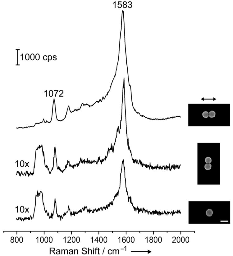
SERS spectra taken from a dimer of Ag nanospheres when the laser polarization was parallel (top trace) and perpendicular (middle trace) to the longitudinal axis of the dimer; and from a single Ag nanosphere (bottom trace). As indicated by “10x”, the intensity of the SERS signals was multiplied by ten times for the middle and bottom traces. The insets show the corresponding SEM images. The scale bar corresponds to 100 nm and is applied to all the images.
We employed the peak at 1583 cm-1 (the strongest band in the spectra) to estimate the EF through the following equation:
| (3) |
where ISERS and Ibulk are the intensities of the same band for the SERS and normal Raman spectra, Nbulk is the number of molecules probed for a bulk sample, and NSERS is the number of molecules probed in the SERS spectrum. The intensities ISERS and Ibulk were determined by the areas of the 1583 cm-1 band. Nbulk was calculated based upon the Raman spectrum of a 0.1 M 4-MBT solution in 12 M NaOH(aq) and the focal volume of our Raman system (1.48 picoL). NSERS was determined according to the assumption that a monolayer of 4-MBT molecules was formed on the Ag surface with a molecular footprint of 0.19 nm2.[14] The NSERS here represents a theoretical maximum number of molecules. Therefore, the actual EF is supposed to be higher than the value reported here. Table 2 summarizes the EFs for dimers of Ag nanospheres with three different sizes with the laser polarization parallel and perpendicular to the dimer’s long axis, as well as the corresponding individual spheres. We can see that the EFs for the dimer decreased with decreasing size for the spheres. In addition, the EFs for dimers with laser polarization parallel to the dimer’s long axis are all much higher than the corresponding ones with the polarization perpendicular to the dimer’s long axis. This result indicates that the SERS signals taken from the dimer were polarization dependent, which is consistent with our previous study on the dimers made of 30-nm Ag spheres.[7] The strong dependence on laser polarization could be attributed to the difference in the electric field enhancements under different excitation directions.[15] When comparing the EF of a dimer and that of a single sphere, we found that the EF of an individual sphere was much lower than that of the corresponding dimer, indicating the hot-spot phenomenon. Besides, the EF (1.7×10⁸) for a dimer of 80-nm spheres with the laser polarization parallel to the dimer’s long axis is almost ten times higher than that of the dimer of 30-nm spheres.[7]
Table 2.
Enhancement factors (EFs) for dimers of Ag nanospheres with the laser polarization parallel (EFdimer-para) and perpendicular (EFdimer-perp) to the dimer’s longitudinal axis, as well as those of the corresponding spheres (EFsphere).
| dsphere (nm) | EFdimer-para | EFdimer-perp | EFsphere |
|---|---|---|---|
| 80.4 ± 4.2 | 1.7 × 10⁸ | 1.5 × 10⁷ | 1.0 × 10⁷ |
| 63.0 ± 3.7 | 9.3 × 10⁷ | 9.2 × 10⁶ | 7.8 × 10⁶ |
| 39.7 ± 3.4 | 3.9 × 10⁷ | 4.6 × 10⁶ | 1.2 × 10⁶ |
In summary, we have successfully prepared well-defined dimers consisting of Ag spheres by etching Ag nanocubes of various sizes. This method can be extended to produce dimers of Ag nanospheres with a wide range of sizes, opening the door for experimental studies on the hot-spot phenomenon in SERS. With 4-MBT as a probe molecule, a SERS EF on the order of 1.7×10⁸ was measured for an individual dimer consisting of 80-nm spheres. We believe that these well-defined dimers are attractive for various applications, including single-molecule detection, plasmonics, sensing, and imaging contrast enhancement.
Experimental Section
The protocols for Ag nanocube synthesis have been reported in detail elsewhere. The 47-nm cubes were synthesized using a sulfide-mediated polyol synthesis.[8b] The 82-nm and 100-nm cubes were prepared using a HCl-mediated polyol synthesis that involved oxidative etching of twinned seeds.[8a] In a typical synthesis of dimers of Ag nanospheres, 0.01 g of poly(vinyl pyrrolidone) (PVP, Aldrich, Mw≈55,000, 04207JD), was dissolved in 1.5 mL of ethanol. Then, a small aliquot of Ag nanocubes (dispersed in water, 20 μL) was added into this ethanol solution. Under magnetic stirring, the nanocube suspension was mixed with 50 μL of 10 mM Fe(NO3)3 (Aldrich, 05713KH) aqueous solution. After the reaction had proceeded at room temperature for 2 h, the product was collected by centrifugation at 10,000 rpm for 5 min and washed three times with ethanol. To prepare the 40 nm-dimer, 40 μL of 10 mM Fe(NO3)3 was added and the etching time was 1 h. The sample was then re-dispersed in ethanol for further characterization.
In a typical process of silica coating on dimers of Ag nanospheres, the as-prepared dimers of Ag nanospheres were mixed with 0.5 mL ethanol; 0.25 mL of this mixture was then transferred to a solution of 0.8 mL ethanol and 20 μL deionized water. Under continuous magnetic stirring, 20 μL of 29% ammonia solution and 10 μL tetraethylorthosilicate (TEOS, Aldrich, 09118DJ) were sequentially added. After the reaction had proceeded at room temperature for 5 h, the solution was centrifuged at 10,000 rpm to isolate the precipitate, which was then re-dispersed in ethanol for further characterization.
Transmission electron microscopy (TEM) images were captured using a Tenai G2 Spirit Twin microscope operated at 120 kV (FEI, Hillsboro, OR). High-resolution TEM images were captured using a field-emission 2100F microscope (JEOL, Tokyo, Japan) operated at 200 kV. Scanning electron microscopy (SEM) images were captured using a Nova NanoSEM 230 field-emission microscope (FEI, Hillsboro, OR) operated at an accelerating voltage of 15 kV. Samples were prepared by dropping an ethanol suspension of the particles on a piece of silicon wafer (for SEM) or carbon-coated copper grid (for TEM). UV-vis extinction spectra were recorded using a UV-visible spectrometer (Varian, Cary 50).
In a typical procedure, samples for correlated SEM and SERS experiments were prepared by drop-casting an ethanol suspension of the sample on a Si substrate that had been patterned with registration marks and letting it dry under ambient conditions. Once the sample had dried, it was rinsed with copious amounts of ethanol, immersed in a 5 mM solution of 4-methyl-benzenethiol (4-MBT; Aldrich) in ethanol for 1 h, taken out, washed with copious amounts of ethanol, and finally dried under a stream of air. All samples were used immediately for SERS measurements after preparation. The SERS spectra were recorded using a Renishaw inVia confocal Raman spectrometer coupled to a Leica microscope with 50x objective (NA=0.90) in backscattering geometry. The 514 nm wavelength was generated with an argon laser coupled to a holographic notch filter with a grating of lines per millimeter. The backscattered Raman signals were collected on a thermoelectrically cooled (-60 °C) CCD detector. The scattering spectra were recorded in the range of 800-2000 cm-1, in one acquisition, 30 s accumulations, and 0.5 mW at the sample.
Footnotes
This work was supported in part by a research grant from the NSF (DMR-0804088) and a 2006 Director’s Pioneer Award from the NIH (DP1 OD000798). P.H.C.C. was also supported in part by the Fulbright Program and the Brazilian Ministry of Education (CAPES). Part of the work was performed at the Nano Research Facility (NRF), a member of the National Nanotechnology Infrastructure Network (NNIN), which is supported by the NSF under ECS-0335765. NRF is part of School of Engineering and Applied Science at Washington University in St. Louis.
References
- 1.a) Cao YC, Jin R, Mirkin CA. Science. 2002;297:1536. doi: 10.1126/science.297.5586.1536. [DOI] [PubMed] [Google Scholar]; b) Alivisatos AP. Nat Biotechnol. 2004;22:47. doi: 10.1038/nbt927. [DOI] [PubMed] [Google Scholar]; c) Pyayt AL, Wiley B, Xia Y, Chen A, Dalton L. Nature Nanotech. 2008;3:660. doi: 10.1038/nnano.2008.281. [DOI] [PubMed] [Google Scholar]; d) Stiles PL, Dieringer JA, Shah NL, Van Duyne RP. Annu Rev Anal Chem. 2008;1:601. doi: 10.1146/annurev.anchem.1.031207.112814. [DOI] [PubMed] [Google Scholar]; e) Banholzer MJ, Millstone JE, Mirkin CA. Chem Soc Rev. 2008;37:885. doi: 10.1039/b710915f. [DOI] [PMC free article] [PubMed] [Google Scholar]
- 2.a) Nie S, Emory SR. Science. 1997;275:1102. doi: 10.1126/science.275.5303.1102. [DOI] [PubMed] [Google Scholar]; b) Kneipp K, Wang Y, Kneipp H, Perelman LT, Itzkan I, Dasari RR, Feld MS. Phys Rev Lett. 1997;78:1667. doi: 10.1103/PhysRevLett.76.2444. [DOI] [PubMed] [Google Scholar]
- 3.a) Le Ru EC, Meyer M, Blackie E, Etchegoin PG. J Raman Spectrosc. 2008;39:1127. [Google Scholar]; b) Wang Z, Pan S, Krauss TD, Du H, Rothberg LJ. Proc Natl Acad Sci. 2003;100:8638. doi: 10.1073/pnas.1133217100. [DOI] [PMC free article] [PubMed] [Google Scholar]; c) Otto A. J Raman Spectrosc. 2002;33:593. [Google Scholar]
- 4.a) Kneipp K, Kneipp H, Itzkan I, Dasari R, Feld M. Chem Rev. 1999;99:2957. doi: 10.1021/cr980133r. [DOI] [PubMed] [Google Scholar]; b) Etchegoin PG, Le Ru EC. Phys Chem Chem Phys. 2008;10:6079. doi: 10.1039/b809196j. [DOI] [PubMed] [Google Scholar]
- 5.a) Glotzer SC, Solomon MJ. Nat Mater. 2007;6:557. doi: 10.1038/nmat1949. [DOI] [PubMed] [Google Scholar]; b) Whitesides GM, Grzybowski BA. Science. 2002;295:2418. doi: 10.1126/science.1070821. [DOI] [PubMed] [Google Scholar]; c) Klajn R, Bishop KJM, Fialkowski M, Paszewski M, Campbell CJ, Gray TP, Grzybowski BA. Science. 2007;316:261. doi: 10.1126/science.1139131. [DOI] [PubMed] [Google Scholar]; d) Rycenga M, McLellan JM, Xia Y. Adv Mater. 2008;20:2416. [Google Scholar]
- 6.a) Alivisatos AP, Johnsson KP, Peng XG, Wilson TE, Loweth CJ, Bruchez MP, Schultz PG. Nature. 1996;382:609. doi: 10.1038/382609a0. [DOI] [PubMed] [Google Scholar]; b) Loweth CJ, Caldwell WB, Peng XG, Alivisatos AP, Schultz PG. Angew Chem Int Ed. 1999;38:1808. doi: 10.1002/(SICI)1521-3773(19990614)38:12<1808::AID-ANIE1808>3.0.CO;2-C. [DOI] [PubMed] [Google Scholar]; c) Park SY, Lytton-Jean AKR, Lee B, Weigand S, Schatz GC, Mirkin CA. Nature. 2008;451:553. doi: 10.1038/nature06508. [DOI] [PubMed] [Google Scholar]; d) Novak JP, Feldheim DL. J Am Chem Soc. 2000;122:3979. [Google Scholar]; (e) Sardar R, Heap TB, Shumaker-Parry JS. J Am Chem Soc. 2007;129:5356. doi: 10.1021/ja070933w. [DOI] [PubMed] [Google Scholar]
- 7.Li W, Camargo PHC, Lu X, Xia Y. Nano Lett. 2009;9:485. doi: 10.1021/nl803621x. [DOI] [PMC free article] [PubMed] [Google Scholar]
- 8.a) Im SH, Lee YT, Wiley BJ, Xia Y. Angew Chem Int Ed. 2005;44:2154. doi: 10.1002/anie.200462208. [DOI] [PubMed] [Google Scholar]; b) Siekkinen AR, McLellan J, Chen J, Xia Y. Chem Phys Lett. 2006;432:491. doi: 10.1016/j.cplett.2006.10.095. [DOI] [PMC free article] [PubMed] [Google Scholar]; c) Skrabalak SE, Au L, Li X, Xia Y. Nature Protoc. 2007;2:2182. doi: 10.1038/nprot.2007.326. [DOI] [PubMed] [Google Scholar]
- 9.a) Lu X, Au L, McLellan J, Li Z, Marquez M, Xia Y. Nano Lett. 2007;7:1764. doi: 10.1021/nl070838l. [DOI] [PMC free article] [PubMed] [Google Scholar]; b) Cobley C, Rycenga M, Zhou F, Li Z, Xia Y. J Phys Chem C. 2009;113:16975. doi: 10.1021/jp8101817. [DOI] [PMC free article] [PubMed] [Google Scholar]
- 10.Evans DF, Wennerström H. The Colloidal Domain: Where Physics, Chemistry, Biology, and Technology Meet. 2. Chapter 8 Wiley; New York: 1999. [Google Scholar]
- 11.Zhou F, Li ZY, Liu Y, Xia Y. J Phys Chem C. 2008;112:20233. [Google Scholar]
- 12.Sun Y, Mayers B, Herricks T, Xia Y. Nano Lett. 2003;3:955. [Google Scholar]
- 13.a) Sauer G, Brehm G, Scheneider S. J Raman Spectrosc. 2004;35:568. [Google Scholar]; b) Osawa M, Matsuda N, Yoshii K, Uchida I. J Phys Chem. 1994;98:12702. [Google Scholar]
- 14.a) Seo K, Borguet E. J Phys Chem C. 2007;111:6335. [Google Scholar]; b) Tao Y-T, Wu C-C, Eu J-Y, Lin W-L, Wu K-C, Chen C-H. Langmuir. 1997;13:4018. [Google Scholar]
- 15.McLellan JM, Li ZY, Siekkinen AR, Xia Y. Nano Lett. 2007;7:1013. doi: 10.1021/nl070157q. [DOI] [PubMed] [Google Scholar]