Abstract
High pulse repetition rate (≥10 GHz) diode-pumped solid-state lasers, modelocked using semiconductor saturable absorber mirrors (SESAMs) are emerging as an enabling technology for high data rate coherent communication systems owing to their low noise and pulse-to-pulse optical phase-coherence. Quantum dot (QD) based SESAMs offer potential advantages to such laser systems in terms of reduced saturation fluence, broader bandwidth, and wavelength flexibility. Here, we describe the development of an epitaxial process for the realization of high optical quality 1.55 µm In(Ga)As QDs on GaAs substrates, their incorporation into a SESAM, and the realization of the first 10 GHz repetition rate QD-SESAM modelocked laser at 1.55 µm, exhibiting ∼2 ps pulse width from an Er-doped glass oscillator (ERGO). With a high areal dot density and strong light emission, this QD structure is a very promising candidate for many other applications, such as laser diodes, optical amplifiers, non-linear and photonic crystal based devices.
Self-assembled In(Ga)As/GaAs quantum dots (QDs) have been investigated for three decades1, and are a mature technique applied to extend the operating wavelength of GaAs based devices to 1.3 μm. Such devices have potentially superior characteristics due to three-dimensional carrier confinement1. So far, ∼1–1.3 µm QDs have been successfully employed in high performance laser diodes2, modelocked lasers3, photo-detectors4, semiconductor saturable absorber mirrors (SESAMs)5, superluminescent light emitting diodes6 and many other commercial optoelectronic devices7. Recently, QDs have emerged as a key technology in ultrafast science and technology3. This is due to extremely broad gain bandwidths offering shorter pulse generation in ultrafast lasers3, and fast carrier dynamics exhibiting picosecond scale recovery of both absorption and gain8. This has given rise to the use of QD absorbers in SESAMs to mode-lock solid-state lasers3, optically pumped vertical extended-cavity surface-emitting lasers9 and fiber lasers10.
Solid-state lasers, fundamentally modelocked using SESAMs, typically exhibit low timing jitter, high pulse-to-pulse phase coherence, and high individual optical spectral mode signal to noise ratio (SNR)11,12 These features are particularly important, but very difficult to achieve at high pulse repetition rates (10 GHz or higher), which are highly desired in applications including ultrahigh speed transmission systems up to 30 Tbits/second13, optical clocking, multi-wavelength sources14, continuum generation and frequency metrology15, to name a few. Coherent optical communications is a rapidly growing field due to the continued exponential growth of consumed energy in non-optical communications servers and networks, as well as the constantly growing need for communication bandwidth. QD-based SESAMs offer many potential advantages for such lasers. In high repetition rate SESAM modelocked lasers16, the pulse energy is very low requiring relatively tight focusing onto the quantum well (QW)-based SESAM in order to achieve saturation. The tight focusing with highly curved intracavity mirrors limits the design freedom for such compact laser cavities. QD technology has the potential to resolve this issue owing to their lower saturation fluence compared to QWs. The additional degree of freedom introduced by variability of the areal QD density allows for low saturation fluence (Fsat) in conjunction with moderate modulation depth (R) to be adjustable independent of each other, while for QW-based devices the product Fsat·R is constant17. In addition, the unique characteristic of large inhomogeneous dot size distribution of QD devices, offers the promise of broader modeleocked laser bandwidth and more flexibility in the laser central operating wavelength.
It is very challenging to fabricate a high performance SESAMs working in 1.55 μm wavelength region18. InP technology dominates the 1.55 µm region, yet InP based QD technology is significantly less mature than that of GaAs. Furthermore, high quality distributed Bragg reflectors (DBRs) are difficult to obtain with InP based materials. In addition, GaAs based materials exhibit a number of advantages; higher thermal conductivity, larger band offsets (reducing thermal sensitivity), larger substrates (reducing device cost), and higher refractive index contrast of lattice matched alloys19. Compared to the development of 1.3 µm GaAs based QDs, the shift to 1.55 µm poses significant challenges in materials science and engineering. Following the introduction of a strained InGaAs cap layer to reach 1.3 µm, pushing the technology to 1.55 µm devices would logically merely require even higher indium content QD capping layers and larger QDs. However, until now there are only a few studies in this direction20. High indium concentration in the QDs and the surrounding matrix very readily induces non-radiative recombination centres which rapidly degrade the crystal and optical quality of the QDs, making such QD materials unsuitable for device applications. Alternative methods to ameliorate this issue are capping InAs/GaAs QDs with quaternary InGaNAs21 or InGaAsSb22 layers, which significantly complicates the epitaxial growth process and is detrimental to the optical and material qualities of the QDs. Emission around 1.5 µm has also been obtained from an InAs/GaAs QD structure grown on thick metamorphic InGaAs buffer layers/virtual substrates23, but repeatability and reliability are significant issues for such structures, as is the difficulty in growing thick lattice-matched alloys or DBRs. The development of high quality 1.55 µm QDs, compatible with other GaAs technologies (e.g. DBRs, photonic crystals) remains a key goal for quantum dot epitaxy research.
In this paper, we describe the development of an epitaxial process for the realization of high optical quality QDs emitting at 1.55 µm. We describe the development of an asymmetric InGaAs/GaAs dot-in-well (DWELL) structure with room temperature PL (RT-PL) comparable to that of 1.3 µm QD structures, and the realization of a working QD-SESAM in this spectral regime. The operation of the QD-SESAM is demonstrated by modelocking a 10 GHz pulse repetition rate Er-doped laser generating 2.4 ps pulses at 1.55 µm central wavelength.
Results
Five InGaAs/GaAs QD test structures were grown by solid-source molecular beam epitaxy (MBE). Sample A, B, and C were DWELL structures consisting of a 1 nm lower, and 6 nm upper QW layers of In0.31Ga0.69As, In0.35Ga0.65As, and In0.39Ga0.61As, respectively. The band-structure of this hetero-structure, termed a symmetric DWELL, is shown schematically in band diagram a in Fig. 1(a). Figure 1(b) shows RT-PL spectra obtained from the structures. With increasing In% in the InGaAs QWs, the emission wavelength is red-shifted from 1552 nm in sample A to 1592 nm in sample B, along with a reduction in PL peak intensity. A weak PL signal was detected from sample C. In sample D, the InAs QDs were directly grown on a GaAs layer and covered by a 6 nm In0.31Ga0.69As layer, for which the PL peak wavelength is at ∼1540 nm. However, the PL intensity is weaker than that of sample A. For sample E, the QDs were positioned in an asymmetric InGaAs QW pair with 1 nm lower In0.18Ga0.82As layer and 6 nm upper In0.31Ga0.69As layer, as shown in the diagram b, in Fig. 1(a). The emission peak is at 1565 nm for sample E, and the optical quality is improved (2.5 times PL intensity enhancement and >10% PL emission linewidth narrowing). From the inset to Fig. 1(b) the RT-PL peak/integrated intensity was found to be only ∼15 times/4 times lower in sample E compared to a 1.3 µm QD test sample (a DWELL structure with 1 nm In0.18Ga0.82As underneath layer and 6 nm In0.18Ga0.82As over-growth layer of InAs QD layer). This highlights the high crystal perfection and high material quality for this growth technique, significantly better than other previous reports, where the PL peak intensity of the QDs became much weaker when the emission wavelength was shifted from 1.3 µm to 1.5 µm24.
Figure 1. (a) Schematic band diagram for InAs QD inserting in a symmetric and an asymmetric InGaAs QW pairs; (b) Room temperature PL spectra of different 1.55 µm InAs QD structures under identical excitation power of 120 mw.
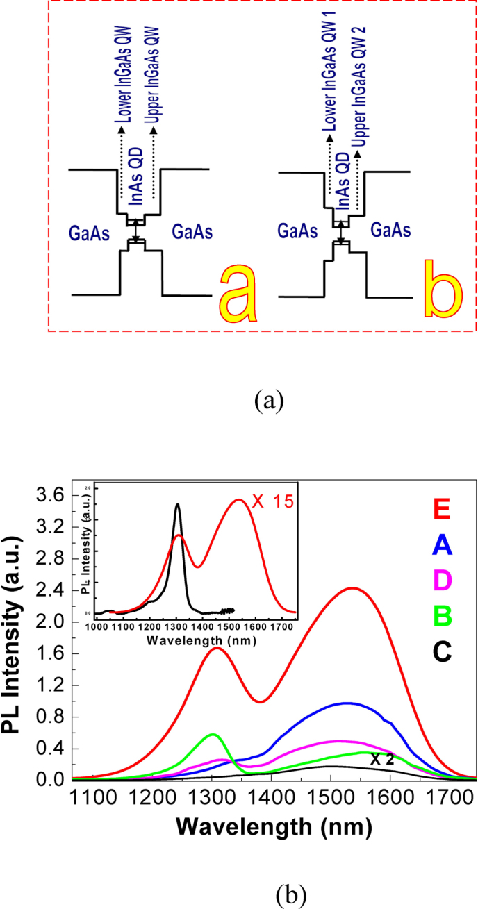
Inset: a comparison of room temperature PL characteristics between a 1.3 µm QD sample and a 1.55 µm QD sample.
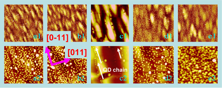
Five un-capped QD samples were grown under identical conditions as discussed previously for AFM measurement. Fig. 2: a1, b1, c1, d1 and e1 show 5×5 µm2 AFM images corresponding to QD samples A, B, C, D, and E, respectively. A number of mounds and ridges are observed along the [0–11] direction on the sample surface in Fig. 2: a1 and b1. This becomes much more pronounced as shown in Fig. 2: c1, while in Fig. 2: d1 and e1, the anisotropic crystallographic alignments become weaker, with much smoother surfaces being obtained. Nucleation on a smooth surface is known to be a key factor to suppress the formation of dislocations during QD growth25.
Figure 2. a1, b1, c1, d1, and e1 are 5×5 µm2 atomic force microscopy (AFM) images, and a2, b2, c2, d2, and e2 are 1×1 µm2 AFM images of sample A, B. C, D, and E, respectively.
Details of the dot density, size and distribution are acquired in Fig. 2: a2, b2, c2, d2 and e2, which are 1×1 µm2 AFM images corresponding to QD samples A, B, C, D, and E respectively. The comparatively high dot density of ∼4.0×10¹⁰/cm2 is achieved in a2, b2 and e2 indicating that the lower InGaAs QW layer provides additional nucleation positions for the QD growth, which is further confirmed by the relative low dot density of ∼2.8×10¹⁰/cm2 in Fig. 2: d2, in which the InAs QD is grown directly on a GaAs layer. The lowest dot density is found to be 3.8×10⁹/cm2 in Fig. 2: c2. Referring to the 5×5 µm2 AFM image in Fig. 2: c1, this is caused by the very low In sticking coefficient on the highly non-planar surface. Interestingly, periodic QD chains situated at the edges of the ridges along the [0–11] direction are observed in Fig. 2: c2. This QD ordering is attributed to the accumulation of the highly anisotropic strain field on the InGaAs/GaAs surface. This is a different approach, but equally satisfactory in results as other techniques26 of InAs QDs grown on GaAs (100) or high stepped vicinal substrates to obtain correlated QD chains, of possible use in a range of novel optical and electronic devices applications27.
There are two obvious dot size distributions observed in Fig. 2: a2 and b2, in which the height/width of regular dots is ∼7 nm/∼40 nm, and for “giant” dots is ∼20 nm/∼100 nm. These giant dots are due to the rough surface of the lower InGaAs layer providing a disordering of the nucleation centres for the QDs growth leading to individual dots coalescing. This can be expected to result in the appearance of dislocations due to coalesced dots being relaxed28. The giant dots are also observed in Fig. 2: e2, but as the surface in the lower InGaAs layer is smoother, the areal density is much smaller than that in Fig. 2: a2 and b2, and the dot size distribution is more uniform. Combined with the results of dot density, this can well explain the PL results in Fig. 1(b) for these 1.55 µm QD samples. For sample E, a high areal QD density, more homogeneous dot size distribution, and small number of coalesced QDs is observed, leading to the highest optical quality.
In addition to the QD active region, there are generally thick cladding layers for optical/carrier confinement in most devices, so it is necessary to investigate the thermal stability of the 1.55 µm DWELL structures as typical growth temperature for these layers are higher than that for QD growth. As seen in Fig. 3(a), by using a growth temperature of ∼565°C for the upper AlGaAs cladding layer growth, the QDs exhibit high material quality. However, by raising the growth temperature to 585°C for the AlGaAs cladding layer growth, threading dislocations are observed as seen in Fig. 3(b). Threading dislocations also appeared in Fig. 3(c), in which the epitaxial growth conditions are the same as that in the sample in Fig. 3(a), but with the sample undergoing a post-growth rapid thermal annealing (RTA) treatment. These results indicate that as the QDs endure a high strain environment due to the large In% in the 1.55 µm DWELL structures, dislocations are easily formed by inducing additional elastic stress by high temperature growth or annealing. This suggests that these 1.55 µm QDs are sensitive to temperature though they were grown at a comparatively high temperature. This result is rather different from that obtained in previous work on short emission wavelength (1 µm or 1.3 µm) QDs where the QDs grown at higher temperature exhibited good thermal stability29. Therefore, besides the QD active region epitaxy, careful control of the growth parameters, especially the growth temperature, for cladding layers is another key factor to realize high quality QD device structures for 1.55 µm photonic applications.
Figure 3. The comparison of dark filed (002) cross-sectional transmission electron microscopy (TEM) images for different 1.55 µm QD samples.
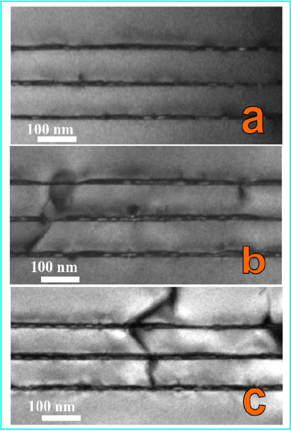
a: QDs capped by a AlGaAs overgrowth layer grown at 565°C; b: QDs capped by a AlGaAs overgrowth layer grown at 585°C; c: QDs capped by a AlGaAs overgrowth layer grown at 565°C with RTA treatment.
Discussion
Based on these structures, a 1550 nm GaAs based In(Ga)As QD-SESAM has been fabricated, and implemented in a 10 GHz pulse repetition rate laser. The cross-sectional TEM image of the QD-SESAM is shown in Fig. 4(a). The QD-SESAM is characterized with a precision saturation fluence (Fsat) measurement system30 and exhibits a nonlinear modulation depth of 0.4%, and a saturation fluence of 9 µJ/cm2. For comparison, the QW-SESAM was characterized with the same precision system and exhibits a nonlinear modulation depth of 0.5%, saturation fluence of 15 µJ/cm2, and nonsaturable losses of 0.1%. When operated with the QD-SESAM, the laser shows a lower lasing threshold compared to that when operating with a standard QW-SESAM, suggesting that the QD-SESAM’s nonsaturable losses are 0.1% or lower.
Figure 4.
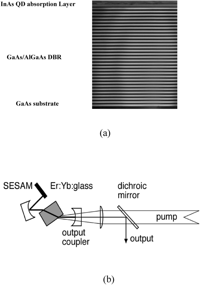
(a) Cross-sectional TEM image of the 1.55 µm QD-SESAM. (b)10 GHz ERGO laser layout. The gain medium is Er:Yb doped glass and QD-SESAM is placed at the end of the cavity.
The standard ERGO laser (Fig. 4(b)) is a V-cavity consisting of an output coupler, Er:Yb doped glass as a gain medium, a fold mirror, and a QW-SESAM31. The laser is fundamentally modelocked, meaning that only one pulse is circulating within the cavity. The cavity length is slightly less than 15 mm. Passive fundamental modelocking with the SESAM enables ultralow pulse timing jitter and pulse-to-pulse optical phase coherence, which is essential for high data rate communication systems with coherent modulation formats.
In our experiment, the QW-SESAM is replaced with the QD-SESAM described above and the output is displayed in Fig. 5. The average output power of the modelocked laser is 8 mW, using 130 mW of pump power. The modelocked spectral FWHM is 1.4 nm and the pulse duration is 2.4 ps, assuming sech2 pulse shape. The Q-switching threshold is at 70 mW of pump power. The pulse duration and the output power are in the same range (1.9 ps, 12 mW and 2.4 ps, 8 mW for QW and QD respectively) for the QW and QD-SESAM modelocked 10 GHz ERGO lasers. Critically, using the QD-SESAM, the measured Q-switching threshold is halved. This opens the route for the development of higher frequency modelocked lasers.
Figure 5.
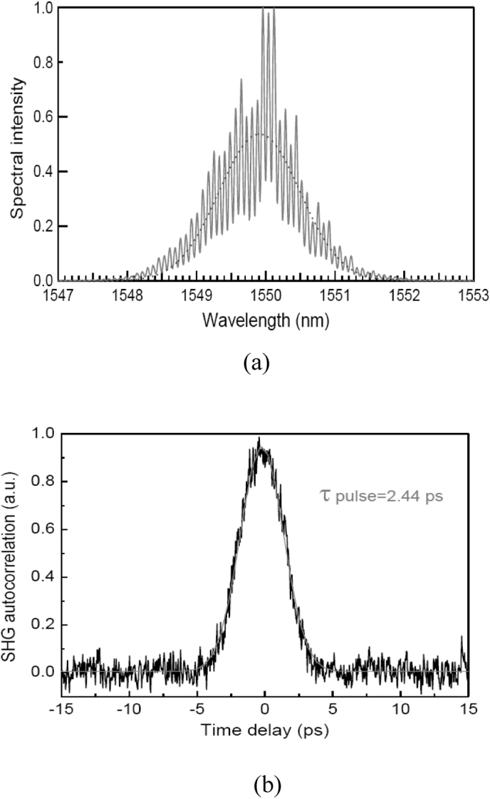
(a) 10 GHz ERGO laser output: optical power spectrum and (b) second harmonic generation (SHG) autocorrelation trace. The spectrum is fitted to a Gaussian curve with FWHM = 1.4 nm. The SHG autocorrelation trace is fitted to sech2 pulse autocorrelation and the deconvolved.
In conclusion, InAs QDs inserted in an asymmetric InGaAs QW structure has been demonstrated to significantly improve the material and optical quality of 1.55 µm In(Ga)As/GaAs QDs, and hence the QD-SESAM. This has allowed us to realize the first 10 GHz repetition rate QD-SESAM modelocked laser operating at 1550 nm. The lower Q-switching threshold suggests the potential to increase the beam waist diameter on the SESAM in an improved and possibly simpler laser design, enabling simpler manufacturing of higher repetition rate (e.g. >25 GHz) fundamentally modelocked lasers, highly desired in telecom and other applications.
Methods
Crystal growth: The epitaxial materials were fabricated by solid-source III-V MBE on semi-insulating GaAs (100) substrates. Each QD test sample contains three DWELL layers, which separated by 60 nm GaAs spacer layer. Each DWELL layer consists of 2.9 monolayer (ML) InAs QDs inserted into different InGaAs QW pairs with 1nm InGaAs underneath layer and 6nm InGaAs over-growth layer. The QD-SESAM contains one DWELL layer grown on a bottom DBR mirror consisting of 31 pairs of un-doped GaAs (115nm) and Al0.98Ga0.02As (134nm) layers. The growth temperature was 530°C for In containing layers, and 565°C for GaAs layers.
Post-growth intermixing process: The RTA process was performed in an N2 ambient at a temperature of 650°C for 15 seconds using a GaAs proximity cap.
Measurements: PL measurements were performed at room temperature with a solid state laser, emitting at 532 nm. The PL emission was detected using a InGaAs detector. AFM measurements were performed with a Nanoscope Dimension™ 3100 SPM AFM system in ambient conditions using a noncontact mode. TEM measurements were performed using a 200KeV JEOL-2010 microscope by Integity Scientific Ltd. The ultrafast laser measurements were performed with the Femtochrome Research autocorrelator, model 103XL, and Agilent optical spectrum analyzer, model 86142B.
Author Contributions
Z. Z developed and performed the overall material epitaxy growth. Z. Z and R. H. guided the material characterization and analysis. K. Z. and Q. W. were involved with the PL and AFM measurements. A. O., K. W. and U. K. designed the QD-SESAM; B. R. obtained the 10 GHz laser results and wrote the laser part of the manuscript; S. K. built the 10 GHz laser, and M. M., A. O. and T. S. characterized the QD-SESAMs with Fsat setup. All authors assisted with preparation of the manuscript and discussed the results.
Acknowledgments
This work was supported by EU FP7 project FastDot, under grant agreement number 224338.
References
- Arakawa Y. & Sakaki H. Multidimensional quantum well laser and temperature-dependence of its threshold current. Appl Phys Lett 40, 939–941 (1982). [Google Scholar]
- Deppe D. G., Shavritranuruk K., Ozgur G., Chen H. & Freisem S. Quantum dot laser diode with low threshold and low internal loss. Electron. Lett. 45, 54–55 (2009). [Google Scholar]
- Rafailov E. U., Cataluna M. A. & Sibbett W. Mode-locked quantum-dot lasers. Nature Photon 1, 395–401 (2007). [Google Scholar]
- Wu J. et al. Intersublevel Infrared Photodetector with Strain-Free GaAs Quantum Dot Pairs Grown by High-Temperature Droplet Epitaxy. Nano Letters 10, 1512-1516 (2010). [DOI] [PubMed] [Google Scholar]
- Keller U. Recent developments in compact ultrafast lasers. Nature 424, 831–838 (2003) [DOI] [PubMed] [Google Scholar]
- Zhang Z. Y., Hogg R. A., Lv X. Q. & Wang Z. G. Self-assembled quantum-dot superluminescent light-emitting diodes. Adv. Opt. Photon 2, 201–228 (2010). [Google Scholar]
- Sugawara M. & Usami M. Quantum dot devices handling the heat. Nature Photon 3, 30–31 (2009). [Google Scholar]
- Borri P., Schneider S., Langbein W. & Bimberg D. Ultrafast carrier dynamics in InGaAs quantum dot materials and devices. J ournal of Optics A-Pure and Applied Optics 8, S33–S46 (2006). [Google Scholar]
- Maas D. J. H. C. et al. Vertical integration of ultrafast semicondcutor lasers. Appl. Phys. B 88, 493–497 (2007). [Google Scholar]
- Herda R. et al. Semiconductor quantum-dot saturable absorber mode-locked fiber laser. IEEE Photonics Technology Letters 18, 157–159 (2006). [Google Scholar]
- Schlatter A. et al. Nearly quantum-noise-limited timing jitter from miniature Er:Yb:glass lasers. Opt. Lett. 30,1536–1538 (2005). [DOI] [PubMed] [Google Scholar]
- Sudmeyer T. et al. Femtosecond laser oscillators for high-field science. Nature Photon 2, 599–604 (2008). [Google Scholar]
- Hillerkuss D. et al. 26 Tbits/s line-rate super-channel transmission utilizing all-optical fast Fourier transform processing. Nature Photon 5, 364–371 (2011). [Google Scholar]
- Bakopoulos P. et al. Multi-wavelength laser source for dense wavelength division multiplexing networks. Proceedings of Optical Fiber Communications Conference, paper OWJ2 (2007). [Google Scholar]
- Bartels A., Heinecke D. & Diddams S. A. 10-GHz self-referenced optical frequency comb. Science 326, 681–682 (2009). [DOI] [PubMed] [Google Scholar]
- Oehler A. E. H., Suedmeyer T., Weingarten K. J. & Keller U. 100 GHz passively mode-locked Er:Yb:glass laser at 1.5 μm with 1.6-ps pulses Opt. Express 16, 21930–21935 (2008). [DOI] [PubMed] [Google Scholar]
- Maas D. J. H. C. et al. Growth parameter optimization for fast quantum dot SESAMs. Opt. Express 16, 18646–18656 (2008). [DOI] [PubMed] [Google Scholar]
- Wang F. et al. Wideband-tuneable, nanotube, mode-locked, fibre laser. Nature Nanotech 3, 738–742 (2008). [DOI] [PubMed] [Google Scholar]
- Mikhrin V. S. et al. InAs/InGaNAs/GaNAs QW and QD heterostructures emitting at 1.4-1.8µm. Semiconductors 40, 342–345 (2006). [Google Scholar]
- Seravalli L., Frigeri P., Trevisi G. & Franchi S. 1.59 mu m room temperature emission from metamorphic InAs/InGaAs quantum dots grown on GaAs substrates. Appl Phys Lett 92, 213104 (2008). [Google Scholar]
- Richter M., Damilano B., Massies J., Duboz J. Y. & Wieck A. D. InAs/In0.15Ga0.85As1-xNx quantum dots for 1.5 mu m laser applications. Progress in Semiconductor Materials V-Novel Materials and Electronic and Optoelectronic Applications 891, 185–190 (2006). [Google Scholar]
- Ripalda J. M. et al. Room temperature emission at 1.6 mu m from InGaAs quantum dots capped with GaAsSb. Appl Phys Lett 87, 202108 (2005). [Google Scholar]
- Ledentsov N. N. et al. High performance quantum dot lasers on GaAs substrates operating in 1.5 mu m range. Electron. Lett 39, 1126–1128 (2003). [Google Scholar]
- Sopanen M., Xin H. P. & Tu C. W. Self-assembled GaInNAs quantum dots for 1.3 and 1.55 mu m emission on GaAs. Appl Phys Lett 76, 994–996 (2000). [Google Scholar]
- Liu H. Y. et al. Improved performance of 1.3 mu m multilayer InAs quantum-dot lasers using a high-growth-temperature GaAs spacer layer. Appl Phys Lett 85, 704–706 (2004). [Google Scholar]
- Wang Z. M., Holmes K., Mazur Y. I. & Salamo G. J. Fabrication of (In,Ga)As quantum-dot chains on GaAs (100). Appl Phys Lett 84, 1931–1933 (2004). [Google Scholar]
- Springholz G., Holy V., Pinczolits M. & Bauer G. Self-organized growth of three-dimensional quantum-dot crystals with fcc-like stacking and a tunable lattice constant. Science 282, 734–737 (1998). [DOI] [PubMed] [Google Scholar]
- Ebiko Y. et al. Island size scaling in InAs/GaAs self-assembled quantum dots. Physical Review Letters 80, 2650–2653 (1998). [Google Scholar]
- Chu L., Arzberger M., Bohm G. & Abstreiter G. Influence of growth conditions on the photoluminescence of self-assembled InAs/GaAs quantum dots. Journal of Applied Physics 85, 2355–2362 (1999). [Google Scholar]
- Maas D. J. H. C. et al. High precision optical characterization of semiconductor saturable absorber mirrors. Opt. Express 16, 7571–7579 (2008). [DOI] [PubMed] [Google Scholar]
- Krainer L. et al. Tunable picosecond pulse generating-laser with a repetition rate exceeding 10 GHz. Electron. Lett. 38, 225–227 (2002). [Google Scholar]


