Abstract
The electromechanical performance of piezoelectric scanning mirrors for endoscopy imaging is presented. The devices are supported by a single actuating cantilever to achieve a high fill factor, the ratio of mirror area to the combined mirror and actuator area. The largest fill factor devices (74%) achieved 10° mechanical scan range at +/−10V with a 300 μm long cantilever. The largest angular displacement of 30° mechanical scan range was obtained with a 500 μm long cantilever device with a 63% fill factor driven at 40 Vpp. A systematic investigation of device performance (displacement and speed) as a function of fabrication and operational parameters including the stress balance in the cantilever revealed unexpectedly large displacements with lack of inversion at the coercive field. An interpretation of the results is presented based on piezoelectric film domain orientation and clamping with supporting piezoelectric film characterization measurements.
Keywords: piezoelectric actuator, micromirror, optical scanner, bi-directional scanning, PZT
1. Introduction
A variety of optical imaging techniques are being investigated for optical biopsy applications with the goal of non-invasive rapid identification of precancerous and cancerous growth in the epithelial layer of tissue. These techniques include multiphoton fluorescence, confocal microendoscopy and optical coherence tomography (OCT) [1, 2]. Clinical implementation of these techniques in a endoscope generally requires some form of laser beam scanning, which has been demonstrated with MEMS mirrors at the distal end of the probe (e.g. confocal [3]), multiphoton [4], OCT [5]) or fiber scanning approaches (multiphoton [6], OCT [7]).
Among MEMS mirrors, electrostatically actuated devices offer high speed, but provide limited mechanical scanning range at non-resonance (typically 2–3°) and have a large actuator footprint [3, 4, 8]. Electrothermal mirrors have been extensively investigated in both single bender [9] and 2D scanning configurations [10, 11] and achieve large scanning angles (up to ± 30°) at low driving voltages at the expense of high driving current, the requirement for thermal isolation of the actuator, and often a poor temporal response.
The fabrication and characterization of piezoelectric cantilevered mirrors designed by our group for endoscopic forward looking OCT was described recently [12]. These actuated mirrors feature a large fill factor (mirror/(mirror + actuator) areas) because, unlike two-axis configurations, the mirror is supported on only one side. The fabrication approach improved on previously reported piezoelectric devices [13, 14] by separately defining the actuator arm and optical mirror thickness: a 12 μm mirror thickness provided flatness for optical performance while a thin short actuator arm enabled a large scanning range under sub-resonant conditions. A similar fabrication approach was later used by others to demonstrate a two-dimensional rastering piezomirror [15, 16]. This device enables both bending and torsional actuation modes, however it achieves adequate scanning range only at resonance frequency operation. Operation in sub-resonance regime is highly desirable for exploiting piezomirrors in endoscopic biomedical applications, where a low (tens of Hz), arbitrary scanning speed is convenient to optimize signal-to-noise with suitable integration times. The first generation piezoelectric mirror devices met the designed scanning range of ±6° (equivalent to +/− 12° optical) providing for an adequately sized image (~1 mm). The mirror operated in sub-resonance condition with a stable low frequency response and resonance frequency in the hundreds of Hz.
The aim of this paper is to explore the performance limits of the devices and to establish the trade-offs between scanning range, speed and driving conditions. In piezoelectric cantilevers the scanning range linearly increases with the cantilever length; however, increased length negatively impacts the time response of the device and the fill factor. A systematic investigation of the performance (displacement and speed) as a function of several fabrication and operational parameters including the effect of stress balance in the cantilever, DC offset in the driving voltage and piezoelectric layer thickness is reported. The electrical reliability of the devices was also improved by implementing a crucial modification of the electrical isolation layer which enables application of larger voltages. Unexpectedly large displacements were observed with lack of inversion at the coercive field. An interpretation of the results is presented based on piezoelectric film domain orientation and clamping, and this model was verified with piezoelectric film characterization measurements.
The overall goal was an optimization of the devices for endoscopic imaging applications which require large scanning angle (≥10°) in sub-resonance condition with as compact an actuator as possible.
2. Experimental Procedures
2.1 Design
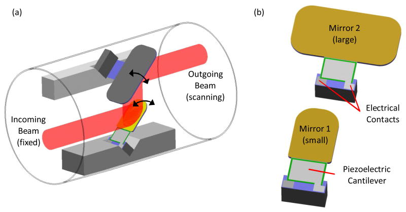
The mirrors were designed to provide forward-looking two-dimensional scanning of a 500 μm diameter beam within a 2.9 mm inner diameter catheter in the cascaded configuration shown in figure 1. Each mirror is actuated in one dimension by a piezoelectric cantilever extending from one side of the mirror. This actuator configuration provides a large ratio of optical aperture to device size. Mirror sizes were chosen to ensure that the light beam is intercepted by the scanning mirrors at any scan position within a 10° mechanical angle range. The first mirror on the beam path is 600 μm × 840 μm and the second one is 1600 μm × 840 μm. The total die size is approximately 1mm × 2mm for the small mirror and 1.6mm × 2mm for the large mirror. For convenience, larger dice (5mm × 5mm) with two mirrors were used for electromechanical evaluation of devices.
Figure 1.
(a) Conceptual schematic of a dual-mirror cascade configuration packaged inside a 2.9mm inner diameter catheter. (b) Drawings of the two component mirrors.
A detailed discussion of the design considerations for the cantilever is found in [12]. Briefly, scanning range is expected to increase with longer cantilever length and smaller PZT thickness. Devices of each mirror size were fabricated with cantilever lengths of 300, 400, and 500 μm. For the 600 μm × 840 μm mirrors, the cantilever width was 600 μm. For the 1600 μm × 840 μm mirrors, the cantilever width ranged from 600 to 1600 μm. PZT thicknesses of 0.64μm and 0.96 μm were investigated.
2.2 Fabrication
Devices were fabricated on 100 mm silicon wafers with 2500 A – 4000 A thermal oxide. The front side process sequence formed the piezoelectric actuator and the reflective mirror. A Ti/Pt layer was deposited by electron beam evaporation. For the piezoelectric layer, Pb(Zr0.53Ti0.47)O3 (PZT) was spin-coated from metal organic precursors (as in [17]) in 80 nm layers and annealed at 700°C for 5 minutes after every two layers for total thicknesses of 0.64 – 0.96 μm. The PZT was patterned using a wet etch (10 H2O:10 HCl: 1 HF), and the Ti/Pt layer was patterned by argon ion milling to form the bottom electrode. Next, an insulator was deposited to prevent shorting between the top and bottom metal layers. In the previously reported devices [12], PECVD of silicon dioxide was used for this isolation layer; however, it did not provide adequate step coverage at the edge of the PZT and was replaced with spin-coated benzocyclobutene (BCB, CYCLOTENE 4022, Dow Chemical Co.). A photoimageable BCB was used to pattern and remove this layer from both the actuation cantilever and the mirror. The top actuation electrode was deposited by electron beam evaporation of Ti/Au/Ti and patterned with a standard photoresist liftoff process. Silicon nitride was deposited by PECVD in order to alter the stress in the cantilever portion of the device. The thickness of this layer influences the native tilt of the mirrors as discussed in detail in section 2.3. To form the reflective mirror surface, Ti/Au was deposited and patterned in a photoresist liftoff process followed by conformal vapor deposition of parylene-C over the entire top surface of the wafer to protect the mirror surface during processing of the back sides of the wafers.
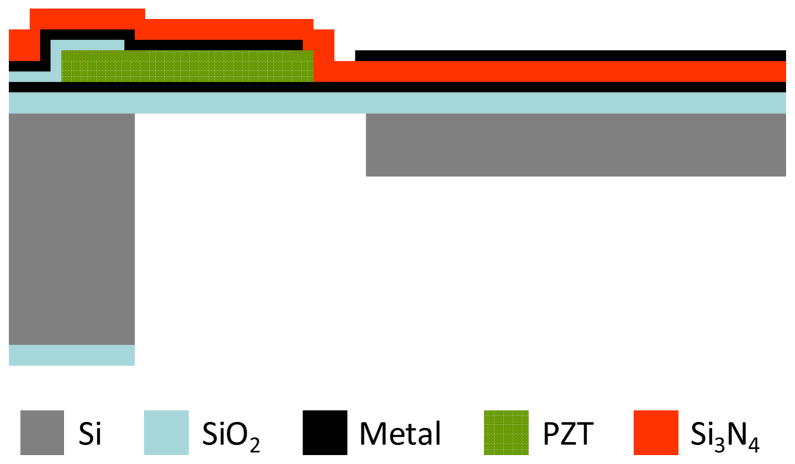
A two-step deep reactive ion etch (DRIE) process was used on the backsides of the wafers to completely remove the silicon from underneath the cantilever portion of the devices for maximum actuation capability while leaving a controlled thickness of silicon underneath the mirror portion of the devices for acceptable mirror flatness. The process used a photoresist mask for the first etch and an oxide mask for the second etch. In the first etch, the areas underneath the cantilever and surrounding the mirror were given a 10–15 μm “head start.” In the second etch, the remainder of the silicon was etched to clear the silicon from underneath the cantilever and to release the devices from the surrounding substrate. Dry film photoresist (Dupont MX 5020) was laminated on the front side of the wafer prior to the final silicon etch to prevent the cantilevers from bending during the etch. The dry film resist was removed with oxygen RIE after completion of the silicon etch. A cross-section of the final device structure is shown in figure 2.
Figure 2.
Illustration of the device cross section.
2.3 Stress balance and native tilt
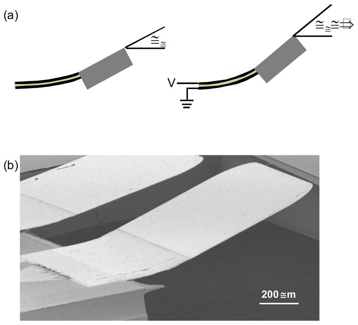
In the absence of any stress compensation, the cantilevers have a significant upward curl due to the combination of the compressive thermal oxide base layer and the tensile PZT and platinum layers. The curvature is typically so severe that the cantilevers break during the release process when no stress balancing layers are applied. The addition of a compressive silicon nitride layer to the top of the cantilever stack has been used to successfully balance the film stresses to produce devices with minimal curvature. The appropriate thickness of silicon nitride was estimated using finite element analysis (FEA). If the silicon nitride layer is not thick enough or compressive enough, then the cantilevers have an upward curl. The curl in the cantilever translates to an angular tilt in the mirror as shown in figure 3a. The native tilt is defined as α0 and the angular displacement due to voltage application is defined as α. Because the mirrors can move in both directions from the native position, α can be positive or negative. This behavior is in contrast to electrothermally actuated mirrors which have significant native tilt and move in only one direction from the native position [18]. An SEM image of a 1600 μm × 840 μm mirror with upward tilt is shown in figure 3b.
Figure 3.
(a) Illustration of the native tilt (α0) and the angular displacement (α) due to voltage application. (b) Scanning electron microscope image of a device with an upward tilting 1600 μm × 840 μm mirror.
The stress state of the cantilever impacts the piezoelectric properties of the PZT layer. In order to determine the effect of the stress state on device performance, we fabricated mirrors that were fully compensated and mirrors that were undercompensated with tilt angles α0 greater than 45°.
2.4 Optomechanical characterization
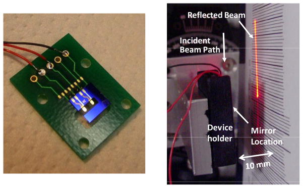
The mirrors were mounted onto custom printed circuit boards to facilitate electrical and mechanical connection to the test apparatus for measurement of angular displacement as shown in figure 4. A He-Ne laser was reflected off the mirror positioned on the rotation axis of a goniometer stage. The mirror reflection was detected with a position sensitive detector (OnTrack) and digitized together with mirror driving voltage from a function generator. The OnTrack detector was removed from its case to reduce the distance between the scanning device and the detector to enable measurement of mechanical scanning angles up to 18°. Displacement measurements were performed in static conditions by applying a DC voltage and in near static condition by applying 1Hz triangular waves with varying amplitudes and offset. Because application of an offset voltage modifies the angular position of the devices, mechanical rotation of the device holder was used to ensure the signal from the entire scan range was within the detector acceptance. The zero angle value in the angular scanning range plots was obtained by appropriate subtractions independent of native tilt and holder orientation. For static measurements, zero angle indicates the position prior to voltage application. For scanning measurements, zero angle indicates the position at the dc offset voltage.
Figure 4.
(a) Photograph of a die containing two mirrors mounted on a printed circuit board for ease of testing. (b) Photograph of measurement setup using a mirror with high native tilt (~ 45°). The mirror is scanning a laser beam at 15 Hz so that the scanned beam appears as a solid line.
For mechanical angular measurements above 18°, the position sensitive detector was removed and a paper screen was used to determine the angular scan range. Exploiting the fact that the amplitude in our devices is constant in low frequency range, the measurements on the screen were conveniently performed at 15 Hz, where the scanning laser beam forms a line whose length can be measured as a function of peak-peak driving voltage. The screen calibration was based on the detector values measured at low drive voltages (e.g. 10 or 20 Vpp).
Polarization hysteresis loops were measured with a ferroelectric tester (Precision Workstation, Radiant Technologies), and capacitance was measured with an LCR meter (Agilent model 4824).
3. Result and Discussions
Performance was compared for devices with full stress compensation (minimal native tilt) and devices with undercompensated stress (upward native tilt). We have demonstrated fabrication and actuation of small (600 μm × 840 μm) and large (1600 μm × 840 μm) sized mirrors and did not observe significant differences in their actuation performance. Cantilever displacement was evaluated under DC and low frequency AC actuation. Because the devices have a flat frequency response below resonance (shown later in figure 12), the DC and low frequency AC displacements are in close agreement. Unless stated otherwise, data was acquired with a 1 Hz triangular driving waveform. Downward tilt is defined as a negative angle α, and upward tilt is defined as a positive angle.
Figure 12.
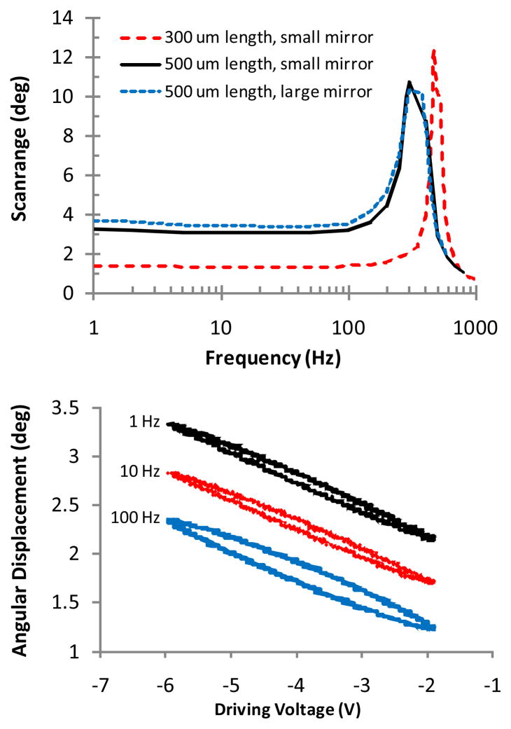
(a) Dynamic response of three different cantilevers indicating the resonance peaks. (b) Angular displacement in response to 4 Vpp triangular driving waveforms with varying frequency. The measured device had a 300 μm long cantilever and large upward tilt. Traces are offset for clarity.
3.1 Relationship between native tilt and displacement
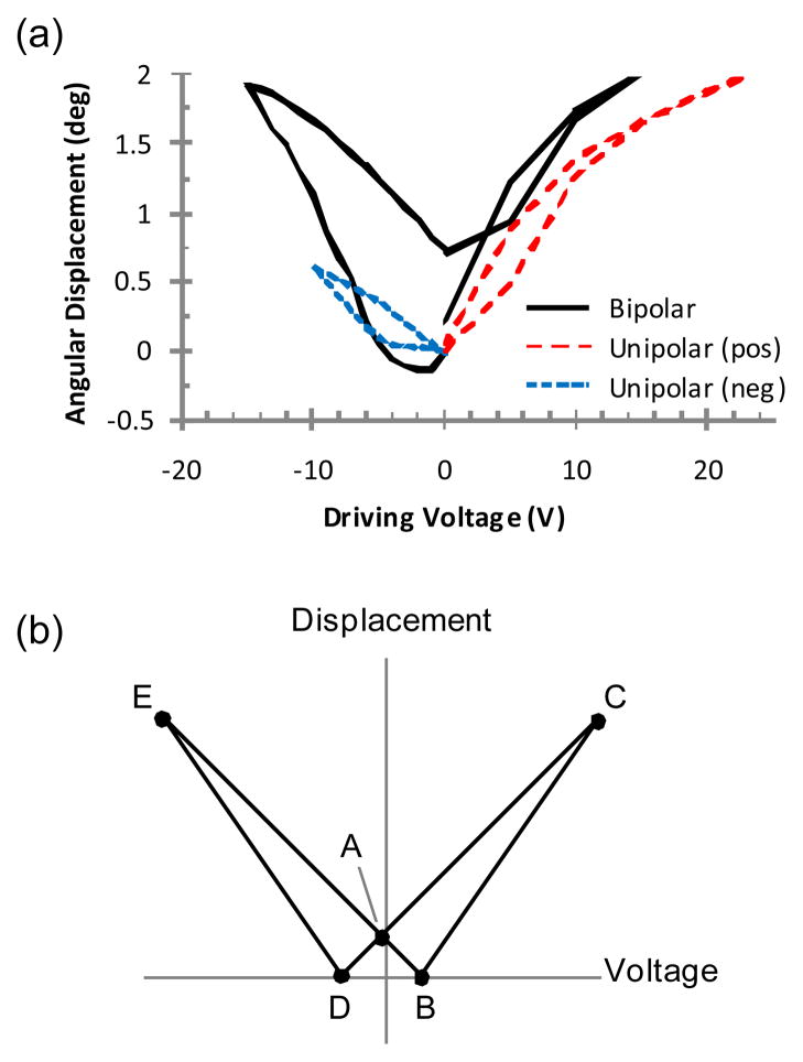
The scanning response of a stress compensated mirror device with minimal native tilt is shown in figure 5a. When driven with a bipolar voltage, there is a direction reversal near zero volts. The scanning amplitude is small. In order to utilize these mirrors in a typical scanning application, unipolar driving voltages that avoid the direction reversal can be used as shown by the dashed lines in the figure. Note that the movement is in the same direction for both voltage polarities. This displacement behavior agrees with the well known butterfly loop for piezoelectric actuators which indicates that the displacement reverses direction at voltages equivalent to the coercive field [14]. Coercive field is the electric field required to switch the polarity of ferroelectric domains, and it corresponds to a direction reversal in electromechanical strain due to domain wall motion in a piezoelectric material. An idealized butterfly loop for piezoelectrics is illustrated in figure 5b with the coercive field indicated by points B and D, and the maximum driving voltages indicated by points C and E.
Figure 5.
(a) Angular scanning of a mirror device with minimal native tilt in response to bipolar and unipolar driving voltages. (b) Illustration of typical butterfly displacement in piezoelectric cantilevers. Point A is the initial position with zero applied field. Points B and D correspond to the coercive field, and C and E are the maximum applied voltages.
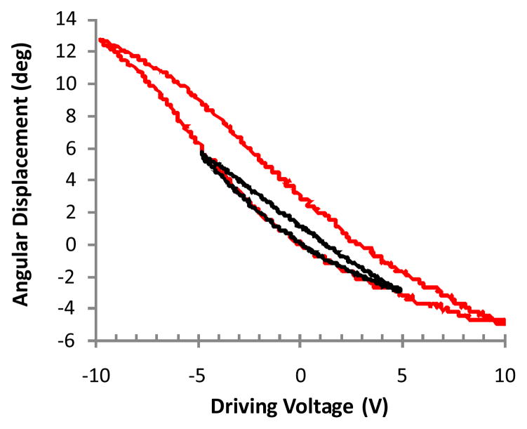
The response of a mirror with a large upward native tilt (α0 = +45°) to a bipolar driving voltage is shown in figure 6. Mechanical angular displacement is relative to the native tilt. This mirror responds very differently than the flat cantilever device of figure 5 with a much larger scanning range (17° instead of 2° for 20Vpp) and no direction reversal. When the top electrode is biased positively with respect to the bottom electrode, the mirror tilts downward relative to the starting position. Reversing the bias results in an upward tilt.
Figure 6.
Angular displacement for a mirror device with large upward native tilt driven with10Vpp and 20Vpp triangular waves. The cantilever length is 500 μm and the PZT thickness is 0.64 μm.
The angular displacement curve reported in figure 6 differs from what has been reported in the literature for thin film piezoelectric actuators, which show the butterfly response of figure 5b. Smits et al. reported a MEMS mirror actuated by thin film PZT deposited on two silicon beams that exhibited butterfly displacement behavior [13]. Similar displacement curves with direction reversal were reported by Kobayashi et al. for silicon microcantilevers actuated with PZT [19] and with LNO buffered PZT[20]. The devices reported in this paper differ because the cantilevers are completely released from the substrate without retaining any of the underlying silicon, the overall cantilever stack is much thinner, and a stress balancing layer is present on the top of the cantilever. Numerous devices with upward native tilt were tested and none exhibited reversal of the displacement direction at the coercive field. To ensure that displacement reversal was not occurring beyond the driving voltage limitation of the automated measurement system, displacement data was manually acquired at voltages up to +40 and −40 V for one device with 0.96 μm thick PZT film and 300 μm long cantilever. The displacement curve became nearly flat at extreme negative voltage and there was slight displacement reversal at +35 V, but no true butterfly behavior.
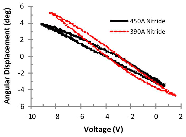
In order to further validate the relationship between the native tilt and the scan range, we analyzed two devices from the same wafer, but deposited an additional 60 A of silicon nitride to one of the devices. The additional silicon nitride reduced the native tilt α0 from greater than 45° to 22°, and decreased the scanning range as shown by the solid curves of figure 7. These results suggest that the stress balance of the cantilever to produce a flat native profile has a significant impact on device performance. A small increase in the thickness of the top layer of silicon nitride reduced the native tilt in half and reduced the linear scan range by 30%. The silicon nitride film is present in all of the devices, so this result is not related to differences in film interfaces, and the overall thickness difference is not significant enough to explain the large performance disparity. Further characterization of the PZT film and a theory for the observed electromechanical behavior is presented in section 3.3.
Figure 7.
(a) Angular displacement with 10 Vpp driving voltage for two devices with identical structure (1600 × 840 μm mirror with 500 μm long cantilever, 0.64 μm PZT) other than the thickness of silicon nitride stress balance layer. The increased silicon nitride thickness reduced the native tilt from >45° to 22°.
3.2 Optimization of drive voltage
A series of measurements was performed to optimize the driving voltages for large-range scanning applications. Because the devices with large upward tilt provided larger scanning range, we concentrated on evaluating these devices. The longer the cantilever the larger the displacement, but a small footprint actuator is desirable for endoscopic applications. We evaluated how much angular motion can be gained by increasing the applied voltage. The maximum field allowable in a bulk piezoelectric is 10–20 kV/cm [21], but values of +/− 300 kV/cm are reported for thin films [22]. Voltages exceeding 600 kV/cm have been applied to the PZT films used in this work without evidence of breakdown.
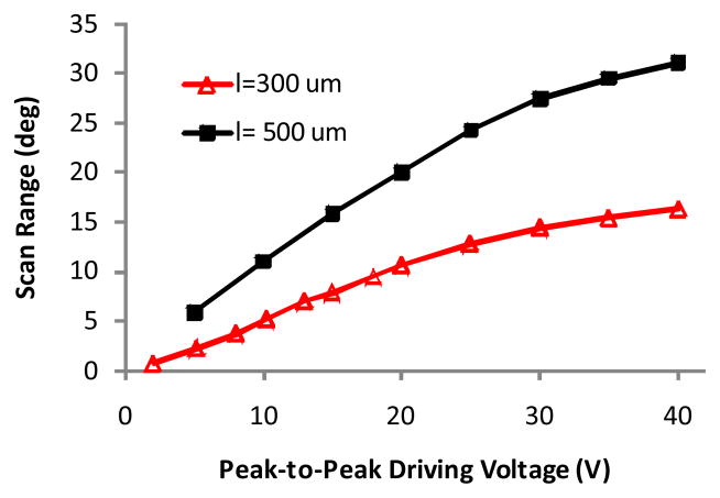
Increasing the driving voltage increases the angular scan range linearly for peak-to-peak voltage amplitudes up to 20V and then begins to level off as shown in figure 8 as drive voltage exceeds the coercive field level and polarization saturation begins to occur. The angular scan range is defined as the difference between maximum and minimum angle values at each driving voltage. Overall scan range of greater than 30° (mechanical angle) was achieved in these devices with 500μm long cantilevers, which is a significantly larger range than reported in the literature for piezoelectric cantilever scanning mirrors with longer cantilevers [13, 14] [23].
Figure 8.
Plot of total mechanical angle scan range (difference between maximum and minimum angular position) as a function of driving voltage for two devices with actuator lengths of 300 μm and 500 μm.
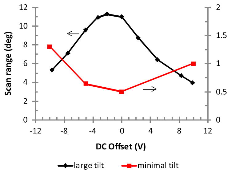
The impact of adding a dc offset to the driving waveform was investigated by measuring the total angular scan range with a 10 Vpp driving waveform for different offset values. Figure 9 provides the compiled scan range results for a mirror with large native tilt and mirror with minimal native tilt. For all upward tilted mirrors, optimal displacement performance was obtained with zero or slightly negative bias. Interestingly, this is the opposite response to behavior reported in an investigation explicitly analyzing the effect of DC bias on piezoelectric actuation [19]. In that work, little displacement was observed at zero offset, whereas the actuator performance improved rather symmetrically with both positive and negative offset. Similar behavior was observed for flat, stress-compensated mirrors as shown in figure 9. Recall that the flat mirrors also displayed typical butterfly displacement behavior as did the mirrors used for the investigations in [19].
Figure 9.
Plot of total scan range with 10 Vpp driving voltage for different dc offsets for a device with large native tilt (500 μm long cantilever) and a device with minimal native tilt (400 μm long cantilever). Note that a different scale (0 to 2°) is used for the minimal native tilt (stress-balanced) mirror due to the small scan range.
3.3 Theoretical considerations and PZT film properties
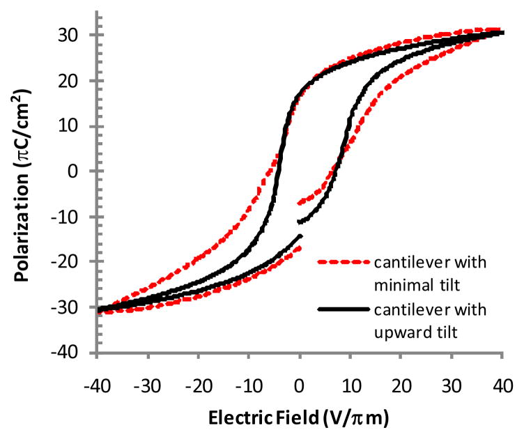
Ferroelectric polarization loops were measured for both large upward tilted and minimally tilted devices, and no large differences in coercive fields or polarization levels were observed as shown in figure 10. The coercive fields differ by less than 10%, whereas the scanning ranges differ by an order of magnitude. Slightly greater hysteresis was observed in the cantilever with minimal tilt indicating more difficulty in ferroelectric domain switching.
Figure 10.
Ferroelectric polarization loops comparing a device with large native tilt to one with minimal native tilt. The minimally tilted cantilever was 200 μm long with 1μm thick PZT. The upward tilted cantilever was 300 μm long with 0.96 μm thick PZT.
In order to understand the very different electromechanical behavior observed in devices with similar ferroelectric polarization characteristics, the mechanisms for generating movement in the PZT films were evaluated using models for ferroelectric domain behavior reported in the literature [24–26]. In the ferroelectric phase for compositions near the morphotropic phase boundary (i.e. PZT 52/48), PZT contains a mix of tetragonal and rhombohedral unit cells with spontaneous polarization in the direction of the long axis (e.g., c-axis for tetragonal unit cells). In both single crystal ferroelectric materials and ferroelectric polycrystalline thin films, the polarization is not uniformly aligned but distributed in domains separated by domain walls. C-aligned domains contain unit cells with the long axes oriented parallel to the applied field, and a-aligned domains contain unit cells with the short axes parallel to the applied field. The initial arrangement of the domains in thin film piezoelectrics is influenced by the mechanical stress in the film.
Application of an electric field to a ferroelectric material reorients polarization domains and the walls between them. As the electric field increases, domains with an unfavorable direction of polarization will start to switch so that their long axes better align with the applied field. Intrinsic contributions are those that originate from single domains, whereas extrinsic responses are mainly due to domain wall motion. Extrinsic 180° switching is a reversible process that does not contribute to piezoelectric strain. Extrinsic non-180° switching is an irreversible process that involves reorientation between a-axis alignment and c-axis alignment, and the domains remain in the switched state after the electric field is removed. This mechanism contributes to piezoelectric strain but is not typically observed in clamped piezoelectric films [25]. Extrinsic contributions that are responsible for up to 75% of piezoelectric activity in bulk material are dampened in films with substrate-induced domain clamping [25, 26]. We theorize that the stress-balanced cantilevers exhibit much less displacement and greater degree of domain clamping in the PZT film compared to cantilevers with large native tilt.
A dielectric permittivity measurement technique [25] was used to determine the degree of irreversible non-180° domain switching in both curled (large native tilt) and flat (stress-balanced) cantilevers as compared to a PZT film deposited on bulk silicon. Because a-axis aligned domains have a higher dielectric constant (K) than c-axis aligned domains when measured in the thickness direction, the capacitance value reflects the degree of a-domain alignment in the direction of the measuring field. The capacitance can be measured as a function of applied dc bias to determine the degree of irreversible switching between a- and c-axis alignment. For example, a decrease in capacitance with increasing dc bias indicates switching from a to c domain orientation in the thickness or field direction.
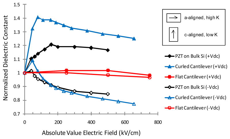
PZT films in this work were measured by applying dc bias to the film for 1 min and then removing prior to the capacitance measurement. Therefore, only irreversible switching was reflected in the measurement. Prior to the initial capacitance measurement, films were pre-poled at 500 kV/cm with voltage of opposite polarity (e.g. −Vdc pre-poling for capacitance measurement with +Vdc applied) so that the dc bias applied prior to capacitance measurement induced domain switching behavior. After pre-poling, capacitance was measured at 1 Vac, 1 kHz after increments of increasing dc bias were applied. Figure 11 shows the normalized dielectric constants obtained from the capacitance data for both positive and negative dc bias. For positive dc bias, the curled cantilever shows the greatest degree of irreversible domain reorientation. After application of a positive dc bias, the capacitance sharply increased indicating increased a-domain alignment. The capacitance of the flat cantilever was nearly constant indicating extreme domain clamping. The flat cantilever appeared to be even more clamped than a PZT film on bulk silicon. For negative dc bias, the curled cantilever behaved more similarly to the PZT on bulk silicon with the exception of the spike in a-domain alignment at low dc bias.
Figure 11.
Normalized dielectric constant plotted as a function of positive or negative dc field (+Vdc or −Vdc). Measurements were taken after the field was removed to indicate only irreversible domain switching. Inset illustrates the relationship to domain orientation, with arrows indicating direction of long-axis (i.e. c-axis) polarization in the unit cell for the two domain orientations.
This behavior can be better understood by considering the film stresses. In all three cases, tensile PZT films were deposited on a substrate with a compressive thermal oxide layer under the bottom electrode. When a non-stress-balanced (i.e., large native tilt) cantilever is released from the silicon substrate by DRIE, the oxide layer is allowed to expand and the PZT layer is allowed to contract resulting in upward curling of the stack which lowers the tensile stress in the PZT. Therefore, the PZT is less clamped by tensile stress compared to the PZT film on bulk silicon case. For the case of a stress-balanced (i.e., flat) cantilever, the upward curl is prohibited by a compressive layer deposited on top of the PZT. When the cantilever is released from the substrate, expansion of the bottom thermal oxide layer is enabled; however, the flat profile is maintained by the stress-balancing oxide layer. The PZT is therefore forced into even greater tensile stress than a film on bulk silicon producing extreme domain clamping.
The varying degree of domain clamping can explain the large discrepancy in displacement behavior for the curled and flat cantilevers. For a flat, stress-balanced cantilever, domain clamping prevents extrinsic contribution to the piezoelectric response, so the overall displacement amplitude is small and butterfly displacement behavior typical of intrinsic piezoelectric response is observed. The response of these cantilevers is limited by intrinsic contributions only. For cantilevers with large native tilt, much higher displacement amplitude is observed due to the lesser degree of domain clamping and increased extrinsic contribution to the piezoelectric response. The non-butterfly shaped displacement behavior for these cantilevers can be ascribed to the internal film stress in the PZT layer which produces asymmetry in the domain switching behavior depending on polarity of the voltage applied. Such behavior has been observed in stress-biased unimorph bulk ceramic actuators where domain switching was more favorable for positive voltage polarity due to internal stress in the piezoelectric layer, producing asymmetric displacement characteristics and delaying displacement reversal to higher applied field levels [27]. Asymmetric behavior is apparent for cantilevers with large upward tilt which exhibit larger displacement amplitude due to extrinsic contributions but no butterfly displacement characteristics as shown in figure 6. Extrinsic mechanisms are more significant for positive angular displacements which correspond to increased upward curl of the cantilever. This upward curling is a more favored position because it lessens the tensile stress in the PZT layer. On the contrary, negative angular displacements correspond to an increase in tensile stress and therefore an increase in domain clamping and decrease in displacement amplitude.
3.4 Evaluation of Calculated Displacement
Angular displacement was estimated from the equation derived by Smits et al [13] using a simplified version of the cantilever consisting of a piezoelectric layer over a substrate film with geometrical parameters length (l), width (b), substrate thickness (tsub) and PZT thickness (tPZT). Upon voltage application, the piezoelectric strain produces a tip displacement (y) approximated by (1):
| (1) |
where A = Esub/EPZT, B = tsub/tPZT, D = A2B4+2A(2B+3B2+2B3)+1.
The angular displacement α is calculated from the tip displacement as arctan(y/l) and using tabulated materials parameters for the Young’s modulus (E) (EPZT = 7×10¹⁰ Pa, Esub = 7.5×10¹⁰ Pa) and the piezoelectric constant (d31 = 0.85×10⁻¹⁰ m/V [13]).
Experimentally, we observed for a PZT cantilever integrated with a MEMS mirror a linear increase in displacement with the cantilever length, as expected. The equation predicts increased displacement for thinner PZT and this motivated us to investigate two thicknesses. The experimental values for the mirror with large native tilt were surprisingly similar to each other for both of the PZT thicknesses investigated (0.64 μm and 0.96 μm) and agreed with the calculated displacement for 0.96 μm thick PZT. For a 500 μm long cantilever with 10 Vpp applied, the equation predicts 9.3° and 16.0° scanning ranges for 0.96 and 0.64 μm PZT thicknesses respectively. The average measured scanning ranges were 10.2° for 0.96 μm PZT and 9.1° for the 0.64 μm PZT. It has been shown that thinner PZT films have reduced piezoelectric response compared to thicker films due to domain pinning effects [25]. This is likely the reason for the lack of improvement in angular displacement in the cantilever with thinner 0.64 μm PZT. The model did not accurately predict the behavior of the flat, stress-balanced cantilever devices which had a much lower scan range than calculated. The equation is based solely on bulk piezoelectric coefficients which are reduced for films with stress-clamped domains. Calculation of piezoelectric coefficients for films with different stress states is beyond the scope of this work.
3.5 Dynamic response characterization
Resonance frequency was measured by driving the mirrors with a 4Vpp sinusoidal voltage with increasing frequency while monitoring displacement with the position sensitive detector. Figure 12 shows the frequency response of three different devices with large native tilt. The resonance frequency decreased from 520 Hz to 350 Hz when the cantilever increased in length from 300 μm to 500 μm. These values are in reasonable agreement with estimates from equation f= 1/2π √(k/m), with where k = bt3E/4l3 is the spring constant of the cantilever and m is the mass of the mirror located in the center of the mirror. Because the resonance frequency does not depend on the piezoelectric properties of the cantilever, agreement with calculated values was not complicated by the cantilever stress state. The size of the mirror does not affect the resonance frequency in the data shown because the cantilever width was equal to the mirror width. The larger cantilever width cancels out larger mass in the calculation, and the experimental data is in agreement. Devices with longer cantilevers have broader resonance peaks, but this is not significant for sub-resonance operation.
The lower resonance frequency of the longer cantilever reduces their ability to follow triangular driving voltages at low frequency. While the 300 μm cantilevers can follow an arbitrary 10 Hz waveform, the 500 μm cantilever exhibits ripples at 10 Hz. Because operation in stop and hold mode may be desirable, we also characterized devices in response to a square wave. Settling time following the voltage switch is 75–100 ms for the 300 μm cantilever.
Hysteresis can be a limitation in the application of piezoelectric devices as actuators. Significant hysteresis requires electrical compensation in the drive signal or removal of the retrace signal from the image acquisition. Hysteresis is reduced when the driving voltage is unipolar and the polarization of the PZT material does not change sign. However with unipolar driving voltage, the total angular scan range is reduced, as the steeper slope in angular displacement which occurs around zero volts as shown in figure 6 is not exploited. Hysteresis is also dependent on scanning speed as shown in figure 12(b). Hysteresis measured as the position difference at the center of the scan (−4V) doubles going from 1Hz to 10Hz and quadruples at 100 Hz. The data suggest that for low speed scans, hysteresis may be small enough using unipolar drive to enable uncompensated operation.
4. Conclusion
There is a large parameter space for piezoelectrically actuated mirrors which includes numerous tradeoffs between footprint, scanning range, scanning speed, hysteresis, and linearity. The smallest footprint actuators we demonstrated have 300 μm long cantilever devices and achieved a 10° mechanical scan range at +/−10V with good linearity and resonance frequencies greater than 500 Hz. Devices with 500 μm long cantilevers achieved a 30° mechanical scan range at +/−20V with resonance frequencies greater than 300 Hz. This angular scan range is greater than reported values for other piezoelectric scanning mirrors of similar dimension and we attribute this improvement to the thin actuator arm compared to the thicker mirror segment and the high piezoelectric activity of the PZT film.
The stress balancing of cantilever curvature has a large impact on scanning performance. Stress-balanced cantilevers with a flat native profile have a small scan range due to clamping of the ferroelectric domains. Domain clamping was evident through permittivity measurements indicating minimal extrinsic domain wall contribution as well as larger hysteresis in the ferroelectric polarization behavior indicating more difficulty in domain switching. Cantilevers with large native curl have large scanning range due to large extrinsic contributions in the piezoelectric response and reduced tensile stress in the PZT layer.
The dynamic response of the devices was characterized. With resonance frequencies on the order of hundreds of Hz and a flat response in subresonance regime, the piezomirrors have adequate dynamic response for high speed imaging techniques such as OCT as well as the flexibility to operate at slower speeds for image modalities benefiting from long integration times.
Highlights.
We demonstrate piezoelectric scanning mirrors with a mechanical scan range as high as 30 degrees for a compact 500 um long actuation cantilever.
We investigate device displacement and speed as a function of fabrication and operational parameters.
Film stress balance of the actuation cantilever has a significant impact on device electromechanical performance.
Piezoelectric film properties are reported to support the proposed relationship between scanning range and cantilever stress balance.
Acknowledgments
This project was partially supported by National Institute of Health –NIBIB (1R21EB007757-01).
Footnotes
Publisher's Disclaimer: This is a PDF file of an unedited manuscript that has been accepted for publication. As a service to our customers we are providing this early version of the manuscript. The manuscript will undergo copyediting, typesetting, and review of the resulting proof before it is published in its final citable form. Please note that during the production process errors may be discovered which could affect the content, and all legal disclaimers that apply to the journal pertain.
References
- 1.Wilson BC. Detection and treatment of dysplasia in Barrett’s esophagus: a pivotal challange in translating biophotonics from bench to bedside. Journal of Biomedical Optics. 2007;12:051401. doi: 10.1117/1.2795688. [DOI] [PubMed] [Google Scholar]
- 2.Anandasabapathy S. Endoscopic imaging: emerging optical techniques for the detection of colorectal neoplasia. Current Opinion in Gastroenterology. 2008;24:64–69. doi: 10.1097/MOG.0b013e3282f2df8d. [DOI] [PubMed] [Google Scholar]
- 3.Ra HR, Piyawattanametha W, Taguchi Y, Lee D, Mandella MJ, Solgaard O. Two-Dimensional MEMS Scanner for Dual-Axes Confocal Microscopy. Journal of Microelectromechanical systems. 2007;16:969–976. [Google Scholar]
- 4.Jung W, Tang S, McCormick DT, Xie T, Ahn Y-C, Su J, Tomov IV, Krasieva TB, Tromberg BJ, Chen Z. Miniaturized probe based on a microelectromechanical system mirror for multiphoton microscopy. Optics Letters. 2008;33:1324–1326. doi: 10.1364/ol.33.001324. [DOI] [PMC free article] [PubMed] [Google Scholar]
- 5.Wang Z, Lee CSD, Waltzer WC, Liu J, Xie H, Yuan Z, Pan Y. In vivo bladder imaging with microelectromechanical-systems-based endoscopic spectral domain optical coherence tomography. Journal of Biomedical Optics. 2007;12:034009. doi: 10.1117/1.2749744. [DOI] [PubMed] [Google Scholar]
- 6.Myaing MT, MacDonald DJ, Li X. Fiber-optic scanning two-photon fluorescence endoscope. Optics Letters. 2006;31:1076–1078. doi: 10.1364/ol.31.001076. [DOI] [PubMed] [Google Scholar]
- 7.Huo L, Xi J, Wu Y, Li X. Forward-viewing resonant fiber-optic scanning endoscope of appropriate scanning speed for 3D OCT imaging. Opt Express. 2010;18:14375–14384. doi: 10.1364/OE.18.014375. [DOI] [PMC free article] [PubMed] [Google Scholar]
- 8.Kumar K, Condit JC, McElroy A, Kemp NJ, Hoshino K, Milner TE, Zhang X. Fast 3D in vivo swept-source optical coherence tomography using a two-axis MEMS scanning micromirror. J Opt A: Pure Appl Opt. 2008;10:044013. [Google Scholar]
- 9.Wu L, Xie H. Electrothermal micromirror with dual-reflective surfaces for circumferential scanning endoscopic imaging. J Micro/Nanolith MEMS MOEMS. 2009;8:013030. [Google Scholar]
- 10.Jia K, Pal S, Xie H. An electrothermal tip-tilt-piston micromirror based on folded dual s-shaped bimorphs. Journal of Microelectromechanical systems. 2009;18:1004–1014. [Google Scholar]
- 11.Wu L, Xie H. A large vertical displacement electrothermal bimorph microactuator with very small lateral shift. Sensors and Actuators A. 2008;145–146:371–379. [Google Scholar]
- 12.Gilchrist KH, McNabb RP, Izatt JA, Grego S. Piezoelectric scanning mirrors for endoscopic optical coherence tomography. J Micromech Microeng. 2009;19:095012. [Google Scholar]
- 13.Smits JG, Fujimoto K, Kleptsyn VF. Microelectromechanical Flexure PZT Actuated Optical Scanner: Static and Resonance behavior. Journal of Micromechanics and Microengineering. 2005;15:1285–1293. [Google Scholar]
- 14.Kobayashi T, Tsaur J, Maeda R. Fabrication of Optical Microscanners Driven by PZT Actuators. Japanese Journal of Applied Physics. 2005;44:7078–7082. [Google Scholar]
- 15.Koh KH, Kobayashi T, Hsiao F-L, Lee C. Characterization of piezoelectric PZT beam actuators for driving 2D scanning micromirrors. Sensors and Actuators A: Physical. 2010;162:336–347. [Google Scholar]
- 16.Koh KH, Kobayashi T, Xie J, Yu A, Lee C. Novel piezoelectric actuation mechanism for a gimbal-less mirror in 2D raster scanning applications. J Micromech Microeng. 2011;21:075001. [Google Scholar]
- 17.Haertling GH. An acetate precursor process for bulk and thin film PLZT. Proc IEEE 7th Int Symp Applied Ferroelectrics. 1990:292–295. [Google Scholar]
- 18.Jain A, Kopa A, PY, Fedder GK, Xie H. A two-axis electrothermal micromirror for endoscopic optical coherence tomography. IEEE Journal of Selected Topics in Quantum Electronics. 2004;10:636–642. [Google Scholar]
- 19.Kobayashi T, Maeda R, Itoh T. The influence of DC bias on the displacement and sensor output of self-sensitive piezoelectric microcantilevers. J Micromech Microeng. 2008;18:035025. [Google Scholar]
- 20.Kobayashi T, Ichiki M, Kondou R, Nakamura K, Maeda R. Fabrication of piezoelectric microcantilevers using LaNiO3 buffered Pb(Zr,Ti)O3 thin film. J Micromech Microeng. 2008;18:035007. [Google Scholar]
- 21.www.physikinstrumente.com.
- 22.Damjanovic D. Ferroelectric, dielectric and piezoelectric properties of ferroelectric thin films and ceramics. Rep Prog Phys. 1998;61:1267–1324. [Google Scholar]
- 23.Kobayashi T, Maeda R, Itoh T. Low speed piezoelectric optical microscanner actuated by piezoelectric microcantilevers using LaNiO3 buffered Pb(Zr,Ti)O3 thin film. Smart Mater Struct. 2009;18:065008. [Google Scholar]
- 24.Trolier-McKinstry S, Muralt P. Thin film piezoelectrics for MEMS. J Electroceram. 2004;12:7–17. [Google Scholar]
- 25.Xu F, Trolier-McKinstry S, Ren W, Baomin X, Xie ZL, Hemker KJ. Domain wall motion and its contribution to the dielectric and piezoelectric properties of lead zirconate titanate films. J Appl Phys. 2001;89:1336–1348. [Google Scholar]
- 26.Bassiri-Gharb N, Fujii I, Hong E, Trolier-McKinstry S, Taylor D, Damjanovic D. Domain wall contributions to the properties of piezoelectric films. J Electroceram. 2007;19:47–65. [Google Scholar]
- 27.Dausch DE. Asymmetric 90° domain switching in rainbow actuators Ferroelectrics. Ferroelectrics. 1998;210:31–45. [Google Scholar]


