The discovery of fullerenes (1) provided exciting insights into how architectures built from pure carbon units can result in new symmetries and structures with remarkable physical properties. Carbon nanotubes represent the most striking example (2). A carbon nanotube can be considered as the ultimate fiber, reflecting highly organized, near ideal sp2 bonded carbon structure. The organization of the hexagonal honeycomb carbon lattice into cylinders with helical arrangement of hexagonal arrays has created a very unusual macromolecular structure that is by far the most superior carbon fiber ever made.
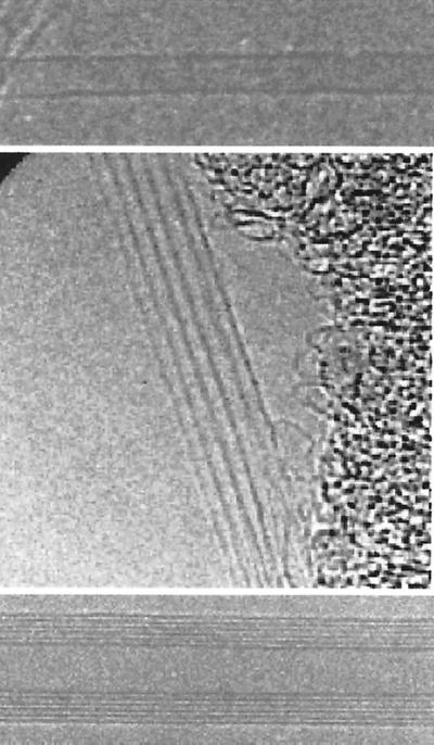
The discovery of nanotubes happened in 1991 when Dr. Sumio Iijima of NEC corporation found these tiny needles on electrodes used to prepare fullerenes (3). What he first observed were multiwalled nanotubes (MWNTs) consisting of coaxial cylindrical units (4) (Fig. 1); single-walled nanotubes (SWNTs), which often bundle up via Van der Waals forces into larger assemblies of ropes, came along a few years later (5, 6) (Fig. 1). Several methods exist today to synthesize these structures, including electric arc-discharge (4, 7), laser ablation (8), and catalytic chemical vapor deposition (9). In all of these, carbon vapor is made to condense into tubular structures, with or without the presence of catalysts, which are mostly nanoparticles of transition metals. The diameter of SWNTs range narrowly between 1 and 2 nm and that of MWNTs are 2–25 nm. They both run microns in length, providing large aspect ratios.
Figure 1.
Transmission electron microscopy images showing a SWNT (Top), organized SWNT bundle (Middle), and a MWNT (Bottom). Isolated SWNT is ≈1.4 nm, the bundle is ≈6 nm, and the MWNT is ≈8 nm in diameter.
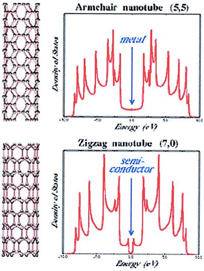
The nanotube structure and topology can be characterized by two integer numbers (n, m), which define the peculiar symmetries of Armchair and Zigzag (Fig. 2) and helical classes of nanotube structures. After the discovery, theoretical works (10–13) predicted that the electronic properties of nanotubes depend on their helicity and diameter. The general rule is that the tubes exhibit metallic or semiconducting behavior, depending on (n, m). Very recently, using scanning tunneling microscope probes (14, 15), experimentalists have measured the density of electronic states (DOS), tube diameter, and helicity simultaneously, confirming theoretical predictions. In addition, sharp peaks in the DOS are observed, which are the characteristic signatures of the one-dimensional (1D) nature of conduction within a 1D system. The 1D nature of the electron system in nanotubes has been observed by resonant Raman scattering experiments (16).
Figure 2.
Electronic properties of two different carbon nanotubes. The Armchair (5,5) nanotube (Upper) exhibits a metallic behavior (finite value of charge carriers in the DOS at the Fermi energy). The Zigzag (7,0) nanotube (Lower) is a small gap semiconductor (no charge carriers in the DOS at the Fermi energy). Sharp spikes in the DOS are Van Hove singularities.
Because of their intrinsic structural robustness, high electrical conductivity (with current carrying capacity of 109 amp/cm2) and high aspect, nanotubes show great promise for applications. Studies of field emission from MWNTs have demonstrated large currents at low operating voltages (17). Nanotubes emit coherently, indicating possible use in electron holography. Electron emission from arrays of tubes have been used to construct an actual device: a cathode ray tube lighting element. Nanotube arrays now can be grown on glass substrates for field-emitting flat panel displays.
Techniques for the robust attachment of MWNTs to the ends of atomic force microscope (AFM) cantilevers have been developed for their use as scanning probe tips (18). Such tips have a number of advantages, including crash-proof operation and the capability of imaging deep structures inaccessible to conventional tips. Such tips have been used as high-resolution probes in electrostatic force microscopy and in nanolithography for writing 10-nm wide lines at relatively high speeds. Making use of the fact that chemistry can be restricted to the ends of the nanotubes (where topological defects are present) the AFM nanotube tip can be functionalized with distinct chemical groups (19) and used to demonstrate nanoscale imaging with the ability to discriminate local chemistry of the surface being probed.
The development of nanoelectronics based on nanotubes is certainly a most promising direction in nanotechnology. With SWNTs, physicists have found a 1D carbon-based molecule that can conduct electricity at room temperature with essentially no resistance. This phenomenon is known as ballistic transport, where the electrons can be considered as moving freely through the structure, without any scattering from atoms or defects. Electrical conduction in finite-sized SWNTs occurs through well-separated, discrete electron states that are quantum-mechanically coherent over long distances (≈3 μm), with electron wave functions extending over the entire tube (20). Semiconductor nanotubes connected to two metal electrodes can be made to function as field-effect nanotransistor. By applying a voltage to a gate electrode, the nanotube can be switched from a conducting to an insulating state at room temperature (21). Such nanodevice fabrication represents an important step toward implementing molecular electronics. Other device applications have been investigated theoretically. Joining a semiconducting nanotube to a metallic one, using pentagon-heptagon pair incorporated in the hexagonal network, has been proposed as the basis of a nanosize diode (22).
The as-produced nanotubes, which are generally too long and tangled for convenient use in electronics, now can be cut into submicron length sections (23), sorted by length, and have their ends and side walls rationally functionalized and solubilized (24) in organic solvents. Such advances are precursor steps to the time when size and property selected nanotubes can be assembled, en masse, into functional circuits.
There is great interest in developing lightweight, high- performance polymer composites using nanotubes as fillers (25). As nanotubes can be considered as the ultimate carbon fiber, the thought is that they will one day replace existing micron-size carbon fibers in composites. The mechanical response of nanotubes is strikingly different from carbon fibers; necking occurs in nanotubes through defect migration causing changes in lattice helicity and the onset of plastic deformation occurs at large strains with superplastic behavior (26). The elastic modulus of the nanotubes have been determined indirectly (27) and is found to be the highest among known materials.
Other unique applications of nanotubes have been demonstrated. Free-standing films of purified SWNTs have shown promise for application as the anode intercalation host in lithium ion rocking chair batteries with high charging capacities. SWNT films embedded in electrolytes have been shown to be efficient electromechanical actuators (28) with possible application as artificial muscles. Such actuators have demonstrated ≈1% strains at ≈1 V that fares much better than piezoelectric actuators, which require hundreds of volts to achieve comparable strains. Nanotubes are being considered as energy storage/delivery systems because of possibilities of hydrogen storage and their excellent electron transfer characteristics (29). The concept of filling nanotubes with metallic and inorganic compounds have been used to prepare unique nanowires using nanotubes as 1D templates (30).
In summary, it is rare to come across a material that has such a range of remarkable properties. Scientists also have found a robust 1D system that provides insightful fundamental molecular behavior and new physics. The rapid progress made in developing applications for nanotubes chronicles the remarkable versatility of these structures.
Abbreviations
- MWNT
multiwalled nanotube
- SWNT
single-walled nanotube
- DOS
density of electronic states
- 1D
one-dimensional
Footnotes
This paper is a summary of a session presented at the fifth annual German-American Frontiers of Science symposium, held June 10–13, 1999, at the Alexander von Humboldt Foundation in Potsdam, Germany.
References
- 1.Kroto H W, Heath J R, O’Brien S C, Curl R F, Smalley R E. Nature (London) 1985;318:162–164. [Google Scholar]
- 2.Dresselhaus M S, Dresselhaus G, Eklund P C. Science of Fullerenes and Carbon Nanotubes. New York: Academic; 1996. [Google Scholar]
- 3.Iijima S. Nature (London) 1991;354:56–58. [Google Scholar]
- 4.Ebbesen T W, Ajayan P M. Nature (London) 1992;358:220–222. [Google Scholar]
- 5.Iijima S, Ichihashi T. Nature (London) 1993;363:603–605. [Google Scholar]
- 6.Bethune D S, Kiang C H, de Vires M S, Gorman G, Savoy R, Vazquez J, Beyers R. Nature (London) 1993;363:605–607. [Google Scholar]
- 7.Journet C, Maser W K, Bernier P, Loiseau A, Lamy de la Chappelle M, Lefrant S, Deniard P, Lee R, Fischer J E. Nature (London) 1997;388:756–758. [Google Scholar]
- 8.Thess A, Lee R, Nikolaev P, Dai H, Petit P, Robert J, Xu C, Lee Y H, Kim S G, Rinzler A G, et al. Science. 1996;273:483–487. doi: 10.1126/science.273.5274.483. [DOI] [PubMed] [Google Scholar]
- 9.Li W Z, Xie S S, Qian L X, Chang B H, Zou B S, Zhou W Y, Zhao R A, Wang G. Science. 1996;274:1701–1703. doi: 10.1126/science.274.5293.1701. [DOI] [PubMed] [Google Scholar]
- 10.Hamada N, Sawada S, Oshiyama A. Phys Rev Lett. 1992;68:1579–1581. doi: 10.1103/PhysRevLett.68.1579. [DOI] [PubMed] [Google Scholar]
- 11.Saito R, Fujita M, Dresselhaus G, Dresselhaus M S. Appl Phys Lett. 1992;60:2204–2206. [Google Scholar]
- 12.Rubio A, Corkill J L, Cohen M L. Phys Rev B. 1994;49:5081–5084. doi: 10.1103/physrevb.49.5081. [DOI] [PubMed] [Google Scholar]
- 13.Mintmire J W, Dunlap B I, White C T. Phys Rev Lett. 1992;68:631–634. doi: 10.1103/PhysRevLett.68.631. [DOI] [PubMed] [Google Scholar]
- 14.Wildoer J W G, Venema L C, Rinzler A G, Smalley R E, Dekker C. Nature (London) 1998;391:59–61. [Google Scholar]
- 15.Odom T W, Huang J L, Kim P, Lieber C M. Nature (London) 1998;391:62–64. [Google Scholar]
- 16.Rao A M, Richter E, Bandow S, Chase B, Eklund P C, Williams K A, Fang S, Subbaswamy K R, Menon M, Thess A, et al. Science. 1997;275:187–191. doi: 10.1126/science.275.5297.187. [DOI] [PubMed] [Google Scholar]
- 17.de Heer W A, Chatelain A, Ugarte D. Science. 1995;270:1179–1181. [Google Scholar]
- 18.Dai H, Hafner J H, Rinzler A G, Colbert D T, Smalley R E. Nature (London) 1996;384:147–149. [Google Scholar]
- 19.Wong S S, Joselevich E, Woolley A T, Cheung C L, Lieber C M. Nature (London) 1998;394:52–54. doi: 10.1038/27873. [DOI] [PubMed] [Google Scholar]
- 20.Tans S J, Devoret M H, Dai H, Thess A, Smalley R E, Geerligs L J, Dekker C. Nature (London) 1997;386:474–477. [Google Scholar]
- 21.Tans S J, Verschueren A R M, Dekker C. Nature (London) 1998;393:49–51. [Google Scholar]
- 22.Charlier J-C, Ebbesen T W, Lambin P. Phys Rev B. 1996;53:11108–11112. doi: 10.1103/physrevb.53.11108. [DOI] [PubMed] [Google Scholar]
- 23.Liu J, Rinzler A, Dai H, Hafner J, Bradley R, Lu A, Shelimov K, Huffman C, Rodriguez-Macias F, Boul P, et al. Science. 1998;280:1253–1255. doi: 10.1126/science.280.5367.1253. [DOI] [PubMed] [Google Scholar]
- 24.Chen J, Hamon M A, Hu H, Chen Y, Rao A M, Eklund P C, Haddon R C. Science. 1998;282:95–97. doi: 10.1126/science.282.5386.95. [DOI] [PubMed] [Google Scholar]
- 25.Schadler L S, Giannaris S C, Ajayan P M. Appl Phys Lett. 1998;73:26–27. [Google Scholar]
- 26.Yakabson B I. Appl Phys Lett. 1998;72:918–920. [Google Scholar]
- 27.Treacy M M J, Ebbesen T W, Gibson J M. Nature (London) 1996;381:678–680. [Google Scholar]
- 28.Baughman R H, Cui C, Zakhidov A A, Iqbal Z, Barisci J N, Spinks G M, Wallace G G, Mazzoldi A, DeRossi D, Rinzler A G, et al. Science. 1999;248:1340–1342. doi: 10.1126/science.284.5418.1340. [DOI] [PubMed] [Google Scholar]
- 29.Dillon A C, Jones K M, Bekkedahl T A, Kiang C H, Bethune D S, Heben M J. Nature (London) 1997;386:377–379. [Google Scholar]
- 30.Ajayan P M, Iijima S. Nature (London) 1993;361:333–334. [Google Scholar]


