Abstract
While atomic layer deposition (ALD) has been used for many years as an industrial manufacturing method for microprocessors and displays, this versatile technique is finding increased use in the emerging fields of plasmonics and nanobiotechnology. In particular, ALD coatings can modify metallic surfaces to tune their optical and plasmonic properties, to protect them against unwanted oxidation and contamination, or to create biocompatible surfaces. Furthermore, ALD is unique among thin-film deposition techniques in its ability to meet the processing demands for engineering nanoplasmonic devices, offering conformal deposition of dense and ultra-thin films on high-aspect-ratio nanostructures at temperatures below 100 °C. In this review, we present key features of ALD and describe how it could benefit future applications in plasmonics, nanosciences, and biotechnology.
I. INTRODUCTION
Atomic layer deposition (ALD) is a variant of chemical vapor deposition (CVD) techniques capable of angstrom-resolution, layer-by-layer growth of compound films.1–4 ALD can deposit these ultra-thin films in a conformal manner over a wide range of materials and high-aspect-ratio topography. It has been used extensively in commercial production, most notably for high-permittivity gate insulators in 45-nm-node silicon transistors.5,6 Beyond its adoption by the microelectronics industry, this versatile technique finds broad application in surface modification, lithographic patterning, optical tuning, layer-by-layer optical characterization, and protection and encapsulation of various nanostructures. This review focuses on these new and emerging applications, particularly in plasmonics and nanobiotechnology, and summarizes some recent research.
Overview of ALD
In a typical ALD reaction for depositing a binary compound film, the precursors “A” and “B” are sequentially introduced into a reaction chamber with an inert purging step in between: A/purge/B/purge/A/purge, etc… until the desired thickness is reached. An archetypical ALD process is the deposition of Al2O3 from trimethylaluminum (TMA) and H2O, which consists of four steps:3 (1) inject the first precursor (TMA) until its binding sites on the reaction surface are saturated; (2) purge the chamber with inert gas and remove unbound precursor; (3) inject the second precursor (H2O) and form a monolayer of hydroxyl (OH) groups on the surface; and (4) purge. Each growth step self-saturates when the surface binding sites are occupied, thus the deposited film thickness after each cycle is highly reproducible. The total film thickness can be tuned in a step-wise manner by the total number of each atomically thick ALD cycle. Importantly, the film thickness can be precisely controlled over a large area, regardless of the underlying topography, because the self-saturating growth mechanism will even out nonuniform local growth rates. Additionally, the chemical reactions in ALD occur only on surfaces, and not in the gas phase, because the precursors are injected alternately and do not mix with each other. This scheme prevents unwanted particle generation caused by gas-phase reactions, and also allows the use of highly reactive precursors such as TMA, which are difficult to use with CVD. By utilizing these highly reactive precursors, many ALD reactions can be performed at temperatures around 50–250 C, well below typical CVD temperatures. Thus ALD is an ideal method to deposit dense and conformal films on polymer, plastic, or even biological samples that cannot withstand high temperatures.
One drawback of ALD – although it may also be considered one of its key benefits – is its slow deposition rate, which is often an order of magnitude lower than the CVD rate. Usually, only a fraction of a monolayer is grown in each cycle because of steric hindrance of precursor molecules on the surface.7 Fortunately, many applications in microelectronics, and now in plasmonics, require ultra-thin (e.g. <10 nm) films, thus throughput is not a major problem. Common materials that can be deposited via ALD are Al2O3, HfO2, ZrO2, TiO2, SiO2, and some metals such as Cu, Co, Fe, Ni, and Ag.4,8,9 For comprehensive reviews on the specific chemistry of the ALD process, the reader is directed to several excellent articles.2–4,10–15
While ALD, or atomic layer epitaxy (ALE) as it was called initially, has been used for commercial production of thin-film electroluminescent flat-panel displays,2 its use has more recently marked an important milestone. Following decades of intense R&D,16 in some leading-edge microprocessors ALD-grown high-permittivity (or ‘high-k’) oxides have replaced SiO2 gate insulators, which leak very high tunneling currents below a thickness of ~10 Å.5,6 In addition, ALD can be used to make capacitors for DRAM and thin barrier layers as well as seed layers for copper interconnects.12
Besides these mature applications in the microelectronics industry, ALD has tremendous potential for nanosciences and biotechnology to coat, functionalize, or protect a diverse set of substrates such as semiconductors, glasses, oxides, metals, polymers, carbon nanotubes, or graphene. Additionally, ALD has an unmatched capability to conformally cover, encapsulate, or fill high-aspect-ratio nanostructures such as wires, gaps, pores, or deep trenches. In particular, the capability of ALD to deposit ultra-thin insulators on patterned metallic surfaces at low temperatures is essential for many applications in plasmonics and biotechnology.
II. ALD for Plasmonics
Plasmonics is a rapidly growing branch of photonics that harnesses hybrid electromagnetic waves known as surface plasmon polaritons (SPPs), which are density fluctuations of conduction electrons in metals and propagate along the metal surface like ripples on a pond. Unlike free-space light, however, SPPs are bound to the interface and decay exponentially perpendicular to the metal-dielectric interface17 and are not limited by diffraction. Indeed, it has been shown that metallic gaps, tips, apertures, wires, or particles can concentrate SPP waves to nanometric volumes, thereby enhancing light-matter interactions at unprecedented scales. The nanoscale manipulation of optical energy via SPPs can benefit a wide range of applications in sensing, imaging, spectroscopy, and lithography. Many review articles provide in-depth coverage of recent advances in plasmonics.18–23
ALD for characterization and tuning of optical nanostructures
In addition to SPPs propagating on flat or smoothly varying topographies, another important class of plasmon waves are the “localized” surface plasmons (LSP) as illustrated in Figure 1. The wave-like SPPs propagate along the metal surface and extend ~100 – 300 nm perpendicular to the metal surface for the visible frequencies. In contrast, LSPs are bound to sharp metallic tips, corners, nanoparticles, or other nanoscale patterns, and can confine optical energy more tightly with a shorter decay length of 10 – 50 nm. For both SPPs and LSPs, the maximum field intensity is at the metal surface.
Figure 1.
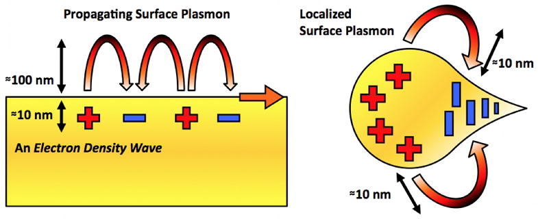
Schematics of propagating surface plasmons, known as surface plasmon polaritons (SPPs), and localized surface plasmons (LSPs). While SPPs propagate along the metal surface and decay exponentially in the perpendicular direction with a decay length of 100–300 nm in the visible frequencies, LSPs are more tightly bound on metallic nanostructures with a shorter decay length (10–50 nm).
Since SPPs are hybrid waves generated by a coupling between light and the conduction electrons, they have higher momentum than free-space light. Thus excitation of SPPs requires increasing the momentum of light by illumination of a thin metallic film through a prism in a total internal reflection mode or by grating coupling with patterned metallic surfaces.24 If the surrounding environmental refractive index changes, e.g. due to molecular binding, the excitation condition, e.g. the surface plasmon resonance (SPR) angle or wavelength, will also change. Likewise, the resonant frequency of localized surface plasmon resonance (LSPR) is also extremely sensitive to changes in surface properties such as the dielectric constants, roughness, molecular adsorption, etc. Therefore plasmons can serve as efficient probes for surface-based phenomena that are difficult to detect with other techniques based on free-space light. In fact, SPR biosensors have been successfully commercialized and used extensively in pharmaceutical research to measure molecular binding kinetics.25,26 SPR biosensors measure changes in the dielectric constant near metallic surfaces caused by molecular binding interactions. Because most proteins have refractive index values of 1.4~1.6,27,28 a thin layer adsorbed on the surface will increase the local refractive index and increase the SPR angle or wavelength.
Quantitatively, Jung et al. derived a formula to estimate the effective refractive index of a thin film, e.g. a molecular monolayer, seen by the SPP waves:29
| (1) |
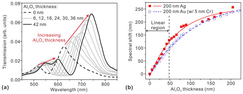
where nfilm and nmedium are the refractive indices of a thin film deposited on the metal and of the surrounding medium, respectively, and d is the thickness of the deposited film. From Eq. (1), it can be seen that neffective changes gradually from nmedium to nfilm with the increasing film thickness d. The decay length, δSP, is a function of the frequency and the geometry of the metal structure. For example, propagating SPPs have δSP around 100–300 nm in the visible regime. Since δSP is also a measure of the probing range of a given SPR sensor, any spectral shift occurs mainly for film thicknesses up to δSP, and then saturates. Because ALD can deposit conformal overlayers with a thickness resolution well below δSP, it provides a unique method to measure both the spectral response and probing range of SPR sensors. Such layer-by-layer spectral characterization, up to hundreds of nanometers in thickness, cannot be performed with real biomolecules. ALD-grown Al2O3 films have been used for distance-dependent studies of nanoparticle-based LSPR sensors30 and nanohole-based SPR sensors.31 Like metallic nanoparticles, the inverse structure, i.e. nanohole arrays in metallic films can also be used for biosensing based on the extraordinary optical transmission effect.32–40 Light transmitted through metallic nanoholes has a characteristic spectrum based on the hole size, hole periodicity, and other geometrical parameters. Molecules binding to the nanohole film cause the transmission spectrum to shift. This is due to a change in the local refractive index, as with conventional SPR sensors. As shown in Figure 2, the probing ranges of SPPs in metallic nanohole arrays can be determined from their spectral response to Al2O3 overlayers.
Figure 2.
(a) Sequence of transmission spectra through a nanohole-based SPR sensor as the thickness of ALD grown Al2O3 overlayer increases from 0 to 42 nm in a step of 6 nm. (b) The spectral response of Au and Ag nanohole-based SPR sensors as the thickness of Al2O3 overlayer deposited on the surface increases. Both nanohole SPR sensors show a linear response to the 31 thickness increases of Al2O3 layer up to 48 nm. Adapted from Im et al.
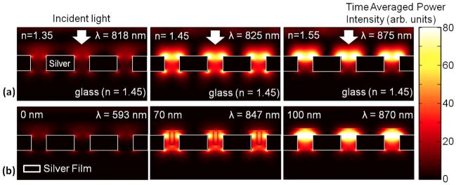
Because neffective seen by the evanescent wave changes from nmedium (e.g. air or water) to nfilm as a function of the film thickness, ALD coatings can also be used for precise spectral tuning. Yang et al. showed digital tuning of photonic crystal devices,41 and Qian et al. used ALD-grown titania shells to tune the LSPR peaks of Au nanoparticles.42 Experiments and three-dimensional computer simulations (Figure 3) have shown that successively thicker ALD overlayers can be used to boost the optical transmission through an array of metallic nanoholes by matching the effective refractive index of the top surface with that of the glass substrate.31
Figure 3.
(a) 3-D finite-difference time-domain (FDTD) computer simulations showing the time-averaged SP field intensity for different bulk refractive indices changing from 1.35 to 1.55. The maximum transmission occurs when the bulk refractive index matches with that of the glass substrate, 1.45. (b) An ALD overlayer can be also used to match the effective refractive index of the top surface with that of the glass substrate to boost the optical transmission through a metallic nanohole array. Adapted from Im et al.31
Metallic structures have also been widely used in surface-enhanced Raman spectroscopy.43 Raman spectroscopy is a powerful method for the detection of molecules by their signature vibrational (Raman) spectra. Raman spectral intensity is enhanced when molecules are within a few nanometers of a roughened metal surface, a process known as surface enhanced Raman spectroscopy or SERS. Because of the strong electromagnetic fields around metallic nanostructures, electromagnetic enhancement is the largest contributor to the surface enhancement effect. Because the electromagnetic field of the illuminated plasmonic nanostructures decays exponentially with distance, the enhancement of Raman scattering sharply changes with the distance between proximate molecules and the metal surface. Dieringer et al. used an ALD-grown Al2O3 film as a spacer to map the SERS signal intensity as the distance between the analyte molecule and the Ag surface increased. Their results showed that the Raman signal intensity decreased ten-fold for every 2.8 nm increase in the Al2O3 film thickness.44 However, because ALD alumina films can be grown with ~1 nm thicknesses, they can still act as a buffer layer to attach molecules without sacrificing the surface enhanced Raman signal intensity.
ALD for protecting metallic nanostructures
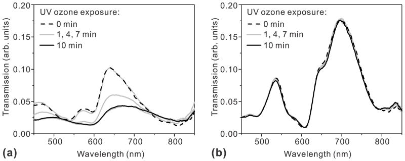
ALD-grown films can also act as a robust protection layer for metallic nanostructures. Au and Ag have been commonly employed to build plasmonic devices operating in the visible or infrared regime. At wavelengths below ~600 nm, however, Ag exhibits lower ohmic losses and lower SP damping than Au. Also, Ag is much less expensive than Au. Despite these advantages, Ag has poor chemical stability and is readily oxidized in the air. Therefore, many plasmonic devices, including the commercial Biacore ™ SPR sensor chips, are made with Au. Fortunately, the chemical stability of Ag surfaces can be improved by adding a protective layer. For plasmonic applications, the protective layer should be much thinner than δSP, i.e. below 10~20 nm, otherwise the evanescent SP field will be buried in that layer. For such an ultra-thin film to function as a barrier, it must be very dense, pinhole-free, and entirely encapsulate the patterned metals with excellent step coverage. Furthermore, the film should be deposited at a low temperature to avoid degrading or oxidizing the underlying Ag film during a deposition process. ALD can meet all of these stringent requirements, unlike CVD or physical vapor deposition (PVD). Among various materials options, Al2O3 has been widely investigated as a gas diffusion barrier.45 Al2O3 film has a high phase-transition temperature of ~800 °C and can improve the thermal stability of the underlying Ag films, while blocking the diffusion of O2 and H2O. A low-temperature ALD process at 58°C to coat poly(ethylene terephthalate) (PET) bottles with 360 Å of Al2O3 was shown to reduce CO2 gas diffusion rates compared with uncoated PET bottles.46 In other examples, Al2O3 was used to encapsulate and prevent oxidation of organic light emitting devices (OLEDs). In the context of plasmonics, groups have used Al2O3 to improve the thermal and chemical stability of Ag-based nanostructures.31, 47–49 Whitney et al. showed that Ag nanoparticles coated with a sub-1 nm thick Al2O3 capping layer can preserve plasmon resonance peaks even after annealing at 500 °C, while the same structure without ALD coating showed degraded peaks after annealing at only 200 °C.47 Likewise, Al2O3-coated Ag nanoparticles showed improved stability against local heating induced by a high-power femtosecond laser.48 In terms of chemical stability, it has been shown that Al2O3 overlayers can protect Ag-based SERS substrates with no appreciable decline in performance after 9 months of storage in ambient conditions. This suggests that ALD coated Ag substrates may be suitable for long-term deployment and field-portable applications.50 Al2O3 was also shown to protect Ag films against UV-ozone processing, which is often used before bonding oxide surfaces with polydimethylxilosane (PDMS) for microfluidics,31 as shown in Figure 4. While most existing work focused on Al2O3, other ALD-grown dielectric films such as HfO2 or ZrO2 could also be useful in the future.
Figure 4.
Transmission spectra change as nanohole arrays made in Ag lms are exposed to UV ozone for 1, 4, 7, and 10 min (a) without a protective Al2O3 overlayer and (b) with a 20 nm-thick Al2O3 overlayer. The transmission through the Ag nanohole array without the Al2O3 layer rapidly degrades during the UV ozone process while the Al2O3 coated Ag nanohole array maintains its transmission spectrum for 10 min UV ozone process. Adapted from Im et al.31
ALD and surface roughness
Because SP waves are tightly bound to the surface, roughness of even a few nanometers can cause backscattering or radiative damping of SPP waves.24 This problem is compounded since most metal films deposited by evaporation or sputtering are polycrystalline and exhibit rough top surfaces. Patterning these metals films with a focused ion beam (FIB) or other methods may roughen the surface even further. To address this challenge, template stripping has been used to produce ultra-smooth patterned metals.51 It was shown that the propagation of SPP waves in Ag films increase 3 to 7 times by reducing the roughness below 1 nm. After template stripping, however, the pristine and ultra-smooth metallic surfaces are immediately exposed to a contaminating environment. Template-stripped metal films could be capped with an ALD-grown layer without increasing the surface roughness and protect the smooth metal surface from unwanted contamination or oxidation.52 Indeed, the surface roughness of Al2O3 films after many repeated ALD cycles has been shown to be virtually indistinguishable from that of an underlying silicon substrate.53
ALD for lithographic patterning
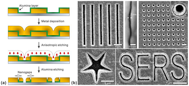
ALD can also be used in top-down lithographic patterning of metallic nanostructures. Many plasmonic devices harness ultra-thin metallic gap structures to squeeze electromagnetic energy for SERS and nonlinear optics.54 For example, single-molecule Raman spectroscopy has been demonstrated when a Raman-active molecule is positioned within the large electromagnetic fields generated between two closely spaced metallic nanostructures, e.g. two nearly touching nanoparticles.55,56 It is extremely challenging, however, to make ultra-thin nanogaps via top-down fabrication methods such as electron-beam or focused ion-beam (FIB) lithography. On the other hand, ALD can control the deposited film thickness with sub-nanometer-scale resolution. It is thus desirable to create a processing scheme wherein the film thickness can be converted into the critical device dimension. This can be accomplished by growing conformal ALD films on the vertical sidewalls of patterned structures followed by deposition and anisotropic etching of another metal layer,57 as illustrated in Figure 5a. In this way, various shapes and sizes of metal-insulator-metal (MIM) nanogap structures can be made as shown in Figure 5b while the film thickness of ALD layer itself precisely defines the size of the vertically-oriented nanogap.
Figure 5.
(a) Fabrication process schematic of the nanogap array using ALD. Starting from metallic patterns, the secondary metal layer is separated from pre-patterned metallic structures by a thin Al2O3 spacer. The nanogap size is determined by the thickness of the alumina layer. (b) Scanning electron microscope (SEM) images of various shapes of nanogap structures. Adapted from Im et al.57
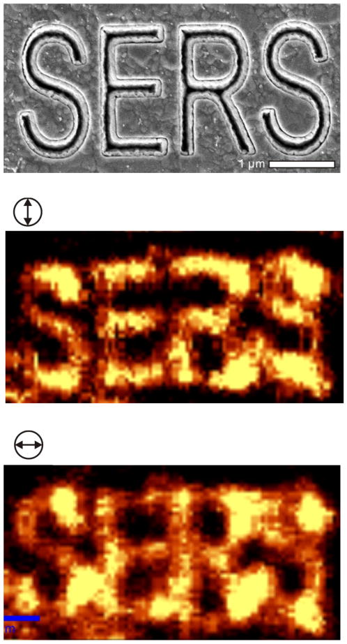
A key advantage of this scheme is that a dense array can be made over an entire wafer, and that it is straightforward to couple light into and out of the nanogaps. Vertically-oriented nanogap structures57 have been utilized in SERS as shown in Figure 6. It was shown that decreasing the gap size from 20 nm to 5 nm correlated to an increase in the Raman enhancement factor.57 Furthermore, it is possible to push the limits of this scheme to define gap sizes below 1 nm, which cannot be accomplished using other top-down fabrication techniques. High-throughput fabrication of atomic-scale gaps in metal films will provide new tools for basic research as well as practical applications in sensing, spectroscopy, nonlinear optics, and optical trapping.
Figure 6.
Confocal Raman imaging of nanogap structures formed along a “SERS” character pattern, showing the modulation of SERS hotspots along the polarization directions of an incident laser beam.
III. ALD for nanobiotechnology
Coating nanostructures with various materials via ALD can offer a number of advantages for surface modification, biocompatibility, and biosensing. In order to design a successful biosensor, the sensor surface should be amenable to straightforward surface-modification chemistry and be compatible with biological molecules. While some metals, like Au, are biologically inert and can be easily modified via self-assembled monolayers (SAMs), Ag or Cu suffers from poor biocompatibility. ALD layers, even on inert surfaces, are particularly useful for biological applications, allowing specialized surface functionalization such as lipid bilayer membranes.
ALD-grown silica shells for biosensing
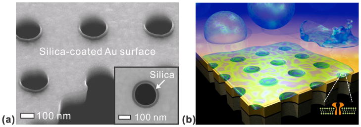
Gordon and co-workers developed an ALD process to deposit an extremely conformal SiO2 film with a small amount of impurities (Al2O3).58 A key advantage of this process is its superb conformality and a relatively low growth temperature (~ 250 °C). SiO2 surfaces are hydrophilic, biocompatible, and easily modified using well- established silane chemistry. For example, ALD-grown SiO2 was used to coat suspended Au nanopore arrays in order to support pore-spanning lipid bilayers59 as shown in Figure 7.
Figure 7.
(a) Cross-sectional SEM image of nanopores uniformly coated with a 20-nm-thick SiO2 layer to promote lipid bilayer formation (b) A schematic of a free-standing metallic nanopore array for sensing in a pore-spanning lipid bilayer environment. Adapted from Im et al.59
The motivation for creating suspended nanopores is to create a sensor that can be surrounded with a liquid buffer and that is more compatible with transmembrane proteins. The interaction of transmembrane proteins with underlying substrates can cause denaturation, changing the conformation of binding sites and complicating binding kinetic assays. In the suspended system, however, the planar lipid bilayer spans the pores and results in free-standing lipid bilayers that can efficiently incorporate transmembrane proteins.
Recently, free-standing nanopore arrays made in a thin Au/Si3N4 membrane were used for SPR biosensing with membrane proteins. There, the nanopore array was conformally coated with 20 nm-thick SiO2 by ALD (Figure 7).59 It was shown that the SiO2 layer on the nanopore array did not significantly reduce SPR sensitivity. Most importantly, the presence of SiO2 can induce the rupture of phospholipid vesicles to form planar lipid bilayers.60 Vesicles, also known as liposomes, are spherical lipid bilayers with adjustable dimensions (typical diameter: 50 nm 1–μm) depending on the preparation method used. When a SiO2 surface is exposed to a suspension of vesicles in solution, the vesicles will adsorb on the surface. When a critical surface population is reached, the vesicles begin to rupture forming a planar lipid bilayer on the SiO2 surface.61 A PDMS microfluidic chip was attached to the SiO2-coated nanopores for delivery of vesicles and reagents to the sensing area. By monitoring the spectral shift due to molecular binding as a function of time, it is possible to assess the binding kinetics and affinities of molecules to surface-bound targets. Real-time SPR sensing was performed using this platform and the transmembrane protein α-hemolysin (α-HL). The α-HL molecules selectively localized to the pore-spanning regions of the lipid bilayer, and SPR sensing was used to evaluate binding of an antibody to α-HL. The binding constants obtained with the method compared favorably with values obtained with alternative techniques.
Wittenberg et al. has demonstrated ALD coatings on silicon microwell and nanowell arrays to facilitate the assembly of biomembrane arrays.62 Because phospholipid vesicles will not rupture to form supported lipid bilayers on Al2O3 surfaces,63 vesicles and natural membrane particles can be arrayed without additional chemical modification of the substrate; nor do the natural membrane particles have to be modified in any way. These arrays were used for sensing interactions between proteins and lipid-based receptors in natural cell membranes. This strategy also enabled the formation of arrays of natural membranes in nanohole arrays in Au films, which allowed the use of SPR to detect antibody binding to cell-specific membrane receptors.
ALD to enhance analyte adsorption
To alter surface chemistry of metals while maintaining SERS activity requires thin molecular layers, like SAMs, or a thin-layer deposition technique such as ALD. In one such example, Van Duyne and coworkers used ALD Al2O3 on Ag nanostructures to improve SERS detection of a biomarker for anthrax spores, calcium dipicolinate (CaDPA).50 In this work they found that more CaDPA molecules adsorb to thin Al2O3 overlayers than adsorb to bare Ag nanostructures, which lowers the limit of detection (in terms of number of anthrax spores) from 2.6 × 10³ to 1.4 × 10³ spores. In addition, in competitive adsorption experiments it was found that CaDPA adsorbs to Al2O3 more strongly than structurally related molecules. This study also showed that Al2O3 overlayers can protect SERS substrates with no appreciably decline in performance after 9 months of storage in ambient conditions. This suggests that ALD coating of SERS substrates can make them more robust and suitable for long-term deployment and in-the-field analyses.
IV. Conclusion and Outlook
ALD has been a viable and widely utilized manufacturing method in the microelectronics industry. Currently, many research laboratories have access to reliable ALD tools, and the materials and processing options for ALD continue to expand. The growing field of plasmonics will increase the demand for new ALD processes to decorate various metallic surfaces at low temperatures. For the most part, existing applications in plasmonics and biotechnology have utilized Al2O3 or SiO2. In particular, metallic nanostructures that are overcoated with SiO2 shells can easily incorporate lipid bilayer membranes, which can be very useful for applications in 64, 65 biomimetic sensing and membrane proteins research. Other materials such as HfO2 or TiO2, which have higher refractive indices, could also be employed. While ALD for metals also looks promising for applications in plasmonics, impurities derived from the precursors remain in the metal. Thus metal films deposited by ALD exhibit poorer electrical and optical properties compared with pure metals deposited by evaporation or sputtering. As summarized in previous sections, the requirements for coating, patterning, tuning, and protecting metallic nanostructures are indeed very demanding. Metal surfaces, which are often rough and chemically unstable, should be modified at low temperatures with ultra-thin, pinhole-free overlayers. Conformal filling or complete encapsulation is required for nanostructures with extremely demanding aspect ratios. Finally, these ultra-thin films should act as a robust protection layer against harsh environments. ALD can readily satisfy all of these requirements and will continue to enable new and exciting applications.
Acknowledgments
This work was supported by grants to S.-H.O. from the Office of Naval Research (ONR Young Investigator Program), the National Science Foundation (NSF CAREER Award, CBET 1067681, DBI 0964216, DMR 0941537), the National Institutes of Health (NIH R01 GM092993), and a DARPA Young Faculty Award.
References
- 1.Ahonen M, Pessa M, Suntola T. A study of ZnTe films grown on glass substrates using an atomic layer evaporation method. Thin Solid Films. 1980;65:301. [Google Scholar]
- 2.Leskela M, Ritala M. Atomic layer deposition chemistry: Recent developments and future challenges. Angew Chem Int Edit. 2003;42:5548. doi: 10.1002/anie.200301652. [DOI] [PubMed] [Google Scholar]
- 3.Puurunen RL. Surface chemistry of atomic layer deposition: A case study for the trimethylaluminum/water process. J Appl Phys. 2005;97:121301. [Google Scholar]
- 4.George SM. Atomic layer deposition: An overview. Chem Rev. 2010;110:pv>111. doi: 10.1021/cr900056b. [DOI] [PubMed] [Google Scholar]
- 5.Mistry K, Allen C, Auth C, Beattie B, Bergstrom D, Bost M, Brazier M, Buehler M, Cappellani A, Chau R, Choi C-H, Ding G, Fischer K, Ghani T, Grover R, Han W, Hanken D, Hattendorf M, He J, Hicks J, Huessner R, Ingerly D, Jain P, James R, Jong L, Joshi S, Kenyon C, Kuhn K, Lee K, Liu H, Maiz J, McIntyre B, Moon P, Neirynck J, Pae S, Parker C, Parsons D, Prasad C, Pipes L, Prince M, Ranade P, Reynolds T, Sandford J, Shifren L, Sebastian J, Seiple J, Simon D, Sivakumar S, Smith P, Thomas C, Troeger T, Vandervoorn P, Williams S, Zawadzki K. A 45nm logic technology with high-k+metal gate transistors, strained silicon, 9 Cu interconnect layers, 193nm dry patterning, and 100% Pb-free Packaging. IEDM Tech Dig. 2007:247–250. [Google Scholar]
- 6.Bohr MT, Chau RS, Ghani T, Mistry K. The high-k solution. IEEE Spectrum. 2007;44:29. [Google Scholar]
- 7.Puurunen RL. Growth per cycle in atomic layer deposition: A theoretical model. Chem Vapor Depos. 2004;10:124. [Google Scholar]
- 8.Lim BS, Rahtu A, Gordon RG. Atomic layer deposition of transition metals. Nat Mater. 2003;2:749. doi: 10.1038/nmat1000. [DOI] [PubMed] [Google Scholar]
- 9.Maarit Kariniemi M, Niinistö J, Hatanpää T, Kemell M, Sajavaara T, Ritala M, Leskelä M. Plasma-enhanced atomic layer deposition of silver thin films. Chem Mater. 2011;23:2901. [Google Scholar]
- 10.Ritala M, Leskela M. Handbook of Thin Film Materials. Academic Press; San Diego: 2001. [Google Scholar]
- 11.Leskela M, Ritala M. Atomic layer deposition (ALD): from precursors to thin film structures. Thin Solid Films. 2002;409:138. [Google Scholar]
- 12.Kim H. Atomic layer deposition of metal and nitride thin films: Current research efforts and applications for semiconductor device processing. J Vac Sci Technol B. 2003;21:2231. [Google Scholar]
- 13.Niinisto L, Paivasaari J, Niinisto J, Putkonen M, Nieminen M. Advanced electronic and optoelectronic materials by atomic layer deposition: An overview with special emphasis on recent progress in processing of high-k dielectrics and other oxide materials. Phys Status Solidi A. 2004;201:1443. [Google Scholar]
- 14.Knez M, Niesch K, Niinistoe L. Synthesis and surface engineering of complex nanostructures by atomic layer deposition. Adv Mater. 2007;19:3425. [Google Scholar]
- 15.Kim H, Lee H-B-R, Maeng WJ. Applications of atomic layer deposition to nanofabrication and emerging nanodevices. Thin Solid Films. 2009;517:2563. [Google Scholar]
- 16.Wilk GD, Wallace RM, Anthony JM. High-k gate dielectrics: Current status and materials properties considerations,". J Appl Phys. 2001;89:5243. [Google Scholar]
- 17.Ritchie RH. Plasma losses by fast electrons in thin films. Phys Rev. 1957;106:874. [Google Scholar]
- 18.Barnes WL, Dereux A, Ebbesen TW. Surface plasmon subwavelength optics. Nature. 2003;424:824. doi: 10.1038/nature01937. [DOI] [PubMed] [Google Scholar]
- 19.Atwater H. The promise of plasmonics. Sci Am. 2007;296:56. [PubMed] [Google Scholar]
- 20.Polman A. Plasmonics Applied. Science. 2008;322:868. doi: 10.1126/science.1163959. [DOI] [PubMed] [Google Scholar]
- 21.Lal S, Link S, Halas NJ. Nano-optics from sensing to waveguiding. Nat Photonics. 2007;1:641–648. [Google Scholar]
- 22.Pelton M, Aizpurua J, Bryant G. Metal-nanoparticle plasmonics. Laser Photonics Rev. 2008;2:136. [Google Scholar]
- 23.Novotny L. From near-field optics to optical antennas. Phys Today. 2011;64:47. [Google Scholar]
- 24.Raether H. Surface plasmons on smooth and rough surfaces and on gratings. Springer- Verlag; 1986. [Google Scholar]
- 25.Homola J. Surface plasmon resonance sensors for detection of chemical and biological species. Chem Rev. 2008;108:462. doi: 10.1021/cr068107d. [DOI] [PubMed] [Google Scholar]
- 26.Cooper MA. Advances in membrane receptor screening and analysis. J Mol Recognit. 2004;17:286. doi: 10.1002/jmr.675. [DOI] [PubMed] [Google Scholar]
- 27.Armstrong SH, Jr, Budka MJE. Preparation and properties of serum and plasma proteins; the refractive properties of the proteins of human plasma and certain purified fractions. J Am Chem Soc. 1947;69:1747. doi: 10.1021/ja01199a050. [DOI] [PubMed] [Google Scholar]
- 28.Voros J. The density and refractive index of adsorbing protein layers. Biophys J. 2004;87:553. doi: 10.1529/biophysj.103.030072. [DOI] [PMC free article] [PubMed] [Google Scholar]
- 29.Jung LS, Campbell CT, Chinowsky TM, Mar MN, Yee SS. Quantitative interpretation of the response of surface plasmon resonance sensors to adsorbed films. Langmuir. 1998;14:5636. [Google Scholar]
- 30.Whitney AV, Elam JW, Zou SL, Zinovev AV, Stair PC, Schatz GC, Van Duyne RP. Localized surface plasmon resonance nanosensor: A high-resolution distance-dependence study using atomic layer deposition. J Phys Chem B. 2005;109:20522. doi: 10.1021/jp0540656. [DOI] [PubMed] [Google Scholar]
- 31.Im H, Lindquist NC, Lesuffleur A, Oh SH. Atomic layer deposition of dielectric overlayers for enhancing the optical properties and chemical stability of plasmonic nanoholes. ACS Nano. 2010;4:947. doi: 10.1021/nn901842r. [DOI] [PubMed] [Google Scholar]
- 32.Ebbesen TW, Lezec HJ, Ghaemi HF, Thio T, Wolff PA. Extraordinary optical transmission through sub-wavelength hole arrays. Nature. 1998;391:667. [Google Scholar]
- 33.Brolo AG, Gordon R, Leathem B, Kavanagh KL. Surface plasmon sensor based on the enhanced light transmission through arrays of nanoholes in gold films. Langmuir. 2004;20:4813. doi: 10.1021/la0493621. [DOI] [PubMed] [Google Scholar]
- 34.Dahlin A, Zäch M, Rindzevicius T, Käll M, Sutherland DS, Höök F. Localized surface plasmon resonance sensing of lipid-membrane-mediated biorecognition events. J Am Chem Soc. 2005;127:5043. doi: 10.1021/ja043672o. [DOI] [PubMed] [Google Scholar]
- 35.Tetz KA, Pang L, Fainman Y. High-resolution surface plasmon resonance sensor based on linewidth-optimized nanohole array transmittance. Opt Lett. 2006;31:1528. doi: 10.1364/ol.31.001528. [DOI] [PubMed] [Google Scholar]
- 36.Stewart ME, Mack NH, Malyarchuk V, Soares J, Lee TW, Gray SK, Nuzzo RG, Rogers JA. Quantitative multispectral biosensing and 1D imaging using quasi-3D plasmonic crystals. Proc Natl Acad Sci USA. 2006;103:17143. doi: 10.1073/pnas.0606216103. [DOI] [PMC free article] [PubMed] [Google Scholar]
- 37.Lesuffleur A, Im H, Lindquist NC, Oh SH. Periodic nanohole arrays with shape-enhanced plasmon resonance as real-time biosensors. Appl Phys Lett. 2007;90:243110. [Google Scholar]
- 38.Eftekhari F, Escobedo C, Ferreira J, Duan X, Girotto EM, Brolo AG, Gordon R, Sinton D. Nanoholes as nanochannels: Flow-through plasmonic sensing. Anal Chem. 2009;81:4308. doi: 10.1021/ac900221y. [DOI] [PubMed] [Google Scholar]
- 39.Im H, Lesuffleur A, Lindquist NC, Oh SH. Plasmonic nanoholes in a multichannel microarray format for parallel kinetic assays and differential sensing. Anal Chem. 2009;81:2854. doi: 10.1021/ac802276x. [DOI] [PMC free article] [PubMed] [Google Scholar]
- 40.Lindquist NC, Lesuffleur A, Im H, Oh SH. Sub-micron resolution surface plasmon resonance imaging enabled by nanohole arrays with surrounding Bragg mirrors for enhanced sensitivity and isolation. Lab Chip. 2009;9:382. doi: 10.1039/b816735d. [DOI] [PubMed] [Google Scholar]
- 41.Yang XD, Chen CJ, Husko CA, Wong CW. Digital resonance tuning of high-Q/V-m silicon photonic crystal nanocavities by atomic layer deposition. Appl Phys Lett. 2007;91:161114. [Google Scholar]
- 42.Qian LH, Shen B, Qin GWW, Das B. Widely tuning optical properties of nanoporous gold-titania core-shells. J Chem Phys. 2011;134:014707. doi: 10.1063/1.3523644. [DOI] [PubMed] [Google Scholar]
- 43.Jeanmaire DL, Van Duyne RP. Surface raman spectroelectrochemistry: Part I. Heterocyclic, aromatic, and aliphatic amines adsorbed on the anodized silver electrode. J Electroanal Chem. 1977;84:1. [Google Scholar]
- 44.Dieringer JA, McFarland AD, Shah NC, Stuart DA, Whitney AV, Yonzon CR, Young MA, Zhang XY, Van Duyne RP. Surface enhanced Raman spectroscopy: new materials, concepts, characterization tools, and applications. Faraday Discuss. 2006;1329 doi: 10.1039/b513431p. [DOI] [PubMed] [Google Scholar]
- 45.Groner MD, George SM, McLean RS, Carcia PF. Gas diffusion barriers on polymers using Al2O3 atomic layer deposition. Appl Phys Lett. 2006;88:051907. [Google Scholar]
- 46.Groner MD, Fabreguette FH, Elam JW, George SM. Low-temperature Al2O3 atomic layer deposition. Chem Mater. 2004;16:639. [Google Scholar]
- 47.Whitney AV, Elam JW, Stair PC, Van Duyne RP. Toward a thermally robust operando surface-enhanced Raman Spectroscopy substrate. J Phys Chem C. 2007;111:16827. [Google Scholar]
- 48.Sung J, Kosuda KM, Zhao J, Elam JW, Spears KG, Van Duyne RP. Stability of silver nanoparticles fabricated by nanosphere lithography and atomic layer deposition to femtosecond laser excitation. J Phys Chem C. 2008;112:5707. [Google Scholar]
- 49.Barrios CA, Malkovskiy AV, Kisliuk AM, Sokolov AP, Foster MD. Highly stable, protected plasmonic nanostructures for tip enhanced raman spectroscopy. J Phys Chem C. 2009;113:8158. [Google Scholar]
- 50.Zhang XY, Zhao J, Whitney AV, Elam JW, Van Duyne RP. Ultrastable substrates for surface-enhanced Raman spectroscopy: Al2O3 overlayers fabricated by atomic layer deposition yield improved anthrax biomarker detection. J Am Chem Soc. 2006;128:10304. doi: 10.1021/ja0638760. [DOI] [PubMed] [Google Scholar]
- 51.Nagpal P, Lindquist NC, Oh SH, Norris DJ. Ultrasmooth patterned metals for plasmonics and metamaterials. Science. 2009;325:594. doi: 10.1126/science.1174655. [DOI] [PubMed] [Google Scholar]
- 52.Im H, Lee SH, Wittengerg NJ, Johnson TW, Lindquist NC, Nagpal P, Norris DJ, Oh SH. Template-stripped smooth Ag nanohole arrays with silica shells for surface plasmon resonance biosensing,". ACS Nano. 2011;5:6244–6253. doi: 10.1021/nn202013v. [DOI] [PMC free article] [PubMed] [Google Scholar]
- 53.George SM, Ott AW, Klaus JW. Surface chemistry for atomic layer growth. J Phys Chem. 1996;100:13121. [Google Scholar]
- 54.Haynes CL, McFarland AD, Van Duyne RP. Surface-enhanced Raman spectroscopy. Anal Chem. 2005;77:338A. [Google Scholar]
- 55.Kneipp K, Wang Y, Kneipp H, Perelman LT, Itzkan I, Dasari RR, Feld MS. Single molecule detection using surface-enhanced Raman scattering (SERS) Phys Rev Lett. 1997;78:1667. [Google Scholar]
- 56.Nie SM, Emory SR. Probing single molecules and single nanoparticles by surface-enhanced Raman scattering. Science. 1997;275:1102. doi: 10.1126/science.275.5303.1102. [DOI] [PubMed] [Google Scholar]
- 57.Im H, Bantz KC, Lindquist NC, Haynes CL, Oh SH. Vertically oriented sub-10-nm plasmonic nanogap arrays. Nano Lett. 2010;10:2231. doi: 10.1021/nl1012085. [DOI] [PubMed] [Google Scholar]
- 58.Hausmann D, Becker J, Wang SL, Gordon RG. Rapid vapor deposition of highly conformal silica nanolaminates. Science. 2002;298:402. doi: 10.1126/science.1073552. [DOI] [PubMed] [Google Scholar]
- 59.Im H, Wittenberg NJ, Lesuffleur A, Lindquist NC, Oh SH. Membrane protein biosensing with plasmonic nanopore arrays and pore-spanning lipid membranes. Chem Sci. 2010;1:688. doi: 10.1039/C0SC00365D. [DOI] [PMC free article] [PubMed] [Google Scholar]
- 60.Keller CA, Kasemo B. Surface specific kinetics of lipid vesicle adsorption measured with a quartz crystal microbalance. Biophys J. 1998;75:1397. doi: 10.1016/S0006-3495(98)74057-3. [DOI] [PMC free article] [PubMed] [Google Scholar]
- 61.Anderson TH, Min Y, Weirich KL, Zeng H, Fygenson D, Israelachvili JN. Formation of supported bilayers on silica substrates. Langmuir. 2009;25:6997. doi: 10.1021/la900181c. [DOI] [PubMed] [Google Scholar]
- 62.Wittenberg NJ, Im H, Johnson TW, Lindquist NC, Nagpal H, Norris DJ, Oh SH. Facile assembly of micro- and nanoarrays for sensing with natural cell membranes. ACS Nano. 2011;5:7555–7564. doi: 10.1021/nn202554t. [DOI] [PMC free article] [PubMed] [Google Scholar]
- 63.Mager MD, Almquist B, Melosh NA. Formation and characterization of fluid lipid bilayers on alumina. Langmuir. 2008;24:12734. doi: 10.1021/la802726u. [DOI] [PubMed] [Google Scholar]
- 64.Frank MM, Wilk GD, Starodub D, Gustafsson T, Garfunkel E, Chabal YJ, Grazul J, Muller DA. HfO2 and Al2O3 gate dielectrics on GaAs grown by atomic layer deposition. Appl Phys Lett. 2005;86:152904. [Google Scholar]
- 65.Standridge SD, Schatz GC, Hupp JT. Toward plasmonic solar cells: Protection of silver nanoparticles via atomic layer deposition of TiO2. Langmuir. 2009;25:2596. doi: 10.1021/la900113e. [DOI] [PubMed] [Google Scholar]


