Abstract
Our research team has developed a 2D micro image display device that can potentially overcome the size reduction limits while maintaining the high-image resolution and field of view obtained by mirror-based display systems. The basic design of the optical scanner includes a microfabricated SU-8 cantilever waveguide that is electromechanically deflected by a piezoelectric actuator. From the distal tip of the cantilever waveguide, a light beam is emitted and the direction of propagation is displaced along two orthogonal directions. The waveforms for the actuator and the LED light modulation are generated and controlled using a field programmable gate array. Our recent study is an update to the previously-reported mechanical scanner, replacing the hand-built PZT scanner and fiber waveguide with a microfabricated system incorporating aerosol-deposited PZT thin film and a polymeric SU-8 wave guide. In this article, we report on the design and fabrication of a prototype miniaturized 2D scanner, discuss optical and mechanical the modeling of the system’s properties and present the experimental results.
Keywords: display system, SU-8 waveguide, MEMS, PZT thick film, aerosol deposition method
INTRODUCTION
Recently, new types of miniature scanner technologies used in see-through head mounted displays (HMD) have started to appear on the market. Among these new scanner technologies, the virtual retinal display developed at the University of Washington Human Interface Technology (HIT) Lab in the early 1990 s has been the most successful. Originally driven by acoustooptic scanners, it was later demonstrated and produced by Microvision using miniature scanner technologies, including microelectromechanical systems (MEMS) scanners. The display creates a virtual image at a viewer’s retina using raster scan image formed by laser or light-emitting diode (LED) light sources onto a bi-axial deflectable mirrors (Yan et al., 2003). This approach has many size limitations. For instance, light beams of less than few millimeters are impractical for displays using mirrors, because mirror scanners and grating deflectors must be significantly larger than the source light beam diameter to avoid beam clipping or adding diffraction. Reducing the diameter of a conventional display device reduces the possible number of pixels, and thus reduces the resolution and/or field of view (FOV) of the device. However, reduction in diameter and size enables construction of more comfortable HMDs and integration of display with other functional devices.
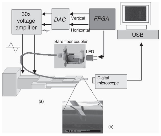
Our research team has previously developed a MEMS-based 2D micro image display device that can potentially overcome the size reduction limits while maintaining the high-image resolution and FOV obtained by mirror-based display systems. The optical scanner consists of a microfabricated waveguide that is electromechanically deflected by a 2D piezoelectric actuator (Wang et al., 2002; Takhashi et al., 2006). Modulated light emitting-diode (LED) light is guided through a fiber and coupled into the waveguide. From the distal tip of the cantilever waveguide, a light beam is emitted and the direction of propagation is displaced along two orthogonal directions. A developer board utilizing a Flex 10ETC30144-1 FPGA (1MHz external clock) drives the 2D piezoelectric actuator and modulates the LED light source. It is programmed to output three sets of signals, controlling the horizontal and the vertical frequency of the 2D actuator and the matching LED modulation. To generate the driving signals of the actuators, the Field-programmable Gate Array (FPGA) outputs an appropriate 8-bit signal to each channel at the rising edge of each clock cycle into a digital to analog converter. With an appropriate time sequence of 8-bit signals, a continuous triangular waveform at a desired frequency is output from the circuit. To provide sufficient driving voltages for the actuators, waveforms are then fed into a 30× amplifier. The FPGA also stores a matrix-formatted version of a desired image (converted from bitmap, 128 × 128). The FPGA processes the matrix and will light up the LED at corresponding 8-bit signal pair. Figure 1 shows the setup and the operational flow of the system.
Figure 1.
System key components diagram.
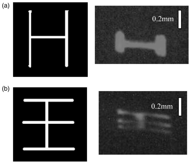
The pre-programmed image is then generated from the controlled oscillation of the actuator and the modulation of the LED (Figure 2). Minor distortions of original image are observed at the output due to the swept arc path of the resonating waveguide tip, which causes the image to stretch horizontally. However, this can potentially be corrected using digital image processing on the viewer’s side or by inserting an integrated lens system at the output end of the system.
Figure 2.
Input and output of the system along with corresponding images: (a) a letter “H” and (b) a Chinese character “
 ”.
”.
While functional, the original scanner design has a relatively large device footprint (each individual driving actuator is 20 × 4.8 × 0.6mm3) and it is difficult to replicate accurately. Although off-the-shelf PZT bimorph actuators provide ample display actuation, the original scanner is too large to be effective as part of a HMD, and the assembly of the device is difficult, time consuming, and unlikely to provide identical systems. The system also produces inconsistent results after each reset due to the way that the system is assembled, as it can be seen in Figure 2, the two images are already at different point of focus when reprogrammed. To standardize the devices and further improve the mechanical stability of the scanning, this report proposes a new design incorporating a PZT thin-film actuator and polymer-based cantilever waveguide, fabricated using MEMS processes. The prototype device will allow us to do a preliminary study on the aerosol-deposited PZT thin film, which will eventually be incorporated into our final design. In the following sections, we will present the numerical and experimental results of a prototype 2D MEMS optical scanner built from the proposed design.
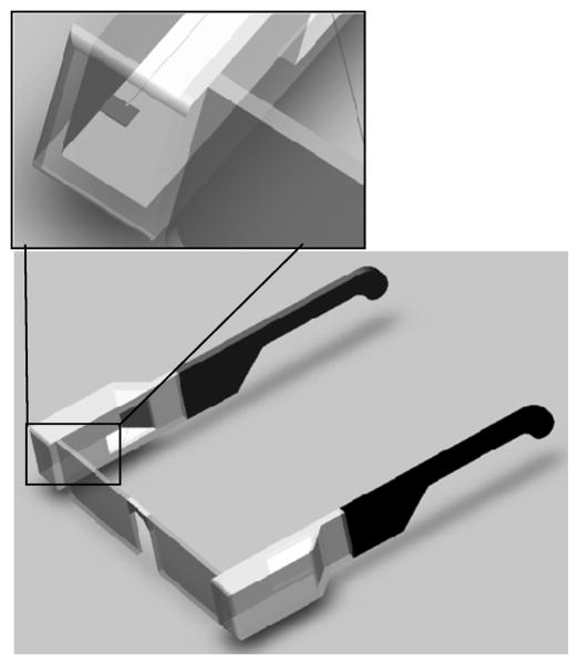
The microfabricated approach has several advantages. First, it allows for a shorter rigid scanner length, which is an important step for miniaturization of the display system. Second, this design makes batch production possible, and will result in lower fabrication costs while standardizing scanner quality. Finally, the integration of the actuators and waveguide into a single-small package (device footprint: 5 × 5mm2) opens up many interesting display designs to pursue (Figure 3).
Figure 3.
Scanner system integrated into a HMD system. Overall size and mass of the system is minimally affected.
DESIGN METHODOLOGY
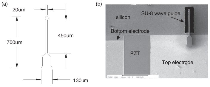
Our proposed microfabricated scanning device uses a fully integrated approach, where components are deposited in layers to create the final device. In our design, a 5-μm thick PZT thick film (with top and bottom electrode) is deposited on top of a silicon (Si) substrate. The Si substrate is designed to have two steps of thickness (320 and 143 μm). A SU-8 waveguide structure (Figure 4(a)) which is 470 μm long, 20 μm wide, and 100 μm thick is formed on top the PZT thick film at the thinner end of the silicon (Si) substrate. In the future, displacement sensors will be embedded near the tip of the scanner (Figure 4(b)). A piezoelectric thick film actuator in a tuning-fork-like configuration allows the scanner to create tip displacements in both vertical and horizontal directions; this is achieved by exciting its transversal and torsional vibration mode at the same time. The transversal mode of the actuator causes the waveguide to displace in the vertical direction due to the vertical motion of the actuator itself. The torsional vibration mode of the actuator introduces a horizontal motion on the waveguide due to the actuator’s rocking motion. Combing these two modes, a raster scanning motion can be produced and an image can be outputted following the same principles as our previous system. In the following sections, we detail the design of a prototype device to verify our hypothesis.
Figure 4.
(a) Dimensional layout of the SU-8 waveguide from the top and (b) overall layout.
Waveguide Design
In our design, we utilize SU-8 2100, a negative-tone epoxy-based photoresist (Microchem Corp.), as the waveguide structure. SU-8 waveguide structures are especially popular because they are easy to process and pattern; the material has the ability to produce high-aspect ratio vertical side-walls, and allows for dimensional control over the entire structural height. It is optically transparent for wavelength above 400 nm, which allows for guiding of visible lights. It creates a permanent structure after processing, producing a robust end product. The main goal of this design is to obtain a large-deflection angle at the tip of the SU-8 cantilever waveguide, which is actuated by a PZT-film actuator attached to the underside of the waveguide. The tapered structure at the base is designed to allow light from a regular 125 μm single-mode optical fiber to be easily coupled into the waveguide without additional optics. The subsequent tapering of the waveguide helps guide the light into the 19 × 95 × 450 μm3 cantilever section of the waveguide. The tip is a 20 × 20 μm2 diamond-shaped structure that creates a mass loading boundary condition at the tip to allow the reduction in tip displacement without losing deflection angle; it also acts as a lens at the output end of the waveguide to help focus the beam. The ratio between width and the thickness is designed to allow the waveguide to be driven at two resonance frequencies for 2D scanning motion because it gives rise to difference in stiffness in two directions. Adjusting the ratio will allow the resonance frequencies to be distinct, helping to avoid interferences that will generate unwanted behavior; it will also allow one driving frequency to be significantly lower than the other to generate the raster scanning effect with high resolution.
Actuator Design
A PZT thin film is used as the mechanical actuation for the SU-8 waveguide. The idea of using PZT is due to its high-piezoelectricity coefficient and Young’s modulus (Katz, 1959; Wada and Hayakawa, 1976), also the actuation mechanism is robust against environmental effects (e.g., humidity, temperature); additionally, because its manufacturing process is compatible with existing microfabrication processes, it is commonly used to provide mechanical actuation in MEMS devices. Currently, PZT thin films are generally fabricated with sol–gel process or sputtering technique (Lee et al., 2003; Jeon et al., 2003; Hsu et al., 2004; Kobayashi et al., 2006), each with their own disadvantages: sol–gel process is generally time consuming, and the quality of the resulting device is low compare to bulk PZT materials. Sputtering technique requires a target and a low-pressure environment. Therefore, for our device, we employed an unique deposition method based on aerosol (Lee and Wu, 2006) in order to produce high-quality PZT film. Films deposited with the aerosol technique have a thickness range from submicron to millimeter, good uniformity and low-surface roughness (<1 μm); also the film can be directly patterned during the deposition process. In the presence of an external applied voltage, the PZT thin-film structure changes shape producing dimensional changes in the material. Within certain range of electric and thermal stress, the voltage change V gives rise to a corresponding displacement L based on:
| (1) |
where S is strain (relative length change), L0 the ceramic length (m), E the electric field strength (V/m), and dij the piezoelectric coefficient of the material (m/V). Since the strain direction of the material is dependent upon the polarity of the external voltage, applying an alternating voltage to the device causes periodic expansion and contraction of the material, vibrating the actuator structure. Finally, the vibrating actuator excites the attached SU-8 waveguide, causing tip displacement. At different resonance frequencies, the actuator will be deformed into different mode shapes; this affects the deflection of the waveguide.
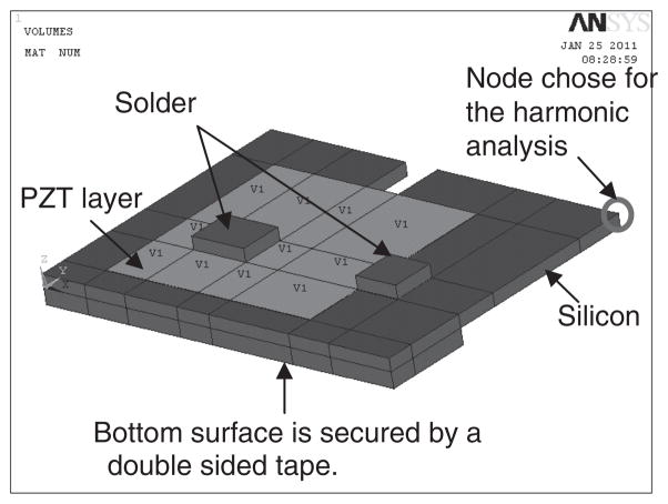
To predict the dynamics of the PZT scanner (a multilayer non-uniform geometric structure), we run finite element analysis (FEA) in ANSYS. The CAD model consists of silicon substrate, PZT thin film and two solder blocks. The solid model configurations and boundary conditions are shown in Figure 5. The top- and bottom-electrodes of the PZT are ignored due to the negligible thickness. The overall size of the device is only a few millimeter square, therefore, the solders are large enough to create significant effect on the output frequency response. The element SOILD5 is used to model the PZT and for the rest of the structures we used element SOLID45. The solder of each of electrode is modeled as a rectangular block. The bottom surface of the silicon of the thick section and the two blocks are fixed at all degree of freedoms. The block thickness is 0.15 mm. Table 1 lists the material properties used in the simulation.
Figure 5.
Configuration of model: silicon substrate, PZT thin film and two solder blocks. Each color indicates one material: purple is silicon, green is PZT, and red is solder.
Table 1.
Material properties used in ANSYS simulation.
| Young’s modulus (Mpa) | Density (kg/m3) | Possion’s ratio | |
|---|---|---|---|
| Silicon | 1.85 × 10⁵ | 2329 | 0.2 |
| Solder | 1 | 500 | 0.3 |
Device Fabrication
The device is fabricated on a single-sided polished p-type silicon wafer 〈100〉 orientation (Figure 6(a)). First, 200/1000Å Ti/Pt metal layers are deposited on the silicon substrate to form the PZT actuator’s bottom electrode using E-Beam deposition (Figure 6(b)). The PZT thick film is then applied using aerosol deposition and patterned with a lift-off process before sintering at 650°C (Figure 6(c)) in a furnace over 2 days and gradually cooling to room temperature. The film is annealed to reduce interface stress. After annealing, the top electrode which is 200/1000Å Cr/Au is deposited onto the PZT (Figure 6(d)). A 100-μm thick layer of SU-8 2100 is patterned onto the top electrode to form the optical structures of the scanner, including the cantilever waveguide, taper waveguide coupler, and lens (Figure 6(e)). Finally, the cantilever is released by the inductively coupled plasma (ICP) etching from the backside of the silicon substrate (Figure 6(f) and (g)). According to the previous poling process from our research team, a 5-μm PZT thin film should be poled at 44V (Lin, 2009). However, we were unable to pole our sample beyond 30V because the device started to break down. Therefore, we lower our poling voltage to 20V which is sufficient to pole the sample and produce the best eletromechnical coupling coefficient out of all the samples we have.
Figure 6.
Fabrication process of the cantilever.
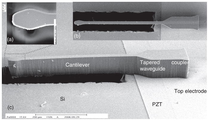
The SEM micrographs of the PZT actuated SU-8 waveguide scanner are shown in Figure 7. For our scanner design, the light is end butted into the waveguide from a laser with a pig-tailed single mode fiber. Here, the coupling is done by a tapered coupling waveguide system, where the end face cross-section on the fiber end is 130 × 130 μm2. Figure 7(a) shows a diamond-shaped tip. As shown in Figure 7(b) and (c), the geometry is designed such that the light of a regular 125 μm single-mode optical fiber can be easily coupled into the waveguide without any additional optical components. The subsequent tapering of the waveguide helps guide the light into the 19 × 95 × 450 μm3 suspended cantilever. The mass of the tip limits displacement while maintaining the angle of deflection. The diamond-shaped tip also helps focus the light beam. The thickness of the SU-8 waveguide is 95 μm, which is about 10 times larger than what we originally desired.
Figure 7.
SEM micrograph of the scanner system: (a) magnified view of the diamond-shaped lens, (b) top view of the optical structures showing the lens, cantilever, and tapered waveguide coupler, and (c) isometric view of the scanner structure.
The SEM photo in Figure 7(c) reveals a slight reduction in the geometry on the bottom of the SU-8 film. The reduction is mainly due to the thickness of the SU-8 layer, which makes uniform UV exposure difficult, as the light absorption is a function of penetration depth. This results in a slightly slanted sidewall. This problem can be minimized by tuning the duration of UV exposure, baking temperature, and baking time. In the prototype, the PZT film is measured to be around 4.95 μm thick. The surface and edges of the film appear smooth and uniform.
A deviation in the modal and displacement analysis between simulation and actual operation is expected to occur. This is because all polymer materials shrink after curing. From previous fabrication, we expect the SU-8 film to shrink around 5% after processing (Panergo et al., 2007). In this fabrication, we observe a reduction in the width of the cantilever beam of ~1.0 μm. The thickness is also reduced by about 5 μm. Although we use the recommended spin speed and development process for a 100-μm thick layer of SU-8, the cantilever is reduced to a thickness of 95 μm in the end. This result agrees with our previous finding. The displacement of the cantilever will also be hard to compare between the simulation and experiment because the damping effects from the air, structure, and material are unknown, making it difficult to accurately model the actual displacement. However, the input voltage versus the output displacement and deflection angle from the simulation and experiment should be linearly proportional, enabling the results of experimentation to be used to create a more accurate model of the system. In the near future, we plan to deposit a thicker film of SU-8 and revise the beam design to compensate the shrinkage in the SU-8.
One other likely cause for deviation between the simulation and experimental results is that a smaller than expected PZT actuation will be observed from the film actuator due to manufacturing process of the PZT film. Ideally, the PZT powders are dispersed by a sweeping technique during the deposition. In practice, the powders are more likely to collect with uneven distribution and create lumps or surface roughness. Additionally, the speed of deposit, the consumption of PZT powder, and the process time are not easy to control. Therefore, the resulting film thickness is not quite uniform, resulting in lower than expected throughput from the film.
RESULTS AND DISCUSSION
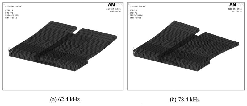
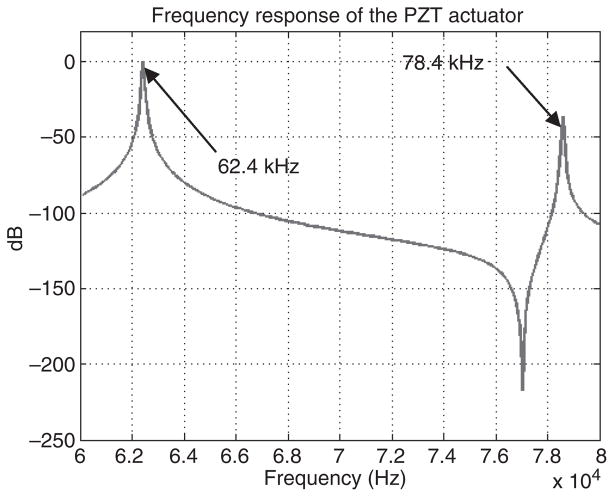
Simulation of the PZT actuator is done using commercially available FEA software ANSYS. We run the modal and harmonic analysis to predict the resonant frequencies of the PZT actuator and estimate the mechanical performance of the device. By taking the effect of the solders into consideration, the first two resonant frequencies of the actuator are 62.4 and 78.4 kHz, respectively. The corresponding mode shapes are shown in Figure 8. In harmonic analysis, a voltage of 10V is applied to the PZT. The frequency is swept from 60 to 80 kHz with an increment of 120 Hz. Figure 9 shows the resulting frequency response of the PZT actuator. The harmonic analysis verifies the modal analysis results and the designed PZT actuator is to be efficient to drive overall device at a low voltage.
Figure 8.
Mode shapes of the PZT actuator: (a) 1st mode shape and (b) 2nd mode shape.
Figure 9.
Frequency response of the actuator in z-direction.
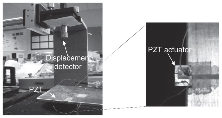
The experimental characterization of the micromachined device is conducted and the frequency response of the PZT actuator is measured using the fiber-optic based laser vibrometer system (Polytec, OFV 3001 and OFV 511). The displacement measurement setup is shown in Figure 10. Through the frequency modulation of back scattered light, the equipment is able to measure velocity as a function of time. Based on the velocity data the displacement response is deduced. The frequency response is generated by a swept sinusoidal signal with an amplitude of 2V. The signal is then amplified five times by the power amplifier (Instrumentation, type 790 series) before inputting to the PZT. The output displacement of the PZT actuator is converted into an electrical signal and analyzed by a two-channel dynamic analyzer (SRS, type 785 series).
Figure 10.
The displacement measurement setup utilizing a laser vibrometer.
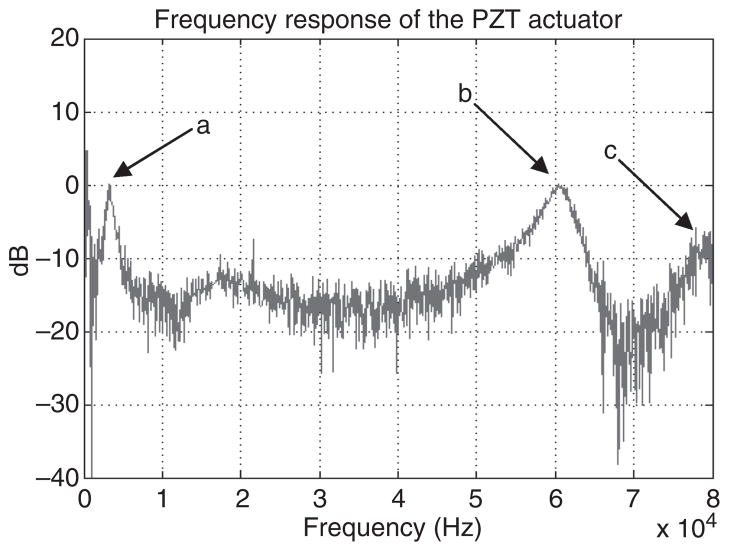
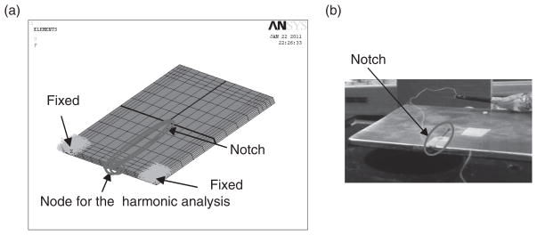
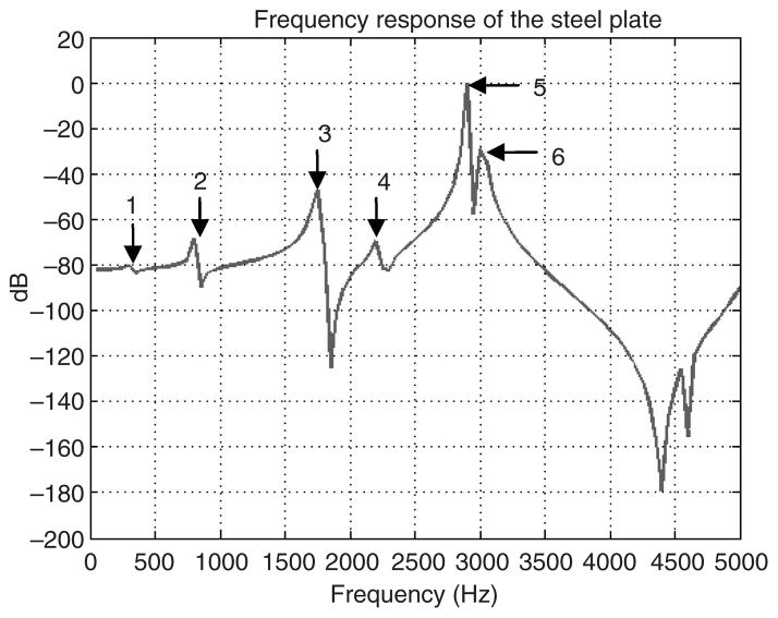
The experimental result of frequency response is shown in Figure 11. The first three resonant frequencies are 3.0, 60.1, and 77.8 kHz, respestively. However, ANSYS simulation in Figure 9 shows that the 3 kHz (peak a in Figure 11) is not one of the resonance peaks. We suspect that this frequency is one of the resonant frequencies from the supporting steel plate. Therefore, an investigation on the resonance frequencies of the steel plate is condcted. Here, the finite element model of the steel plate has a dimension of 11.7 × 11.7 × 0.5 cm3 with a 5.8 × 0.1 × 0.5 cm3 rectangular notch near where the PZT actuator is attached (Figure 12). The plate is secured to a table by a clamp on the opposite end. Table 2 lists the material properties of the steel plate. The frequency reponse spectrum obtained using harmonic analysis is shown in Figure 13. The node picked for the analysis is the location closest to where the PZT actuator is attached to the steel plate (Figure 12). Based on the anlysis, the first resonance of the steel plate occurs at 324 Hz (Figure 13). At the 5th resonance where it posses the most dominant displacement in z-direction, resonant frquency is 2.8 kHz which is quite close to the 3 kHz peak pick up by the laser vibrometer. It is most likely this is the one that get superimposed onto the frequency response of the PZT actuator.
Figure 11.
Measured frequency response of the piezoelectric actuator (displacement measurement taken from the location indicated in Figure 5). Peaks a–c are 3.0, 60.1, and 77.8 kHz, respectively.
Figure 12.
Steel plate: (a) 11.7 × 11.7 × 0.5cm3 CAD model with a 1 × 58mm2 notch and (b) photographic image of the steel plate.
Table 2.
Materaial properties of the steel plate.
| Density (kg/m3) | Young’s modulus (MPa) | Possion’s ratio |
|---|---|---|
| 7900 | 2 × 10⁵ | 0.3 |
Figure 13.
Frequency response of the steel plate. The frequency is from 0 to 5 kHz with 200 linearly spaced steps. Peaks 1–6 are 324, 815.3, 1.7, 2.2, 2.8, and 3.0 kHz, respectively.
The results from the modal analysis of the steel plate and the PZT actuator are compared with the experimental results (Table 3). From the results shown in Figures 11 and 13, we found that 3 kHz (peak a in Figure 11) is caused by one of the resonant frequencies of the steel plate, peaks b and c are the first two resonant frequencies of PZT actuator. The differences in frequencies are only off by 0.7–3.8%. We suspect that the differences are due to the clamping area and the thickness of the silicon substrate of the device not matching the values used in simulation and we consider this to be a very likely since the silicon thickness is measured only near the corner of the substrate, ignoring the possibility of non-uniform substrate thickness.
Table 3.
Results of resonant frequencies from experiment and simulation.
| Resonant frequencies | Experimental results (kHz) | Simulation results (kHz) | Difference (%) |
|---|---|---|---|
| Steel plate | 3.0 | 2.8 | 3.5 |
| PZT actuator | |||
| 1st | 60.1 | 62.4 | 3.8 |
| 2nd | 77.8 | 78.4 | 0.7 |
Frequencies observed at the location are shown in Figure 5.
The displacement can be calculated based on the velocity values from the dynamic analyzer. As shown in Figure 11, the actual input voltage (Vin) to the PZT actuator varies with frequency, due to impedance mismatch between the driving circuit and the actuator. Therefore, the equation for the maximum displacement, Dmax, takes the form:
| (2) |
where Vout is output voltage of laser vibrometer, f the driving frequency, and Vin the voltage input to the device.
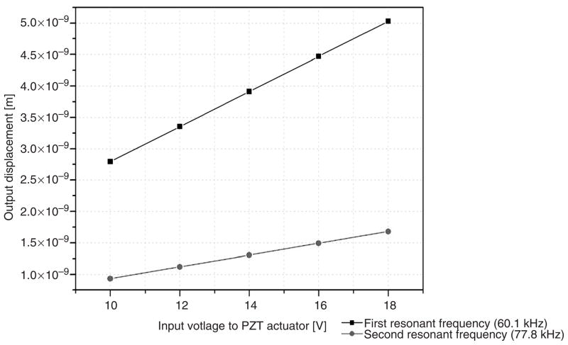
Since the width of the SU-8 waveguide is smaller than the laser beam profile of the laser vibrometer, the tip displacement of the PZT and its frequency response is measured instead. The displacement is measured at the corner of the PZT actuator as indicated in Figure 5. The resulting frequency response is shown in Figure 11. The maximum displacement is 5.02nm when the PZT is driven at its first resonant frequency (60.1 kHz) with an input voltage of 18V (Figure 14). The displacement of the actuator is relatively small, however, the waveguide geometry could be investigated in the final design to ensure that it will have sufficient deflection, and more importantly, sufficient deflection angle. In our final design, we will increase the deflection angle in several ways, such as increasing the aspect ratio of the waveguide cross-section, increasing the mass of the lens, increasing the cantilever length, or by increasing the applied voltage (without exceeding the poling voltage of 20 V). With new design currently under construction, the same PZT with different actuator configuration (e.g. push–pull design) has shown that it can generate a deflection angle greater than 12° with less than 10V input voltage driven at its first resonant frequency.
Figure 14.
The input votlage to PZT actuator vs output displacement cuve. Black line showing all the data taken at the first resonant frequency (60.1 kHz) and red line displaying the results from the second resonant frequency (77.8 kHz).
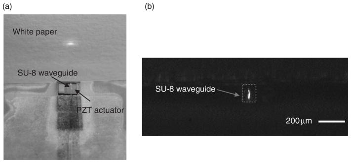
The light throughput from the SU-8 waveguide is tested using a 3-mW 632.8nm He–Ne laser coupled to a single-mode optical fiber (3 μm core, 125 μm cladding, Corning). The fiber is end butted to the waveguide structure. Figure 15 shows light emitted from the end of the waveguide. The light is clearly visible from the end. Figure 15(a) shows light reflected off a white piece of paper placed about 1 cm away from the tip of the waveguide. Based on a simple curve thick lens model, the focal length of the lens can be approximated by Equation (3):
| (3) |
where R is the radius of curvature of the lens, nlens and nair the refractive indices of the lens and air. Since the curvature is not uniform due to the limitations of the transparency mask, it is approximated to be around 40° μm. Thus, the focal length is calculated to be around 70 μm. The ideal focal length for one of the proposed retinal display system is around 4 cm. This can be easily adjusted by changing the curvature of the lens design.
Figure 15.
(a) Beam profile observed at some distance (~1 cm) away from the SU-8 waveguide and (b) light observed at the output of the cantilever waveguide (image rotated 90°).
Due to lack of a proper light detection system, the light coupling efficiency is not measured. Although we know the absorption of the SU-8 film is considerably low (<0.3 dB/cm) (Wang et al., 2003), we did observe some light loss due to scattering from the rough sidewalls of the SU-8 waveguide (Figure 16). This can be attributed to the developing and baking process is not being optimized and ICP over etching during the release. We expect that once the fabrication parameters are controlled, the roughness of the sidewall can be reduced down to <10nm as shown in the reference (Panergo et al., 2007).
Figure 16.
Top view of optical waveguide cantilever, the length of the beam is 450 μm from the support to the tip.
CONCLUSIONS
In this article, we have presented the concept of miniaturizing a 2D optical scanning system based on a mechanically resonating SU-8 waveguide actuated by a thick film piezoelectric actuator. Using our proposed process, we successfully fabricate a PZT thick-film actuator using the aerosol deposition method, with a polymeric SU-8 waveguide formed on top of the structure. The SU-8 waveguide shows good qualitative optical performance with some light loss, which can be corrected by calibrating the fabrication parameters to produce smoother sidewalls. Experimental results of the prototype demonstrated waveguide and actuator displacement when an AC input voltage is applied and simulation results indicated that 2D actuation can be achieved by simultaneously driving the device at two distinct resonance frequencies. Currently, the performance of the actuator does not meet the necessary specifications for a fully functional display system. This may be caused by control errors in the fabrication process resulting in non-uniform PZT film thickness, and it is also possible that the necessary film thickness is underestimated. To address these issues and improve the system, we will revise our design and manufacturing process. Specifically, using a thinner, wider, rib-shaped waveguide will reduce our output beam size while maintaining the aspect ratio of the cross-section. This also resolves the issue of sidewall tapering caused by thick structures. To amplify the push–pull effect that generates 2D scanning based on 1D actuation, we will modify the prototype’s tuning-fork-like actuator design to a “double wing” structure. Combining the improved design with a thicker PZT layer and thinner silicon substrate, we expect significant improvement in system performance and 2D scanning capability. In anticipation of future work and application research, additional structures will be integrated into the scanner, including a fiber groove for better coupling to the light source and a displacement sensor to allow feedback control of the system, further improving system stability.
Acknowledgments
This study was supported in part by the NIH grant R01 EB007637. Special thanks to Benjamin Estroff and William Soetanto (University of Washington) for their assistance with fabrication and collecting experimental results.
References
- Hsu Y-C, Wu CC, Lee CC, Cao GZ, Shen IY. Demonstration and Characterization of PZT Thin-Film Sensors and Actuators for Meso- and micro- Structures. Sensors and Actuators A: Physical. 2004;116:369–377. [Google Scholar]
- Jeon YS, Steyn R, Kim S. Energy Harvesting MEMS Devices Based on d33 Mode Piezoelectric Pb(Zr, Ti)O3 Thin Film Cantilever. Proceedings of CIRP Seminar on Micro and Nano Technology; 13–14 November; Copenhagen, Denmark. 2003. [Google Scholar]
- Katz HW. Solid State Magnetic and Dielectric Devices. Wiley; New York: 1959. pp. 94–126. [Google Scholar]
- Kobayashi T, Tsaur T, Ichiki M, Maeda R. Fabrication and Performance of a Flat Piezoelectric Cantilever Obtained Using a Sol-gel Derived PZT Thick Film Deposited on a SOI Wafer. Journal of Smart Material Structures. 2006;15:S137–S140. [Google Scholar]
- Lee B, Wu W. Tunable Resonant Frequency Power Harvesting Devices. SPIE Proceedings 6169, Smart Structure and NDE Conference; San Diego, CA. 2006. [Google Scholar]
- Lee SH, Ryu MK, Kim JP, Kim SR, Heo JY, Jang MS. Ferroelectric Properties of PZT Thin Films Deposited on ZnO/Si Substrates. Journal of Korean Physical Society. 2003;42:S1105–S1107. [Google Scholar]
- Lin S. Master Thesis. National Taiwan University; 2009. Design, Fabrication and Evaluation of 2D Structure Piezoelectric MEMS Generator. [Google Scholar]
- Panergo R, Huang CS, Liu CS, Reinhall P, Wang WC. Resonant Polymeric Optical Waveguide Cantilever Integrated for Image Acquisition. Journal of Lightwave Technology. 2007;25:850–860. [Google Scholar]
- Takahashi C, Wang H, Hua W, Reinhall P, Wang W. Polymeric Waveguide Design of 2D Display System. SPIE Proceedings 6177, SPIE NDE Health Monitoring and Diagnostics; San Diego, CA. 2006. [Google Scholar]
- Wada Y, Hayakawa R. Piezoelectricity and Pyroelectricity of Polymers. Japanese Journal of Applied Physics. 1976;15:2041–2057. [Google Scholar]
- Wang W, Fauver M, Ho J, Seibel EJ, Reinhall PG. Micromachined Optical Waveguide Cantilever as a Resonant Optical Scanner. Sensors and Actuators A: Physical. 2002;102:165–175. [Google Scholar]
- Wang W, Panergo R, Reinhall P. Development of a Microfabricated Scanning Endoscope Using SU-8 Based Optical Waveguide Machined Optical Waveguide. Proceedings of SPIE 5047, Smart Nondestructive Evaluation and Health Monitoring of Structural and Biological Systems II; 15–17 March; San Diego, CA. 2003. pp. 305–313. [Google Scholar]
- Yan J, Luanava S, Casasata V. Magnetic Actuation for MEMS Scanners for Retinal Scanning Displays. SPIE Proceeding 4985, MOEMS Display and Imaging Systems; San Jose, USA. 2003. pp. 115–120. [Google Scholar]


