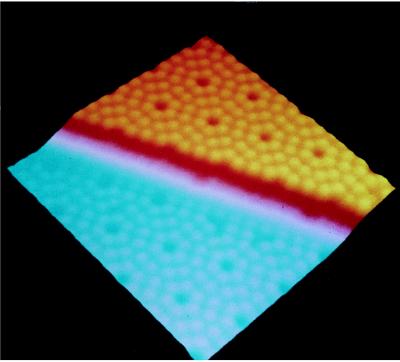
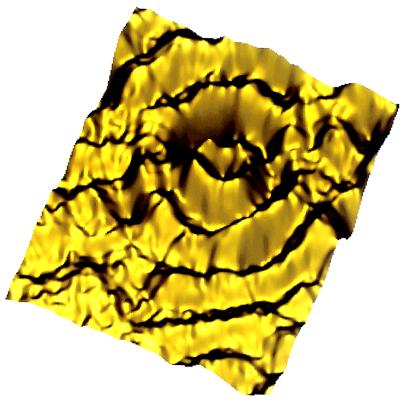
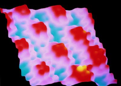
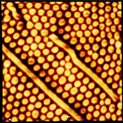
The imaging and manipulation of matter at the scale of individual atoms has been a long-standing dream that has become reality since the scanning tunneling microscope (STM) was invented by Gerd Binnig and Heinrich Rohrer, who received the Nobel Prize for Physics in 1986 (1). In STM and related scanning probe methods, a probe tip of atomic sharpness is brought within close proximity to the object under investigation until some physical signal can be measured that might originate from electronic, electrical, magnetic, optical, thermal, or other kinds of interactions between tip and sample. Point probing by a sharp tip allows one to receive local information about the physical, chemical, or biological state of a sample, which facilitates the investigation of site-specific sample properties. By scanning the probe tip relative to the sample under investigation by means of piezoelectric drives, a spatially resolved map of the sample in the light of the particular type of selected interaction is obtained. To achieve high spatial resolution the distance s between the probe tip and the sample is chosen to be smaller than the characteristic wavelength λ of the particular type of interaction acting between tip and sample. (In the case of STM, λ would be the electron wavelength, whereas for a scanning optical microscope, λ would be the optical wavelength.) In this so-called near-field regime (where s < λ), the spatial resolution is no longer limited by diffraction but rather by geometrical parameters: the distance s between the probe tip and the sample surface, and the effective radius of curvature R of the probe tip. STM and related scanning probe methods are therefore exceptional types of microscopes because they work without lenses (in contrast to optical and electron microscopes) and achieve “super-resolution” beyond the Abbé limit. For strongly distance-dependent interactions, the dominant tip–sample interaction region can be as small as a few Ångstroms, thereby allowing the imaging of individual atoms and molecules on surfaces (Fig. 1). This new experimental technique has led to several textbook (2) examples of real-space observations of quantum phenomena, such as the interference of electron waves in the vicinity of atomic impurities (Fig. 2), in “quantum corrals” (4), or in low-dimensional solids exhibiting charge density waves (Fig. 3). Further remarkable applications include the observation of micromagnetic structures by magnetic probe microscopy (Fig. 4) or chemical reactions by STM (7).
Figure 1.
Perspective STM image showing a step edge on a single-crystalline Si surface. The periodic arrangement of the atoms persists up to the step edge except for single-point defects. Adapted from ref. 3.
Figure 2.
Perspective scanning conductance image of electron waves scattered at a dopant atom in InAs. The data were taken at 8 K. Scanned area: 75 nm × 65 nm. Adapted from C. Wittneven, R. Dombrowski, M. Morgenstern, and R. Wiesendanger, unpublished results.
Figure 3.
Perspective STM image of a TaSe2 surface showing a periodic charge density wave pattern superimposed on the atomic lattice. Scanned area: 14 nm × 14 nm. Adapted from ref. 5.
Figure 4.
Magnetic bubble structure observed by magnetic force microscopy with a magnetized tip. Apart from the circular-shaped magnetic bubble domains, two stripe domains are visible that are caused by two scratches in the surface topography (not shown). Scanned area: 60 μm × 60 μm. Adapted from ref. 6.
Another important feature of scanning probe microscopes is that they can be operated in air and in liquids as well as in a vacuum, which offers novel opportunities for high-resolution studies of the structure and processes at solid–fluid interfaces. In particular, in situ electrochemical studies and in vivo investigations of organic molecules and biological specimen at unprecedented real-space resolution have become some of the more recent intense fields of applications (8, 9), in addition to surface science studies under ultra-high vacuum conditions. Because scanning probe instruments can also be operated under physiological conditions, they have proven to be ideally suited to solve questions in life sciences. Recently, scanning probe methods have even evolved into a platform technology for mechanical experiments with individual molecules (10–12). In these experiments, a suitable substrate is covered with a layer of polymer molecules functionalized with receptor molecules that can be picked up by the probe tip covered with ligands. During the following stretching cycle both the elasticity of the stretched molecules and the unbinding forces of the molecular couplers can be measured.
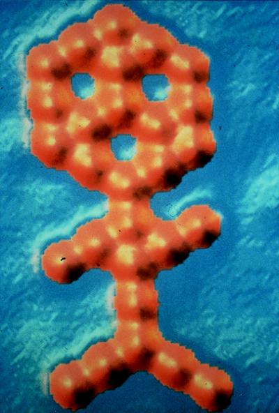
The concept of increasing the interaction strength between probe tip and sample in a controllable manner has become important for the fabrication of well-defined nanometer-scale structures (13). It has even become possible to synthesize artificial structures by sliding individual atoms and molecules on surfaces by means of the probe tip (Fig. 5). The controlled manipulation of matter at the scale of individual atoms and molecules might lead to new generations of nanoelectronic and mass storage devices. On the other hand, scanning probe instruments have also become very powerful metrological devices that allow to measure, for example, distances between objects with atomic accuracy (15). The high accuracy of distance measurements offered by scanning probe methods is also of great importance for a variety of sensor applications (16).
Figure 5.
“Molecular man,” built from 28 CO molecules, measuring 45 Å from head to foot. The sliding of the CO molecules on the Pt substrate was achieved by lowering the tip of a scanning tunneling microscope, thereby increasing the interaction strength between the tip and the adsorbed molecules. Image courtesy of P. Zeppenfeld, C. P. Lutz, and D. M. Eigler. Adapted from ref. 14.
In summary, there seems to be an unlimited number of applications of scanning probe microscopes used as imaging, measuring, sensing, or manipulation devices. The possibility of creating artificial material structures on an atom-by-atom basis is currently exploited for sophisticated experiments in the new nano-laboratories. Concepts of future devices that make use of these fascinating new possibilities have just started to be developed. The evolution of scanning-probe-based science and technology is continuing to be an exciting excursion into a small world.
Acknowledgments
I thank Hermann E. Gaub and Joseph Zasadzinski for their help in preparing this manuscript.
Footnotes
The Frontiers of Science symposia is the latest in the series “From the Academy,” which is presented occasionally to highlight work of the Academy, including the science underlying reports of the National Research Council.
References
- 1.Binnig G, Rohrer H. Rev Mod Phys. 1987;59:615. [Google Scholar]
- 2.Wiesendanger R. Scanning Probe Microscopy and Spectroscopy: Methods and Applications. Cambridge, U.K.: Cambridge Univ. Press; 1994. [Google Scholar]
- 3.Wiesendanger R, Tarrach G, Bürgler D, Güntherodt H-J. Europhys Lett. 1990;12:57. [Google Scholar]
- 4.Crommie M F, Lutz C P, Eigler D M. Science. 1993;262:218. doi: 10.1126/science.262.5131.218. [DOI] [PubMed] [Google Scholar]
- 5.Wiesendanger R, Anselmetti D. In: Scanning Tunneling Microscopy I. 2nd Ed. Güntherodt H-J, Wiesendanger R, editors. Berlin: Springer; 1992. p. 131. [Google Scholar]
- 6.Wadas A, Wiesendanger R, Novotny P. J Appl Phys. 1995;78:6324. [Google Scholar]
- 7.Avouris P, Wolkow R. Phys Rev B. 1989;39:5091. doi: 10.1103/physrevb.39.5091. [DOI] [PubMed] [Google Scholar]
- 8.Wiesendanger R, Güntherodt H-J, editors. Scanning Tunneling Microscopy II. Berlin: Springer; 1992. [Google Scholar]
- 9.Takamoto, D. Y., Ter-Ovanesyan, E., Schwartz, D. K., Viswanathan, R., Chiruvolu, S. & Zasadzinski, J. A. (1997) Acta Phys. Pol., in press.
- 10.Rief M, Oesterhelt F, Heymann B, Gaub H E. Science. 1997;275:1295. doi: 10.1126/science.275.5304.1295. [DOI] [PubMed] [Google Scholar]
- 11.Floring E-L, Moy V T, Gaub H E. Science. 1994;264:415. doi: 10.1126/science.8153628. [DOI] [PubMed] [Google Scholar]
- 12.Moy V T, Floring E L, Gaub H E. Science. 1994;266:257. doi: 10.1126/science.7939660. [DOI] [PubMed] [Google Scholar]
- 13.Wiesendanger R. Appl Surf Sci. 1992;54:271. [Google Scholar]
- 14.Zeppenfeld P, Lutz C P, Eigler D M. Ultramicroscopy. 1992;42–44:128. [Google Scholar]
- 15.Teague E C. J Vac Sci Technol. 1989;B7:1898. [Google Scholar]
- 16.Wiesendanger R. In: Micro- and Nanosensor Technology/Trends in Sensor Markets. Meixner H, Jones R, editors. New York: VCH; 1995. [Google Scholar]


