

Abstract
We experimentally demonstrated photonic crystal microcavity based resonant sensors coupled to photonic crystal waveguides in silicon nano-membrane on insulator for chemical and bio-sensing. Linear L-type microcavities are considered. In contrast to cavities with small mode volumes, but low quality factors for bio-sensing, we showed increasing the length of the microcavity enhances the quality factor of the resonance by an order of magnitude and increases the resonance wavelength shift while retaining compact device characteristics. Q~26760 and sensitivity down to 15 ng/ml and~110 pg/mm2 in bio-sensing was experimentally demonstrated on silicon-on-insulator devices.
In recent years, integrated optical devices have been developed to function as microarrays for chemical and biological assays. Platforms based on ring resonators [1], wire waveguides [2] and surface plasmon resonance (SPR) [3] have been investigated. The detection principle in all instances is based on the specific binding of the biomolecule of interest to its specific conjugate biomolecule receptor bound to the optical device substrate causing a change in the refractive index and in the transduced signal. While it is possible to design sensors with ultra-small mode volumes [4], current biomolecule patterning technologies limit the minimum spacing between resonators in an array when each sensor is coated with a unique biomolecule receptor. Inkjet printing techniques [5] enable denser integration compared to methods using microfluidic channels where laminar flow considerations make miniaturization challenging below 100 μm for effective biomolecule patterning [2].
Photonic crystals (PCs) are a relatively new platform generating significant interest over the last decade because of their ability to confine light to ultra-small mode volumes and their high sensitivity to changes in refractive index of the ambient promising the potential for creating high-density microarrays. Various designs of PC microcavities have been proposed for chemical [6] and bio-sensing [7] using microcavities with small mode volumes. Radiation losses, however, increase with increasing refractive index of the ambient significantly reducing the resonance quality (Q) factor due to reduced out-of-plane confinement in two-dimensional PCs. Thus, although high Q-factors have been demonstrated in freely suspended PC membranes in air [4], which promises the potential for highly sensitive sensing in air, when such membranes are suspended in phosphate buffered saline (PBS) (refractive index n = 1.334), a typical ambient for biomolecules, Q-factors deteriorate by orders of magnitude. Hence, researchers have attempted optimum designs balancing two contradictory requirements: increasing the Q-factor of the resonance versus increasing the wavelength shift due to change in refractive index. In passive silicon PC nanostructures, the transmission drop-resonance architecture has been used predominantly with hexagonal [7] and linear PC microcavity coupled to a W1 photonic crystal waveguide (PCW). The best results have been achieved in freely suspended membranes [8], which are fragile structures. In this paper, we present high Q PC microcavities in silicon nano-membrane on insulator structures for bio-sensing microarray applications. Since radiation losses are inversely proportional to the cavity size and because of fundamental biomolecule patterning limitations in microarrays, we investigated methods to increase device sensitivity by increasing the size of the PC microcavity while retaining the compactness of PC structures.
The PCW is a hexagonal structure with a W1 line defect waveguide with uniform lattice constant a = 400 nm, where W1 denotes PCW width PCW of . Silicon slab thickness and air hole diameter are h = 0.58a and d = 0.54a as shown in Fig. 1(a).A microscope image of a patterned device with an array of two PC microcavities is shown in Fig. 1(b). Detailed characteristics of the arrayed device are under evaluation and will be covered in another publication. In this paper, we consider single PC microcavity sensors only. In Fig. 1(b), we note that by inkjet patterning, the minimum dispensed spot size of biomolecules is ~35 μm. The inkjet dispensed spot size determines the minimum spacing between adjacent sensors. It is different from the device surface area functionalized by combining lithographic patterning with inkjet printing [5]. PC microcavities of gradually increasing length were investigated to characterize resonance line widths and sensitivity.
Fig. 1.
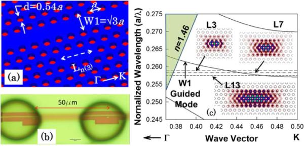
(a) Device schematic. (b) Inkjet printed biomolecules on PC devices showing spacing between printed spots (scale bar is 10 μm). (c) Dispersion diagram of W1 PCW in water. The W1 guided mode is shown together with frequencies of resonant modes for L3, L7 and L13 PC microcavities by dashed lines. Respective mode profiles are shown in insets.
Linear PC microcavities Ln, where n presents the number of missing holes along Γ − K direction, are fabricated two periods away from the PCW. The edge air holes are shifted in the Γ − K direction by 0.15a [4]. Fig. 1(c) shows a band structure obtained by three-dimensional plane-wave expansion simulations of the W1 PCW, considering water (n 1.33) as the ambient. The normalized resonance frequencies of different PC microcavities of increasing lengths obtained by 3D finite-difference time domain simulations are indicated by dotted lines in Fig. 1(b). The resonant mode profiles are shown in the insets.
Light is guided in and out of the PCW by ridge waveguides with PC group index taper to enable high coupling efficiency into the slow light guided mode [9]. Devices were fabricated on silicon-on-insulator (SOI) wafer using established methods [9]. The bottom cladding of silicon dioxide (n 1.46) is kept intact enabling robust devices with high yield. Devices were tested with TE-polarized light by end-fire coupling method with polarization maintaining single mode tapered lensed fibers. The transmission drop resonance Q and sensitivity to bulk refractive index changes are analyzed with water and isopropyl alcohol (IPA) (n 1.377) as the ambient medium. Figs. 2(a)–(c) show experimental transmission spectra from W1 PCWs with coupled L3, L7 and L13 PC microcavities in water. In Figs. 2(d)–(f), drop transmission of the resonance closest to the band edge, as in insets of Fig. 1(b), for L3, L7 and L13 PC microcavities in water and IPA are shown.
Fig. 2.
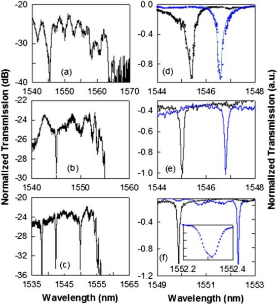
Experimental W1 PCW transmission spectrum in water with coupled (a) L3 (b) L7 and (c) L13 microcavities. Experimental spectra showing shift of resonance mode closest to the band edge in (a), (b) and (c) in (d), (e), and (f) respectively in water (black) versus IPA (blue). Inset (e) magnifies the wavelength range.
Fig. 3 shows resonance shifts Δλ observed experimentally with the device in water versus in IPA. Figure 3 also plots experimental Q (= λ/Δλ) in water and IPA, at the center frequency, and the approximate resonance offset ΔΛ from the W1 transmission band edge. It is observed from Fig. 3 as the resonance moves closer to the band edge of the W1 PCW, Q and Δλ increase. Since IPA does not absorb in the wavelength range studied, Q in IPA is higher than in water.
Fig. 3.
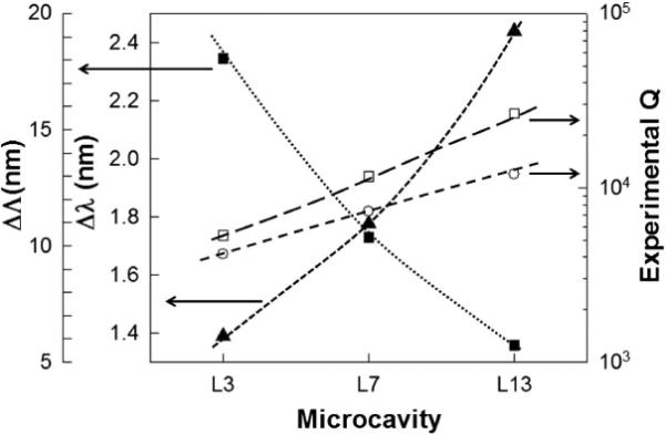
Plots showing trends in L3, L7 and L13 PC microcavities for resonant mode (a) quality factor in water (open circle) (b) quality factor in IPA (open square) (c) approximate mode offset from the transmission band edge (filled square, left offset axis) and (d) wavelength shift from water to IPA (filled triangle, left axis).
The increase in Q as the resonance approaches increasing group index near the band edge is the result of the combined effect of cold cavity Q, caused by the inverse dependence of radiation loss on cavity size [4], and the diverging waveguide density of states [10] in the coupled cavity-waveguide system as the resonance moves deeper into the photonic band gap, thereby increasing the fraction of the electromagnetic field below the light line. Due to increase in mode volume, the resonance mode overlaps with more air holes along the borders of the cavity, leading to higher Δλ. By microcavity engineering, the highest Q~26760 was observed in a L13 PC microcavity in a SOI device with sensitivity (S) ~52 nm/RIU (RIU=refractive index unit). S is calculated as S = Δλ/Δn from values in water and IPA. Similar sensitivities were achieved in single-period resonators in SOI with Q ~450 [11]. The high Q in our device improves measurement resolution for the detection of smaller changes in concentration.
The enhanced sensitivity and resolution is next applied to bio-sensing. Wafers were functionalized by treating with 1 mg/mL poly-L-lysine in water, followed by washing three times in PBS. Wafers were then incubated in 1% glutaraldehyde in PBS for five minutes, inkjet printed with target antibodies (Abs), and washed three times in PBS. 60 μl of probe Ab was directly dispensed from a micro-pipette. The diameter of the dispensed spot on silicon. is ~8 mm
Instead of the final resonance shift as in Ref. [12], after each new concentration of probe Ab, the devices are washed in PBS and the resonance wavelength measured. While surface binding of target Ab can also be used to characterize device sensitivity, the resonance wavelength shift of interest for such hybrid assays is shown by Δλ in Fig. 4(a), which measures the probe antigen containing the predefined spectral response specifically bound to the target Ab. In Fig. 4(b), the magnitude of resonance shift as a function of rabbit anti-goat (molecular weight MW 150 KDa) binding to Goat Abs and Rat monoclonal Ab (MW 150 KDa) binding to Human IL-10 Abs is plotted for L3 and L7 microcavities, respectively. As in chemical sensing, higher Q 300 and larger sensitivity is observed for L7 than L3 PC microcavities. This represents the highest Q reported for bio-sensing in SOI PC devices. The spectral shift when 0.1 nM of Rat monoclonal Ab is added is shown in the inset. We experimentally detected binding of 0.1 nM or 15 ng/ml of probe Ab with L7 devices. Since dn/dT = 1.87 × 10⁻⁴ at 295 K for silicon, if we consider a maximum variation of 1 K in temperature, the biomolecule sensing measurement limit of the shift Δλ is 0.01 nm from the measured bulk sensitivity. The extrapolated concentration detection limit with L7 devices is thus ~20 pM. In Fig. 1(c) inset, with a sensing area ~6.2 μm2, (integrating over an area where the E-field intensity is more than 50% of maximum value and including the internal surface area of holes) [13], dispensed probe Ab volume of 60 μl over a diameter of 8 mm, and assuming uniform surface coverage, the estimated mass detection limit, without considering unbound Abs that are washed away, in L7 devices is ~10.6 ag. The detection limit for surface density is ~22 pg/mm2, which compares favorably with detection limits of 1 pg/mm2 in SPR, on more than four orders of magnitude smaller area [3]. The detection limit also compares favorably with 60 pg/mm2 estimated in ref. [12]. Experimentally, we detected 110 pg/mm2 of bound antibody. Actual bound mass will be much lower since a significant fraction is washed away. It is also expected that L13 devices will show higher sensitivity to bound antibody due to the larger mode overlap with surrounding air holes. Further measurements are in progress.
Fig. 4.
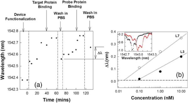
(a) Resonance wavelength of L3 PC microcavity at different steps in the binding sequence. The resonant wavelength shift of interest is denoted by Δλ. (b) Resonance shift of L3 (filled circles) and L7 PC microcavities (open circles) with probe antibody binding. Dashed line indicates the detection limit. Inset shows peak wavelength shift on binding. (inset) Normalized intensity data showing shift in L7 microcavity resonance from black to red curve upon addition of 0.1 nM probe antibodies.
In summary, we demonstrated a method for bio-sensing coupling high Q resonance and high sensitivity in SOI PC devices. The wave-guiding nature of our device enables denser chip-scale miniaturization than SPR microarrays with the ability to probe multiple devices simultaneously for high throughput measurements.
Acknowledgments
The authors acknowledge the National Cancer Institute for supporting this work under the SBIR program (contract # HHSN261201000085C). Silicon nano-membrane device related work was sponsored by the AFOSR MURI (Contract # FA9550-08-1-0394).
Reference
- 1.Iqbal M, Gleeson MA, Spaugh B, Tybor F, Gunn WG, Hochberg M, Baehr-Jones T, Bailey RC, Gunn LC. IEEE J. Sel. Top. Quantum Electron. 2010;16:654. [Google Scholar]
- 2.Densmore A, Vachon M, Xu DX, Janz S, Ma R, Li YH, Lopinski G, Delage A, Lapointe J, Luebbert CC, Liu QY, Cheben P, Schmid JH. Opt. Lett. 2009;34:3598. doi: 10.1364/OL.34.003598. [DOI] [PubMed] [Google Scholar]
- 3.Sipova H, Zhang S, Dudley AM, Galas D, Wang K, Homola J. Anal. Chem. 2010;82:10110. doi: 10.1021/ac102131s. [DOI] [PMC free article] [PubMed] [Google Scholar]
- 4.Akahane Y, Asano T, Song B-S, Noda S. Nature. 2003;425:944. doi: 10.1038/nature02063. [DOI] [PubMed] [Google Scholar]
- 5.Tan CP, Cipriany BR, Lin DM, Craighead HG. Nano Lett. 2010;10:719. doi: 10.1021/nl903968s. [DOI] [PMC free article] [PubMed] [Google Scholar]
- 6.Chakravarty S, Topoľančik J, Bhattacharya P, Chakrabarti S, Kang Y, Meyerhoff ME. Opt. Lett. 2005;30:2578. doi: 10.1364/ol.30.002578. [DOI] [PubMed] [Google Scholar]
- 7.Lee M, Fauchet PM. Opt. Express. 2007;15:4530. doi: 10.1364/oe.15.004530. [DOI] [PubMed] [Google Scholar]
- 8.Kang C, Phare CT, Vlasov YA, Assefa S, Weiss SM. Opt. Express. 2010;18:27930. doi: 10.1364/OE.18.027930. [DOI] [PubMed] [Google Scholar]
- 9.Lin C-Y, Wang X, Chakravarty S, Lee B-S, Lai W-C, Chen RT. Appl. Phys. Lett. 2010;97:183302. [Google Scholar]
- 10.Waks E, Vuckovic J. Opt. Express. 2005;13:5064. doi: 10.1364/opex.13.005064. [DOI] [PubMed] [Google Scholar]
- 11.Pal S, Guillermain E, Sriram R, Miller BL, Fauchet PM. Biosens. Bioelectron. 2011;26:4024. doi: 10.1016/j.bios.2011.03.024. [DOI] [PMC free article] [PubMed] [Google Scholar]
- 12.Scullion MG, Di Falco A, Krauss TF. Biosens. Bioelectron. 2011;27:101. doi: 10.1016/j.bios.2011.06.023. [DOI] [PubMed] [Google Scholar]
- 13.Dorfner D, Zabel T, Hurlimann T, Hauke N, Frandsen L, Rant U, Abstreiter G, Finley J. Biosens. Bioelectron. 2009;24:3688. doi: 10.1016/j.bios.2009.05.014. [DOI] [PubMed] [Google Scholar]