Abstract
Scalable circuits of organic logic and memory are realized using all-additive printing processes. A 3-bit organic complementary decoder is fabricated and used to read and write non-volatile, rewritable ferroelectric memory. The decoder-memory array is patterned by inkjet and gravure printing on flexible plastics. Simulation models for the organic transistors are developed, enabling circuit designs tolerant of the variations in printed devices. We explain the key design rules in fabrication of complex printed circuits and elucidate the performance requirements of materials and devices for reliable organic digital logic.
The promise of ubiquitous computing1 has inspired researchers to integrate electronic circuits into everyday objects and biological tissues2. The vision is for distributed sensors and processing devices to monitor and respond to the environment autonomously, enhancing the way humans interact with objects around them. For example, sensors incorporated into clothing or attached to skin can allow continuous monitoring of vital signs and alert people, both locally and remotely, if dangerous thresholds are exceeded. To enable widespread penetration of these systems, the electronic hardware must be inexpensive and minimally intrusive. Printed electronic components provide mechanical flexibility and stretchability3,4,5 as well as low-cost manufacturability, complementing the computing power of silicon electronics.
Two key elements that can enable complex printed circuits are logic and memory. Organic semiconductors are particularly suitable for printed logic because they can be processed in solution6,7. Recently, organic thin-film transistors (OTFTs) with performance comparable to that of inorganic amorphous silicon TFTs have been reported8,9. Organic circuits have been fabricated using photolithographic processes10,11, which offer high reliability but are incompatible with high-throughput, low-cost manufacturing methods, such as roll-to-roll processing. Fundamental circuit building blocks, such as inverters and differential pairs12,13, as well as a non-rewritable RFID tag14 have been demonstrated in a printed process, representing first steps towards more complex circuits.
Combining logic and rewritable memory can enhance the capability of printed electronics. The inclusion of memory allows identification or history information to be maintained. Non-volatile ferroelectric memory in passive and active matrix arrays15,16,17 has been demonstrated. The addition of addressing logic is necessary for these arrays to be scalable: a binary logic decoder allows 2N rows in an array to be controlled with just N-bits. The provides a scalable addressing scheme for matrix arrays common in electronics and is widely applicable to arrayed sensor and display applications.
In this work, we use additive fabrication processes that are entirely compatible with roll-to-roll print manufacturing to demonstrate small-scale complex circuits. An inkjet-patterned 3-bit memory decoder is realized for addressing ferroelectric memory capacitors. The all-additive process includes both n- and p-type organic semiconductors, enabling the utilization of complementary logic to reduce power consumption and improve circuit stability. We describe our device models and use of simulation-based design, essential for complex circuits. We explain the key challenges in fabrication of complex printed circuits and elucidate the minimum performance requirements of materials and devices for reliable digital logic. Finally, we present the results of combining the decoder with ferroelectric capacitors, to demonstrate a scalable memory array with integrated logic.
Results
Decoder design
The structural disorder inherent in thin-film semiconductor leads to challenges in the design and fabrication of robust organic TFT circuits, because the disorder limits charge transport and reduces uniformity across devices18. In addition, dynamic trapping of mobile charge in band-tail states results in decreasing channel current at constant bias over time19,20,21. Device variability and bias-stress instability are measured and accounted for in the development of accurate device models, which in turn facilitate the design of robust circuits.
Printed OTFT characteristics
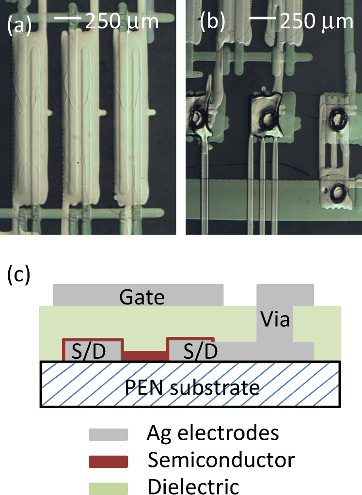
Figure 1 shows microphotographs of printed OTFTs along with a schematic illustration of an OTFT cross-section. The transistors are bottom-contact top-gate structures on plastic polyethylene naphthalate (PEN) substrates. The width of printed silver lines is 65 ±5 μm. The line-to-line spacing is 35 ±5 μm, which also defines the transistor channel length. In the process used here, layer-to-layer registration accuracy is 15 μm. As shown in Fig. 1(a), the gate electrode is designed to completely overlap the interdigitated source/drain (S/D) electrodes. This configuration increases overlap capacitance, reducing the speed of the device. However, it also greatly reduces the risk of un-gated channel regions resulting from misalignment. Furthermore, it serves as a light shield to reduce photogenerated off-current. The via between source/drain and gate layers is formed by laser ablation of the dielectric layer followed by silver overprinting [Fig. 1(b)].
Figure 1.
Microphotographs of (a) printed OTFTs and (b) via connections. (c) Schematic of an OTFT cross-section.
The availability of p- and n-type semiconductors with comparable performance enables the use of complementary logic. Complementary logic gates have wider noise margins than their unipolar equivalents22. Furthermore, complementary gates partially self-compensate for bias-stress instability23, minimizing the need for compensation circuits24,25 used with unipolar logic.
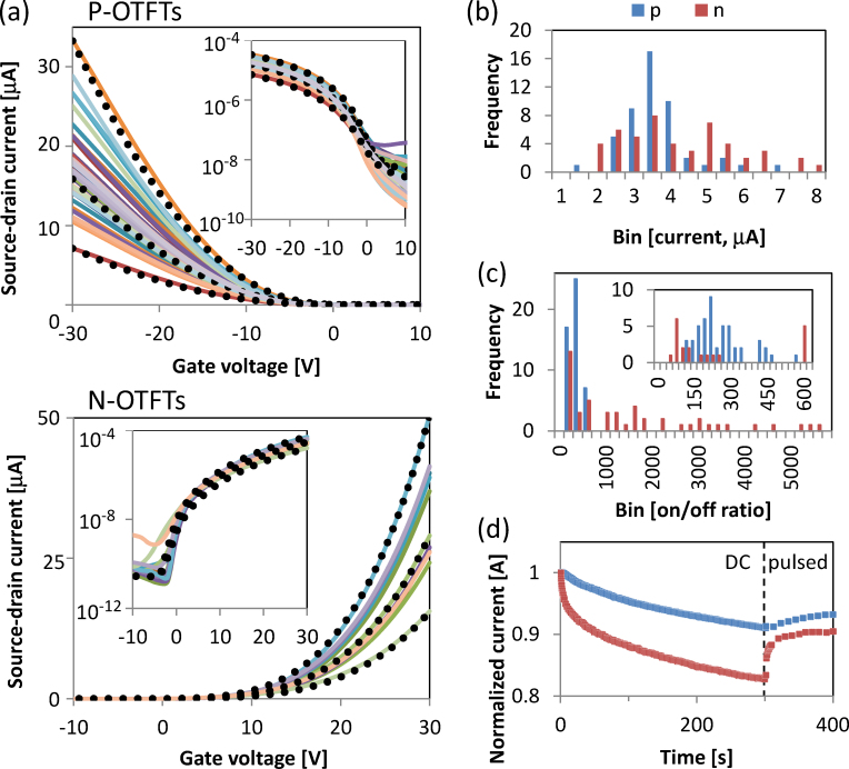
The key transistor performance parameters for logic design are the on current and the on/off current ratio. The transfer characteristics of p- and n-channel OTFTs are shown in Fig. 2. In each type of device, for given bias conditions, there is a six-fold device-to-device variation in drain current. This level of variability is comparable to that of photolithographically defined organic transistors10, indicating that printing-specific factors, such as inconsistent source-drain spacing, represent only a minor contribution. The primary sources of the variability are morphology and thickness variations in the semiconductor film, which are observed in both printed and photolithographic processes.
Figure 2.
(a) Transfer characteristics of printed p- and n-channel OTFTs, with channel length of 2.75 mm and width of 35 μm, in saturation regime Vds = ±20 V and Vgs = ±20 V. The dotted lines represent best-fit models for slow, typical, and fast OTFTs. Histograms of current distribution (b) and on/off ratio (c) were taken from measurements in linear regime Vds = ±5 V and Vgs = ±20 V for lower bound estimation. (d) Normalized current during operation with Vds = ±20 V and Vgs = ±20 V at constant gate bias or at pulsed gate bias of 1 kHz, 50% duty cycle.
Linear regime characteristics are used to determine the minimum device on/off ratio. For the gate voltage range of 0 V to ±20 V, the minimum on/off ratio is 100 for p-channel OTFTs and 75 for n-channel OTFTs. The histogram in Fig. 2(c) shows the spread of on/off ratios for both types of device. The distribution is observed to be more compact for p-type devices. This is the result of better thickness uniformity as the parameter spread is partially dependent on semiconductor thickness.
The effect of bias stress is shown in Fig. 2(d). In both device polarities, the current decreases by up to 20% with both gate voltage Vgs and source-drain voltage Vds held at a constant ±20 V bias for 5 minutes. The n-channel transistor showed faster current decrease than the p-channel device, and one explanation for the current degradation is charge trapping in the band-tail states18,19,20,21. In many circuits, including the design presented here, most transistors are not held in static states, but continually switch during operation. In this case, only those traps with longer time constants than the average switching period contribute to the effective threshold voltage shift associated with bias stress, while faster traps are released during the OTFT off time. This is shown in Fig. 2(d) where the drain current recovers by 5–10% when the static gate bias is switched to a 1 kHz square wave.
Modeling printed OTFTs
As the behavior of OTFTs differs significantly from that of metal-oxide-semiconductor field-effect transistors (MOSFETs), standard silicon MOSFET models are not appropriate for OTFT simulation. Behavioral models have been proposed26, but these are computationally expensive and show unreliable convergence. TFT-specific SPICE models, such as those for amorphous silicon (a-Si) devices, while not intended for organic devices, have similar characteristics and are sufficiently parameterized to allow reliable models to be developed27. A description of the model may be found at http://www.ece.uci.edu/docs/hspice/hspice_2001_2-179.html. The models are only semi-physical and empirical curve-fitting must be employed to generate accurate curves.
Models of the organic TFTs based on measured transfer curves have been developed using the RPI a-Si model. In this model, the drain current is given by
In these equations, Ci is the gate capacitance, W and L are the channel width and length, respectively, VGS is the gate-source potential, VT is the threshold voltage, and VDSe is the effective drain-source potential. The parameters αS, VAA, μn, and γ are constants, with VAA having units of volts, and μn nominally the mobility at the threshold voltage. In practice, neither this mobility nor the threshold voltage is well defined for OTFTs, but these parameters can be used along with the other constants to fit the model to experimental data.
Device-to-device variability is incorporated into the SPICE models using process corners. The convention of “slow”, “typical”, and “fast” corners is used. Additional corners can be defined for variations such as low on/off ratios and excessive leakage current. The main sources of variation in printed OTFTs (semiconductor morphology and thickness) are linearly related to drain current, which, in the RPI model, is linearly dependent on the parameter μn (MUBASE in some variations of SPICE). Once a “typical” model is developed, “fast” and “slow” corner models can created by scaling μn appropriately. With the models developed by varying μn, Fig, 2(a) shows simulated transfer characteristics of slow, fast, and typical devices overlaid with experimental measurements. The key model parameters are listed in Table 1.
Table 1. Key OTFT model parameters.
| TFT type | Ci [nF cm−2] | αs [unitless] | VAA [V] | γ [unitless] | μn [m2 V−1 s−1] |
|---|---|---|---|---|---|
| p-channel | 5 | 0.45 | 3000 | 0.37 | 2.2×10⁻⁵ (“S”) |
| 5.5×10⁻⁵ (“T”) | |||||
| 1.0×10⁻⁴ (“F”) | |||||
| n-channel | 5 | 0.25 | 223 | 2.1 | 5.0×10⁻⁴ (“S”) |
| 1.1×10⁻³ (“T”) | |||||
| 1.7×10⁻³ (“F”) |
The OTFT models do not directly account for time-variant behavior such as bias-stress instability and must be modified to include these dynamic effects. Such temporal variation can be modeled in transient analyses with time-dependent voltage and current sources. This approach can yield accurate results but is computationally expensive because of the time-scale mismatch between logic functionality (microseconds to milliseconds) and bias stress (minutes to days). Instead, here the dynamic effects in the OTFT models are counted as augmented process variation, by shifting the threshold voltages until the transfer characteristic matches that of a stressed device. Only minor adjustments to the models are needed in accounting for the dynamic effects, considering that the magnitude of bias stress is significantly less than that of static device-to-device variability.
Decoder schematics and simulation
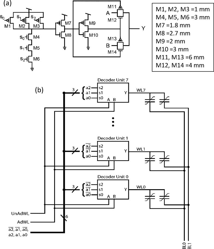
Figure 3(a) shows the circuit diagram of a decoder unit comprising a 3-input NAND gate (M1-M6), two inverting buffers (M7/M8, M9/M10), and two transmission gates (M11/M12, M13/M14), for a total of fourteen OTFTs per decoder unit. The function of the circuit is to pass signal B to the output Y if and only if signals s0, s1, and s2 are all high, and to pass signal A to Y otherwise. In the context of a ferroelectric memory array, A is the unaddressed word line signal, B is the addressed word line signal, and Y is connected to one of the word lines of a memory array. A 3-bit decoder [Fig. 3(b)] is constructed by combining eight of these units. Each word line is selected by a unique triplet combination of s0, s1, s2, or their complements.
Figure 3.
Circuit diagrams of (a) an individual decoder sub-unit, with OTFT channel length of 35 ±5 μm and channel widths listed on the right, and (b) a 3-bit decoder with eight sub-units.
The 3-bit decoder is configured to address a memory array with eight word lines and two bit lines. Each transmission gate is designed to drive 70 pF, corresponding to the combined maximum capacitance of two memory cells, from 0 V to the cell drive voltage of Vdr = 16 V within 3 ms. Due to the low on/off ratio of the OTFTs, the pair of transmission gates acts in effect as a resistive divider. In addition, the shunt leakage conductance of the memory cells, specified to be no greater than 33 nS, is non-negligible relative to the on-conductance of the transmission gates. The combination of these properties determines the minimum gate width as well as the input voltage overhead needed to obtain the correct output level. Increasing the width of the transmission gates increases the on-conductance and, in turn, the circuit speed. However, the speed levels off when the channel capacitance of the transmission gate dominates the capacitance of the load. This defines a practical upper bound to the gate width for a given capacitive load.
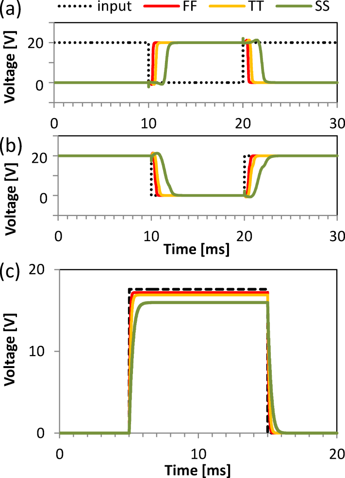
From circuit simulations, the fan-out-of-one delay is found to be approximate 0.5 ms for the fastest OTFTs and approximately 0.85 ms for the slowest OTFTs. Figures 4(a) and 4(b) show the timing from a NAND-input signal (s0) edge to the transmission gate control signals using both “FF” (fast-fast) and “SS” (slow-slow) process corners. The “FF” corner switches fully in 1 ms and to VDD/2 in 400 μs. The “SS” corner switches fully in 2.6 ms and to VDD/2 in 2 ms. Figure 4(c) shows simulated waveforms of transmission gate signals. Because of the low on/off ratio of the OTFTs and the shunt conductance of the memory cells, 17.6 V must be applied to the selected transmission gate input to achieve the desired 16 V output in the “SS” process corner. With this same overdrive, the output of a transmission gate in the “FF” corner is 17.2 V; the increased output voltage is acceptable for this memory decoder application.
Figure 4.
Simulation outputs of (a) NAND logic and (b) NAND logic with inverter. (c) Simulation outputs of transmission gates.
Static logic requires sufficient contrast between the lowest on-current and highest off-current in a given logic gate. For the printed static decoder here, the logic gates are observed to function reliably with current contrast ratios of twenty or more, although other circuit designs might require better ratio. This contrast ratio parameter is distinct from the on/off ratio of an individual OTFT. As illustrated in Fig. 2, devices commonly show similar on/off ratios but widely divergent on- and off-currents. Therefore, with a current variability of six times in both p- and n-channel OTFTs, a minimum on/off ratio of 120 for individual OTFTs is required to guarantee a current contrast ratio of twenty. To develop robust logic circuits, further improvement is desirable as yield directly impacts the number of transistors that can be included in a circuit. Simple redundancy can also be utilized to obtain more working units but adversely impacts circuit area and speed.
Integration of decoder and ferroelectric memory
Addressing scheme to write/read memory
The memory elements are capacitors with a ferroelectric poly(vinylidene fluoride)-based copolymer as the dielectric. The ferroelectric film retains remnant polarization without an applied electric field and the polarization state functions as non-volatile memory. Properties of ferroelectric memories such as retention time, read-write durability, and environmental stability have been documented in References16,28. Table 2 shows the parameters of the printed memory cells used in this study. Here we demonstrate the addressing of the memory cells with an integrated decoder.
Table 2. Printed memory characteristics.
| Switching polarization | 15 μC/cm2 |
| Non-switching polarization | 2 μC/cm2 |
| Remnant polarization PR | 13 μC/cm2 |
| Coercive field Ec | 70 MV/m |
A memory cell is written to the 0 or 1 state, respectively, by the application of a positive or negative potential across the capacitor. By convention, the potential is taken to be relative to the word line. In the read process, the memory state is discerned by measuring the quantity of charge released during application of a negative bias29, with more charge released for a 0 state than for a 1 state. Since the potential applied during reading would also set the cell to the 1 state, this is a destructive read process.
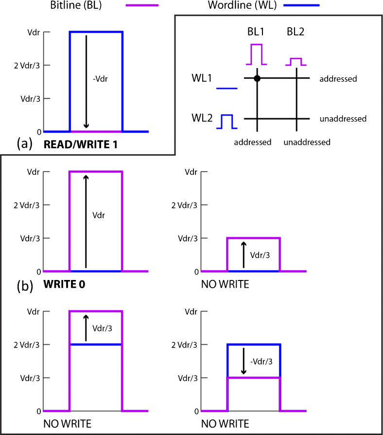
In a memory array, each word line and bit line are connected to multiple cells. To prevent unintentional disturbs during read and write events, the potential across unaddressed cells must be kept below a threshold, nominally one-third of the writing voltage, Vdr. One method to accomplish this is to actively drive addressed and unaddressed word lines and bit lines with the signals shown in Fig. 5. In the read process, all memory cells on the selected word line are read simultaneously by individual charge integrators. The bit lines and unaddressed word lines are held at ground while the addressed word line is driven to Vdr. During reading, all cells connected to the addressed word line are set to 1, the default state. To write a cell to 0, its word line is set to ground and its bit line to Vdr. All unaddressed word lines are held at  and all unaddressed bit lines are held at
  . With these waveforms, the absolute potential across any unaddressed cell is at most
  and is below disturb threshold. A 2×2 array is the smallest memory that requires the full set of read/write waveforms in Fig. 5. As such, it is the minimum memory size required to demonstrate scalability.
Figure 5.
Voltage input to memory word lines and bit lines during (a) the read/reset/write 1 or (b) the write 0 process.
Signal measurements
A photograph of the decoder connected to the memory array is shown in Fig. 6(a). To match the 12-word-line memory array, the decoder was fabricated with twelve sub-units, four of which have redundant addresses. Experimental verification of decoder functionality is demonstrated in Fig. 6(b). With input A held at a constant value, the decoder unit passes the switching signal from input B to output Y only when it is addressed. With any other combination of address signals, the output Y is floating.
Figure 6.
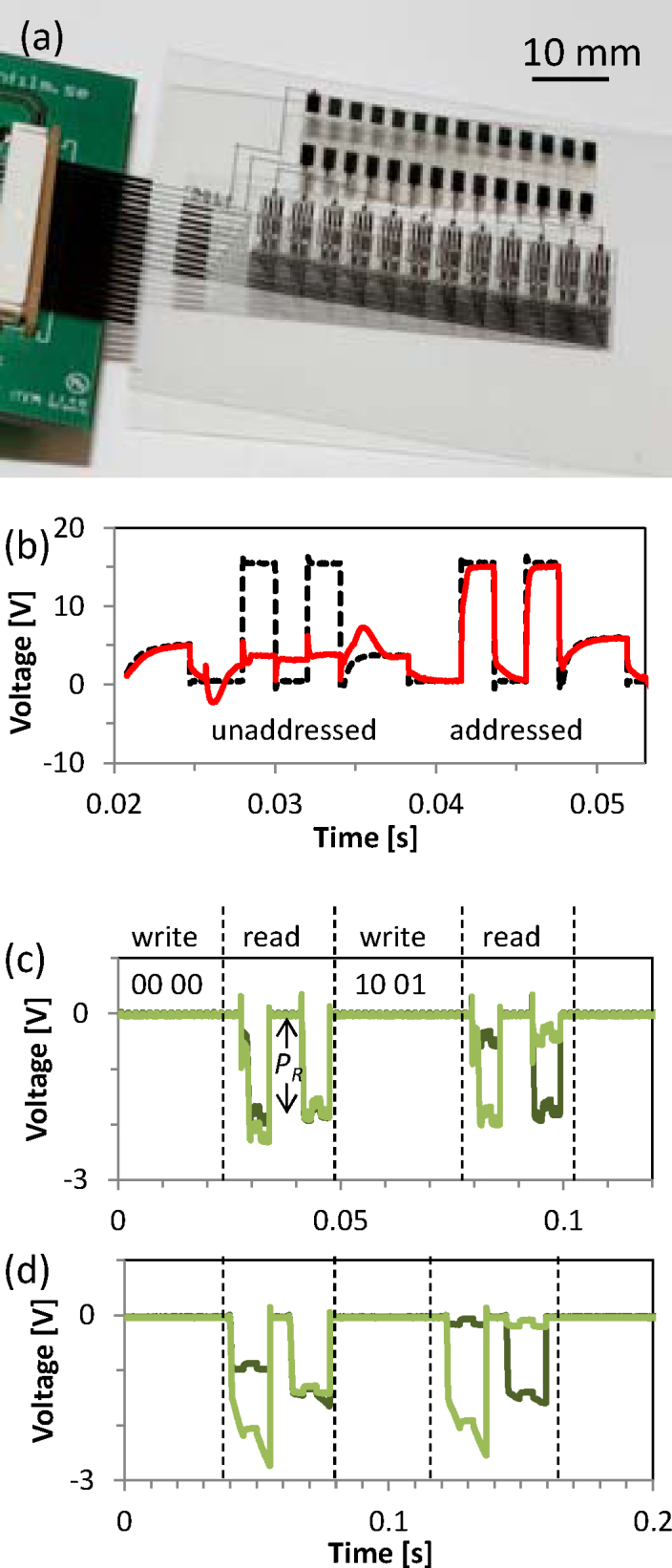
(a) Photograph of a 3-bit decoder circuit and ferroelectric capacitor memory. Four redundant sub-units were included in this photograph for yield improvement. (b) Input (black dotted line) and output (red line) signals through the printed decoder circuit. The output signal follows the input if the decoder sub-unit is addressed, whereas the output signal is floating when the sub-unit is un-addressed. (c) Bit-line signals read from a 2×2 array of memory capacitors patterned by photolithography. The two lines with different shades of green represent two neighboring bit-lines. Remnant polarization PR is indicated by the black arrow. (d) Same as (c) but the memory capacitors were patterned by gravure printing.
The decoder is further tested in combination with ferroelectric memory cells. In two tests, the decoder unit outputs are connected to the word lines of photolithographically patterned and gravure printed memory arrays. The latter combination represents an all-additively fabricated circuit. The combined units are tested by writing values to cells on multiple word lines and bit lines, then reading all the values. In these tests, the word-line and bit-line waveform generation, memory address signal generation, and charge integration are external to the decoder circuitry.
Figure 6(c) shows the decoder addressing a photolithographically-patterned memory array. The dark green and light green signals are measured at two neighboring bit lines. Successful writing and reading of four cells on a 2×2 sub-array is sufficient to verify decoder functionality and scalability. The four cells are set to the 0 state by addressing the word lines sequentially and transmitting the appropriated word-line and bit-line waveforms as in Fig. 5. The cells are then read in pairs by the two bit-line integrators as the word lines are successively addressed. The large amount of charge recorded by the integrators indicates the correct polarization (all 0 states) is obtained from all four cells. The double-pulse read scheme used helps provide a reference to compensate for slight variations in memory cell size. In the second half of the test sequence, the first word line is addressed and the state 10 is written to the two bit lines. Then the second word line is addressed and the state 01 is written. These four cells are subsequently read and all show the correct states. This test sequence indicates that each memory cell is properly addressed and is not disturbed by writing and reading of neighboring cells.
The fastest timing achieved with this decoder-memory unit is 5 ms write time with 2 ms setup time. The switching time is in agreement with the simulation results of <2.6 ms. The decoder output level changes less than 3% over a hundred successive repeats of the write-read sequences, with negligible change in slew rates within measurement error. This result verifies that the complementary circuit is stable against bias stress under these conditions.
The above write and read sequences are also applied to gravure-printed memory cells, with the results shown in Fig. 6(d). Here, again, the written values are clearly retained and successfully read, although there is a slight drift in output voltage over the 5 ms read period due to memory cell leakage.
Discussion
A flexible electronic system with organic memory and logic circuits is achieved by additive printing, and this is designed with tolerance to the device variations and instability found in print manufacturing. The decoder described here enables the scalability of printed memory, which is essential to future applications with sensor networks, smart tags and packaging, and numerous other applications. Moreover, the decoder circuit is applicable to addressing other types of arrays often used in large-area electronic applications. The circuit design techniques and device performance guidelines here are generally applicable to other organic circuits. These methodologies will enable design toolkits, ultimately leading towards the realization of manufacturable printed electronics.
Methods
A. Fabrication process
Circuits are fabricated on a mechanically flexible substrate cut from 125-μm polyethylene naphthalate (PEN) film (Dupont Teijin). Electrode contacts are fabricated by inkjet-printing a silver-nanoparticle solution (Cabot)30. The source/drain electrodes for p-channel transistors are treated with tetrafluoro-tetracyanoquinodimethane (F4TCNQ, 0.5% by weight in dichlorobenzene)31 to reduce contact resistance. There is no contact treatment for the n-channel transistors. Channel lengths of 35 μm are used in the circuit design, and channel widths are as in Fig. 3(a). The semiconductors are inkjet-deposited over transistor channels, and a 400-nm-thick fluoropolymer dielectric is coated and shows a capacitance of Cg = 5 nF/cm2. Vias between the source-drain layer and the gate layer are made by laser ablation of the dielectric and via connections are made by printing Ag.
The memory elements are capacitors with a ferroelectric poly(vinylidene fluoride)-based copolymer as the dielectric. The co-polymer is deposited between top and bottom metal lines that arranged perpendicular to each other such that the memory capacitors are formed at intersections of the electrodes. The memory cells are fabricated with the metal electrodes patterned by either gravure printing on PET substrates or photolithographic processing on PEN substrates. For the gravure-printed cells, the electrodes are Ag with bottom electrode line widths of 240 μm and top electrode line widths of 135 μm, corresponding to a capacitor area of 240 × 135 μm2. The photolithographically defined electrodes were Au, with a capacitor area of 50 × 50 μm2. The complete decoder and the memory structures are electrically connected by printing Ag lines.
B. Measurement method
All electrical measurements are performed at room temperature and in air. Custom external circuitry and software provides decoder address signals as well as word-line and bit-line waveforms. Custom high-impedance active probes are used for measurement of internal node voltages. The external circuit also includes charge integrators for readout.
Author Contributions
T. N. N., D. E. S., P. B. designed and coordinated the experiments. J. V. and C. K. were project supervisors. T. N. N., D. E. S., L. L. L., G. L. W., B. R., B. K., P. B., L. H., N. A., O. H., J. N. performed experiments. T. N. N., D. E. S., L. L. L., G. L. W., J. V., P. B., L. H, N. A., O. H., J. N., C. K. analyzed data. T. N. N. and D. E. S. wrote the paper, with editing contributions from all the co-authors.
Acknowledgments
We are grateful to Antonio Facchetti and Xia Yu for providing Polyera materials. We thank A. C. Arias for fruitful discussions.
References
- Weiser M. Hot topic: Ubiquitous computing. IEEE Computer, Oct, 71–72 (1993). [Google Scholar]
- Berggren M. & Richter Dahlfors A. Organic bioelectronics.. Adv. Mater. 19, 3201–3213 (2007). [Google Scholar]
- Loo Y. L. et al. Soft, conformable electrical contacts for organic transistors: high resolution circuits by lamination. Proc. Nat. Acad. Sci. U.S.A. 99, 3327–3334 (2002). [DOI] [PMC free article] [PubMed] [Google Scholar]
- Ng T. N., Wong W. S., Lujan R. & Street R. A. Characterization of charge collection in photodiodes under mechanical strain: comparison between organic bulk heterojunction and amorphous silicon. Adv. Mater. 21, 1855–1859 (2009). [Google Scholar]
- Ishida K. et al. Stretchable EMI measurement sheet with 8×8 coil array, 2 V organic CMOS decoder, and 0.18 um silicon CMOS LSIs for electric and magnetic field detection. IEEE J. Solid-State Circuits 45, 249–259 (2010). [Google Scholar]
- Sekitani T., Noguchi Y., Zschieschang U., Klauk H. & Someya T. Organic transistors manufactured using inkjet technology with subfemtoliter accuracy. Proc. Nat. Acad. Sci. U.S.A. 105, 4976–4980 (2008). [DOI] [PMC free article] [PubMed] [Google Scholar]
- Arias A. C., MacKenzie J. D., McCulloch I., Rivnay J. & Salleo A. Materials and applications for large area electronics: solution-based approaches. Chem. Rev. 110, 3–24 (2010). [DOI] [PubMed] [Google Scholar]
- Yan H. et al. A high-mobility electron-transporting polymer for printed transistors. Nature 457, 679–686 (2009). [DOI] [PubMed] [Google Scholar]
- Minemawari H. et al. Inkjet printing of single-crystal films. Nature 475, 364–367 (2011). [DOI] [PubMed] [Google Scholar]
- Xiong W., Zschieschang U., Klauk H. & Murmann B. A 3V 6b successive-approximation ADC using complementary organic thin-film transistors on glass. ISSCC Dig. Tech. Papers 134–135 (2010). [Google Scholar]
- Myny K. et al. P., An 8b organic microprocessor on plastic foil. ISSCC Dig. Tech. Papers 322–324 (2011). [Google Scholar]
- Daami A. et al. Fully Printed Organic CMOS Technology on Plastic Substrates for Digital and Analog Applications. ISSCC Dig. Tech. Papers 328–329 (2011). [Google Scholar]
- Ng T. N., Russo B. & Arias A. C. Solution-processed memristive junctions used in a threshold indicator. IEEE Trans. Electron Dev. 58, 3435–3443 (2011). [Google Scholar]
- Jung M. et al. All-printed and roll-to-roll-printable 13.56-MHz-operated 1-bit RF tag on plastic foils. IEEE Trans. Electron Dev. 57, 571–580 (2010). [Google Scholar]
- Sekitani T. et al. Organic non-volatile memory transistors for flexible sensor arrays. Science 326, 1516–1519 (2009). [DOI] [PubMed] [Google Scholar]
- Naber R. C., Asadi K., Blom P. W. M., de Leeuw D. M. & de Boer B. Organic non-volatile memory devices based on ferroelectricity. Adv. Mater. 22, 933–945 (2010). [DOI] [PubMed] [Google Scholar]
- Ng T. N., Russo B., Krusor B., Kist R. & Arias A. C. Organic inkjet-patterned memory array based on ferroelectric field-effect transistors. Org. Electron. 12, 2012–2018 (2011). [Google Scholar]
- Sirringhaus H. Reliability of organic field-effect transistors. Adv. Mat. 21, 3859–3873 (2009). [Google Scholar]
- Street R. A., Chabinyc M. L., Endicott F. & Ong B. Extended time bias stress effects in polymer transistors. .J. Appl. Phys 100, 114518 (2006). [Google Scholar]
- Ng T. N., Chabinyc M. L., Street R. A. & Salleo A. Bias stress effects in organic thin film transistors. IEEE International Reliability Physics Symposium Proc., Phoenix, 066101 (2007). [Google Scholar]
- Ng T. N. Russo B. & Arias A. C. Degradation mechanisms of organic ferroelectric field-effect transistor used as non-volatile memory. .J. Appl. Phys 106, 094504 (2009). [Google Scholar]
- Bode D. et al. Noise-margin analysis for organic thin-film complementary technology. IEEE Trans. Electron Dev. 57, 201–208 (2010). [Google Scholar]
- Ng T. N., et al. Electrical stability of inkjet-patterned organic complementary inverters measured in ambient conditions. Appl. Phys. Lett. 94 (2009) 233307. [Google Scholar]
- Myny K. et al. Robust digital design in organic electronics by dual-gate technology. ISSCC Dig. Tech. Papers 140–142 (2010). [Google Scholar]
- Huang T.-C. et al. Pseudo-CMOS: a design style for low-cost and robust flexible electronics. IEEE Trans. Electron Dev. 58, 141–150 (2011). [Google Scholar]
- Meixner R. et al. A physical-based PSPICE compact model for poly(3-hexylthiophene) organic field-effect transistors. IEEE Trans. Electron Dev. 55, 1776–1781 (2008). [Google Scholar]
- Bartzsch M., Kempa H., Otto M., Hübler A. & Zielke D. Device and circuit simulation of printed polymer electronics. Organic Electron. 8, 431–438 (2007). [Google Scholar]
- Heremans P. et al. Polymer and organic non-volatile memory devices. Chem. Mater. 23, 341–358 (2011). [Google Scholar]
- Sheikholeslami A. & Gulak P. G. A survey of circuit innovations in ferroelectric random-access memories. Proc. IEEE 88, 667–689 (2000). [Google Scholar]
- Daniel J. et al. Jet-printed active-matrix backplanes and electrophoretic displays. Jap. J. Appl. Phys. 46, 1363–1369 (2007). [Google Scholar]
- Whiting G. L. & Arias A. C. Chemically modified ink-jet printed silver electrodes for organic field-effect transistors. Appl. Phys. Lett. 95, 253302 (2009). [Google Scholar]


