

Abstract
We report the use of an array of electrically gated ~200 nm solid-state pores as nanofluidic transistors to manipulate the capture and passage of DNA. The devices are capable of reversibly altering the rate of DNA capture by over three orders of magnitude using sub-1V biasing of a gate electrode. This efficient gating originates from the counter-balance of electrophoresis and electroosmosis, as revealed by quantitative numerical simulations. Such a reversible electronically-tuneable biomolecular switch may be used to manipulate nucleic acid delivery in a fluidic circuit, and its development is an important first step towards active control of DNA motion through solid-state nanopores for sensing applications.
Keywords: nanopore, nanofluidic transistor, DNA capture, gate manipulation, biomolecular switch
Over the past 15 years nanopores have garnered significant interest as single-molecule analytical tools.1–4 Much of this interest has been motivated by DNA sequencing, where sub-10nm pores are used to confine the motion of nucleotides in a single-file, sequential order.2–8 More recently, researchers have investigated the capability of nanopore devices to manipulate ionic and biomolecular transport. In particular, establishment of a salt gradient between the two sides of the membrane has been used to enhance DNA capture;9 surface modification of a nanopore wall has been shown to significantly impact biomolecular translocation;10–12 electrowetting has been used to reversibly open and close hydrophobic nanopores;13 and gated nanopores have modulated ionic current14–19 and offered the prospect of greater control over molecular translocation.20–27 Among these approaches, the use of an active, embedded gate electrode is attractive due to its natural integration with electronic control, enabling precise, rapid feedback,28 in addition to offering alternative DNA sensing mechanisms.29–31
Thus far, the majority of the work involving control of biomolecular capture and transport, by an active embedded gate electrode, has been performed computationally,29, 32 while many experimental14, 15 and numerical16–19 investigations of electrically gated nanofluidic devices have remained limited to ionic transport control. Two previous studies have demonstrated control of molecular capture using a gate electrode, one in nanochannel devices21 and another in polycarbonate track-etched pores.22 In both cases, the observed modulations were modest (< 10-fold). Further, in the nanochannel case, extreme biasing conditions21 (ΔVG~100 V) were used, which are impractical for most biosensing applications and detrimental to the device integrity33, and in the track-etched pores, the underlying mechanism was not well explored.22
In this article, we report the use of electrically-gated ~200 nm pores as a reversible electronically-tuneable biomolecular switch. We demonstrate highly effective electrostatic control of the nucleic acid capture rate with > 1000-fold modulation using sub-1V gate biases. These devices were fabricated to exploit the barrier-limited operation arising from the balanced interplay between electroosmotic flow (EOF) and electrophoresis for pores of this size and aspect ratio.38 The method relies on varying the gate voltage to modulate the shape of the electric double layer (EDL) to finely tune the strength of the EOF opposing the DNA's electrophoretic motion. We have determined that operating these so-called nanofluidic transistors (NFT) within the sub- to near-threshold regime allows for exponential (or super-linear) control of the DNA capture rate. We present detailed numerical simulations to quantitatively elucidate the underlying mechanism of NFT operation and the effects of electrical biases, solution pHs, NFTs surface properties and NFT device dimensions.
Results and Discussion
Device Fabrication
We fabricated NFT devices, which consist of a 4×4 array of pores in a SiNx membrane, covered on one side by a sputtered Au film, and coated with conformal Al2O3 by atomic layer deposition (ALD). Two versions of the NFT were fabricated, a thick version with 140 nm thick membranes and ca. 200 nm pores and a thin version with 80 nm thick membranes and ca. 160 nm pores. This aspect ratio allows for our devices to operate in a barrier-limited regime, in addition to relaxing their fabrication constraints.2, 32, 33 Figure 1 shows schematic drawings of the NFTs, where DNA molecules flow from the source reservoir into the drain reservoir, and a scanning electron microscopy (SEM) image of one of the pore arrays used. We fabricated arrays of 4×4 pores rather than a single pore to increase the molecular flux, mainly for the purpose of quantitative polymerase chain reaction (qPCR) used to quantify the amount of DNA captured and translocated, see qPCR Based Capture Rate Metrology in the Methods section.
Figure 1.

Schematics and SEM image of the nanofluidic transistor. a) The NFT is in buffered 10 mM NaCl solution. The source well is grounded through an Au or an Ag/AgCl electrode, and contains 2.5 nM of 100bp DNA fragments. The drain well has +800 mV applied through an Au or an Ag/AgCl electrode. b) Two versions of the NFT were made, thick and thin. The thick NFT is designed to have a 140 nm thick membrane composed of 30nm thick SiNx and 80nm of gate material surrounded by 15 nm of Al2O3 deposited by ALD. The thin NFT has an 80 nm thick membrane composed 10 nm thick SiNx and 50 nm of gate material surrounded by10 nm Al2O3. c) The pores are milled by FIB 500 nm apart in a 4×4 square pattern. d) SEM image of an array. The scale bar is 500 nm long.
The thick NFT devices were fabricated from 50 × 50 μm, 30 nm thick free-standing SiNx membranes (SPI part#4104SN-BA and Norcada part#NT005X) supported on a 200 m thick silicon frame. We deposited, on the SiNx side, a 75 nm thick Au film on top of a 5 nm thick Cr adhesion layer by sputtering to serve as the gate electrode. A 4×4 array of pores, with diameter ca. 200 nm, is milled by focused ion beam (FIB, FEI Strata 235DB). We then deposit 15 nm of Al2O3 by ALD to insulate the gate, and prevent direct leakage currents.34 Total thickness was targeted to be 140 nm; however, chip-to-chip process variation resulted in some of the NFT being slightly thinner (as thin as 130 nm). DNA capture rate modulation experiments were first performed with these “140 nm” or thick NFT. We fabricated a second version of the NFT to investigate the effect of the pore and membrane dimensions and gate oxide thickness on the device's ability to modulate DNA capture rate. To that end, we sputtered 45nm of Au (with additional 5 nm Cr adhesion layer) on 10 nm SiNx membranes (Norcada part#NT005Z). Using a shadow mask, an additional 100 nm of Au was deposited on one of the corners of these chips to serve as a bond pad. A 4×4 array of pores, with diameter ca. 160 nm, was milled by FIB. We then deposited 10 nm of Al2O3 by ALD to insulate the gate, for a total device thickness of 80 nm. In subsequent sections of this article, the “80 nm” NFT will be referred to as the thin NFT, while the “140 nm” NFT will be referred to as the thick NFT.
The NFTs are mounted onto printed circuit boards (PCBs) to make electrical contact to the gate electrode and are immersed into liquids in polytetrafluoroethylene (PTFE) cells that form the source and drain reservoirs, see Protocols and Instrumentation in the Methods section. A compact-battery-powered-custom-built instrument is used to apply voltages and measure the current at each electrode (drain, gate, source), see Supplementary Figure S1. The instrument has three independent current amplifiers on a PCB housed in a copper Faraday cage. The instrument is controlled by a National Instruments data acquisition card through a LabView virtual instrument in a personal computer.
DNA Capture Rate Modulation
During our experiments, we fixed the drain voltage, VD, at +800 mV and varied the gate voltage, VG, between 0 V and +500 mV. Multiple gate voltage sweeps, from low VG to high VG, are made for each device, in order to confirm the reproducibility of the gate control. DNA flows from the source well into the drain well. Two Au or Ag/AgCl electrodes are used to apply a bias between the drain and the source. The wells are filled with buffered 10 mM NaCl solutions. At the start of the experiments, DNA is injected into the source well setting the concentration at 2.5 nM. Following application of electrical biases at the drain and gate electrodes, three timed samples from the drain well are taken at 10 minute intervals.
DNA capture rates versus VG for thick NFT devices at various pH values are shown in Figure 2a and b. The data points are the averages of the measured capture rates for each experimental condition and the error bars are the standard deviations. The solid lines are the capture rates determined from the device level simulations; parameters used are listed in Supplementary Tables S2 and S3. The source/drain electrodes are Au for the thick devices. The gate voltage on the thick devices reversibly modulates the DNA capture rate by ca. 10× with sub-1V gate bias. For pH 9.2, the increase from 390/s to 3800/s is seen for a ΔVG of 250 mV. For pH 9.6, an increase from 520/s to 5300/s is seen for a ΔVG of 400 mV. For pH 10.5, an increase from 300/s to 2600/s is observed for a ΔVG of 300 mV. This control is super-linear vs. VG, as expected from a barrier-limited operation that is fully discussed later. Given a gate bias (VG), the capture rate decreases with increasing pH. Thus, by adjusting the pH one can tune the threshold voltage on VG, beyond which the NFT switches on to allow biomolecule translocation. Further, fixing VD = 0 V while varying VG, shows that the diffusive translocation rate of DNA is small, ca. 50/s, ruling out diffusion as the primary transport mechanism. The simulation also predicts an un-modulated diffusive translocation rate of 40/s in this control case.
Figure 2.
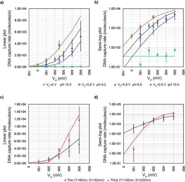
Experimental results of DNA capture rate vs. VG compared to simulation. The markers represent the experimental results. The error bars are standard deviations of experimental results. Simulated results are shown in solid lines. a) The plot of DNA capture rate vs. VG for various solution pHs of the thick NFT devices. When VD = +800 mV, VG is able to control DNA capture rate of the nanofluidic transistor (NFT) by altering the counter ion concentration. Further, the solution pH also alters pore surface charge. Thus, changing pH result in shifting the DNA capture threshold. In simulations, this pH dependence is modeled by assigning different surface charge densities (Supplementary Information Table S3). We also performed the experiment when VD = 0 V, the net translocation rate is small, ca. 50/s. b) The semi-log plot of the results shown in Figure 2a. c) The plot of DNA capture rate vs. VG of NFTs before and after the design revision to enhance modulation. Both devices are in solution with pH 9.6. The thin device, with smaller diameter pores and a thinner gate dielectric film, has enhanced gate control. The application of same VD across a thinner membrane results in larger trans-membrane electric field as well. This results in stronger relative EOF that can turn the device off at low VG and have larger capture rate at high VG. d) The semi-log plot of the results shown in Figure 2c.
In an effort to further enhance biomolecular capture modulation, the gate control is increased by employing the thin NFT, where the membrane thickness is reduced from 140 nm to 80 nm, the pore diameter from 220 nm to 160 nm and the gate oxide thickness from 15 nm to 10 nm (Figure 1b). Due to the over potential of Au source/drain electrodes used for the thick NFTs, we found that the measured ionic current for the thick NFT was depressed compared to measurements performed with Ag/AgCl electrodes; though this does not appear to hinder the DNA capture rate modulation. Nevertheless, for the thin NFT, we used ideally non-polarizable Ag/AgCl electrodes instead to more accurately monitor the ionic current through the pores. At pH 9.6, the thick devices show capture rate modulation from 520/s when VG = +100 mV to 5300/s when VG = +500 mV, whereas the thin NFT's range from 2.5/s to 12000/s under the same conditions, a 4000× modulation, as illustrated in Figure 2c and d. Not only does the thin NFT provide improved modulation amplitude, but it also offers superior shut off state for biomolecular passage at low VG.
As the number of molecules present in the drain well is used to compute the translocation rate, DNA molecules from one experiment must be removed prior to performing the next experiment. We have found that unmounting NFT devices from the PTFE cells for cleaning resulted in too many devices being damaged. We therefore simply perfuse fresh, buffered electrolyte solutions in each well regularly, until acceptable background levels for qPCR experiments are reached. This cleaning process can take several days. This slow reset of the NFT devices implies that a VG sweep may take up to two weeks. Since each device survived at least two VG sweeps, most devices endured at least a few weeks of experiments. We confirmed the stability of the NFTs during this time, and under the experimental conditions, by recording ionic current at the drain, and source electrodes, while also monitoring leakage at the gate electrode to ascertain integrity of the Al2O3 gate oxide coating.35
Device Conductance & Gate Leakage Currents
In order to analyze device operation and monitor the condition of the gate electrode, we simultaneously measured currents at all three electrodes. After being immersed in buffered 10 mM NaCl, each 4×4 array of pores was characterized to check for linear current-voltage (I-V) characteristics, conductance stability and noise. We recorded currents at 10 kHz sampling frequency and the signals were software filtered at 1 kHz. For large pores, in low salt concentrations, we estimated the conductance based on geometrical factors36 (approximating the actual pore shapes as cylinders and taking access resistance into account) and the surface charge, see Conductance Calculations in the Supplementary Information. Under these approximations the conductance, G, can be calculated with the following expression:
| (1) |
where d is the diameter of the pore, l is the thickness of the membrane, μ+ is the mobility of the counter ion, ρ is the surface charge density and σ is the bulk conductivity. This formula gives an estimated conductance of ca. 30 nS for a single pore, or 480 nS for the array of the thin NFT. This is in reasonable agreement with the experimental value of ~550 nS, considering the simplification of the model, not accounting for secondary geometric effects or the presence of the gate electrode which causes local redistributions of ions inside the pores. We verify conductance stability of all of our devices before and after DNA capture experiments. Although we have witnessed some variations in conductance during the operation of our NFTs, we only included data for devices showing ionic current deviation < 10% for a given set of VD and VG. Interestingly, we have observed reproducible modulation in the ionic current in some of our NFTs, see Supplementary Figure S3. In particular, the thin devices revealed significant modulation in the ionic current. The basis for this effect16, 17 is the subject of on-going research and is outside the scope of this work.
Although a thin layer of Al2O3 surrounds the gate electrode, the gate leaks a small amount of current to the source and the drain.33 Figure 3a shows the gate leakage current recorded for the various NFTs used. The time-averaged drain and source ionic currents during the DNA capture rate modulation experiments are shown in Supplementary Figure S3. The choice of VG range, to ensure low gate leakage current, also keeps the leakage current's effect from dominating the behavior of the NFT.34 Figure 3b shows the contribution of the gate leakage to the NFT ionic currents. The choice of VG used is near the minima. The current-time traces at the drain and the gate electrodes of the thin device are show in the Supplementary Figure S4.
Figure 3.

Average currents during the DNA translocation experiments. Error bars are RMS noise of the currents measured. a) The gate leakage currents (IG) as functions of the applied gate bias (VG). b) The magnitude ratio of the gate leakage current (IG) to the drain ionic current (ID).
We set VD=+800 mV in all of our DNA capture rate experiments to maximize the translocation rates, for the purpose of qPCR analysis, while at the same time keeping the integrity of the devices. It has been experimentally observed that the application of VD=+1 V resulted in very high gate leakage current (> 100nA) which irreversibly damaged the gate electrode, see Supplementary Figure S5.
Analysis of NFT Operation
Detailed numerical simulations have been developed to quantitatively model the device operation, where the electrostatics and the transport of DNAs, cations/anions and fluids have been fully accounted for. The DNA movement is modeled by the Smoluchowski equation:
| (2) |
where is the DNA flux, CDNA is the DNA concentration, D is the DNA diffusion coefficient, μ is the DNA electrophoretic mobility, ψ is the electrostatic potential and is the fluid velocity. The flux is usually dominated by DNA electrophoresis, CDNAμ▽ψ, and advection, , while diffusion, - D▽CDNA, plays an insignificant role as demonstrated in our experiments and simulations. Since the external pressures that drive our system are negligible, the advection process is determined by the electroosmotic flow (EOF). In the past, the Poisson-Nernst-Plank (PNP) and the Stokes equations were self consistently solved using a modified version of the general purpose device simulator PROPHET.16, 17 In this work we extend the previous work by using the solution to the PNP and Stokes equations to solve the full Smoluchowski equation for DNA transport.
The solution of Smoluchowski equations, Eq. (2), requires the profiles of ψ and as input. For this purpose, the Poisson-Nernst-Planck (PNP) and Stokes equations are self-consistently solved first for ψ, , and and the concentrations of cations (C+) and anions (C−). The PNP equations are
| (3) |
where εW is the dielectric constant of the solution, q the elementary charge, D± and μ± the diffusion coefficients and mobilities of cations and anions, respectively. The fluid transport is modeled by the Stokes-divergence equations
| (4) |
where p is the solvent pressure γ and is the solvent viscosity.
By analyzing the simulation results we elucidate the mechanism of device operation. For salt solutions with pH > 9.1, the Al2O3, gate oxide bears a negative surface charge37, which makes the direction of DNA electrophoresis and EOF oppose one another. The interaction between these two fundamental processes has been previously studied23 and employed for DNA aggregation in nanodevices.24–26 At low VG, the gate enhances Na+ concentration near the pore walls, which results in a strong EOF opposing DNA entry into the pore. Figure 4a illustrates this phenomenon graphically. Despite the strong external electric field acting on the DNA molecules, EOF is rejecting DNA from the pore, preventing molecular capture. Figure 4d shows the simulated components of vertical DNA velocities, where at all points along the pore entrance EOF is greater than electrophoresis. At high VG, the electrostatic effect of the gate reduces Na+ concentration near the pore walls. Figure 4b illustrates the dynamics when VG is high. The strength of EOF is now lowered below the constant electrophoretic force acting on DNA molecules, enabling DNA captured by the pore. Figure 4e shows the plot of simulated components of vertical DNA velocities when VG is high. Unlike the low VG case, electrophoretic DNA movement is observed to exceed EOF at the perimeter of the pore. The efficient control of DNA capture rate is made possible by operating the NFT in a barrier-limited regime which has previously been studied in detail.38 Operating the device immediately above or below a certain threshold value of VG, one can obtain exponential (in sub-threshold), super-linear (near-threshold) or linear (above-threshold) control over DNA capture rate. Having the EOF much stronger than electrophoresis can reduce the DNA capture exponentially, and having the EOF much weaker than electrophoresis can enhance the DNA capture linearly. Given our choice of pore dimensions, the NFTs operate in sub-threshold to near threshold regime, where a small change in the EOF results in significant modulation of DNA capture rate.
Figure 4.

Schematic of the EOF barrier limited operation. a) The schematic of the barrier-limited operation when VG is low. The gate attracts Na+ ions to the pore wall. The resulting EOF is stronger than electrophoresis (EP); hence NFT rejects DNA from entering the pore. b) When VG is high, the gate reduces Na+ ion concentration on the pore wall. This weakens EOF, allowing the pore to accept DNA for capture. c) The locations where the one dimensional plots in d, e and f of this Figure are made. d) The simulated components of vertical DNA speed. In regions where EOF speed exceeds electrophoretic DNA speed, the pore will reject DNA from entering it. When VG is low, the rejecting region covers most of the pore entrance. The pore is 200nm in diameter. e) When VG is high, the reduction in EOF speed results in a retreat of the rejecting region, and some portions of the pore open up for DNA capture. f) The electrophoretic DNA speed peaks at the vertical center of the pore. The EOF speed peaks further out the pore in the source side. The difference in the peak locations of EOF and electrophoresis results in a region at the source that rejects DNA from being injected into the pore.
One notes that the EOF profiles in Figure 4d and e do not fully develop into the classical profile. EOF was found to take ca. 10 ns to fully develop into its classical profile in a 200 nm wide channel.39 Since the expected transit time of fluid through the pore is ca. 1 ns, its profile is not fully developed through the short channel. It is interesting to observe that the electric field strength peaks mid way through the pore length while EOF peaks near the pore entrance. This shift between the EOF and electrophoresis peaks, reveals a region where strong EOF prevents DNA transport across the pore, see Figure 4f.
Further observations about local DNA concentration give insights into the translocation path of DNA molecules. As shown in left hand side of Figure 5a, the strong EOF at low VG, pushes the DNA away from the pore entrance. For the VG=+500 mV case shown in right hand side of Figure 5a, the EOF barrier retreats due to high VG, and the reduced barrier opens the perimeter of the pore to allow DNA to be captured. The shape of the barrier is visualized by looking at the region where DNA is being pushed away from the pore, as shown by the driving force plot in left hand side of Figure 5b for the VG =+100 mV case. A plug shaped barrier is located at the pore entrance, and controls the DNA injection into the pore. In this case, the device is off, and the plug-shape barrier fits tightly over the pore, severely limiting the capture rate and the translocation velocity. When the device is on, in the VG=+500 mV case on the right hand side of Figure 5b, the barrier shrinks in dimension and magnitude and an opening at the perimeter of the pore is created to allow DNA capture. Because the NFT's pores diameter is ca. 200 nm, the translocation kinetics of 100bp fragments cannot be directly measured by ionic current recording. However, we can speculate based on the simulation results, that the complex dynamics created by the interplay of EOF and electrophoresis, seen in Figure 5b, will cause a widening of the distribution of translocation speeds. Some DNA molecules will translocate with moderate speeds while others will be held near the border between the barrier and the opening seen in Figure 5b. This also results in the local DNA concentration enhancements near the entrance of the pore seen in Figure 5a.
Figure 5.

Simulation results: DNA concentration and driving force. a) The pore diameter is 200 nm and the membrane thickness is 140 nm. The NaCl solution pH is 9.6. When VG is low at +100 mV (left), advection by electro-osmotic flow (EOF) rejects DNA from entering. When VG is high at +500 mV (right), the EOF decreases and DNA is captured by the pore for translocation. b) The regions with positive values represent those areas where DNA is being pushed away from entering the device. When VG is +100 mV (left), the strong EOF results in a large region where DNA is moving away from the pore, nearly all of the pore entrance on the source side is covered with this blocking region. When VG is +500 mV (right), reduced EOF allows more DNA to be captured, the blocking region is physically smaller than the VG = +100 mV case. The capture process occurs at the perimeter of the pore. This is due to the viscous fluid flow maintaining its profile further into the source well than the more rapidly dispersing electric field.
Lastly, we note that the threshold behavior observed in our NFTs could potentially enable the selective capture of biomolecules based on their free-solution electrophoretic mobility or by the use of drag tags.40 According to Eq. (2) and the fact that the diffusion only plays a negligible role, the capture of biomolecules by the NFTs is primarily mobility-dependent. Such a characteristic could be used to purify biomolecules in lab-on-a-chip devices.
Conclusion
By adjusting the NFTs dimensions, its surface property, the salt concentration and the pH, the interplay between the EOF and DNA electrophoresis is varied. As revealed by detailed numerical simulations, the counter-balance of these opposing flows is key to the operation of the device. The resultant barrier-limited operation enables our NFTs to control the rate of capture of DNA by over three orders of magnitude with a sub-1V bias applied to an embedded metal gate. The solution pH is also shown to tune the threshold voltage. We envision such NFT devices as an electrically-active component of fluidic circuitry to reversibly manipulate biomolecule delivery to a downstream sensor or to purify biomolecules based on their free solution mobility.
Methods
Buffered Solutions
The 10mM NaCl solutions used are buffered with 10 mM of buffering agents AMPSO or CAPS. The buffer AMPSO has useful range of pH 8.9 ~ pH 9.7 and the buffer CAPS has useful range of pH 9.7 ~ pH 11.1. The pH is adjusted with NaOH. Three solutions are prepared at pH 9.2, pH 9.6 and pH 10.5. The solution at pH 9.2 contains 10 mM NaCl and 10 mM AMPSO. The solution at pH 9.6 contains 10 mM NaCl, 10 mM AMPSO and sufficient amount of 1 M NaOH is added to alter the pH to 9.6. The solution at pH 10.5 contains 10 mM NaCl and 10 mM CAPS.
Protocols and Instrumentation
The NTF chips were submitted to the following cleaning procedure: 10 min in acetone, followed by immersion in methanol, and isopropanol. The NFTs are then mounted onto printed circuit boards (PCBs) to make electrical contact with the gate electrode. Polydimethylsiloxane (PDMS) is used to seal the NFT chips onto a printed circuit board (PCB). Electrical contact to the gate electrode is made through a wirebond, which is insulated with PDMS. Immediately prior to immersing into liquids, the PCB mounted NFT chips undergo a 60 s, 18 W plasma treatment (Harrick Plasma PDC-32G), to render the pore surface hydrophilic and facilitate wetting. The PCB is then clamped between two polytetrafluoroethylene (PTFE) half-cells with custom-made silicone gaskets to form a fluid tight seal, between the source and drain reservoirs. The reservoirs (1 mL each) are filled with filtered, degassed and buffered liquid electrolyte at room temperature. The cell is placed in a Faraday enclosure to reduce electrical noise. Au or Ag/AgCl electrodes immersed in each reservoir were used to apply voltages and measure ionic current when connected to a current amplifier. A custom-designed transimpedance amplifier was used to record ionic current at 10 kHz sampling frequency, and to perform I-V characterization and DNA capture experiments. Data acquisition was performed using custom-designed LabVIEW software controlling a National Instruments PCI-6120 or USB-6351 DAQ card. Supplementary Figure S1 shows photographs of the instrument and a NFT mounted on the PTFE cells.
Preparation of Test DNA
For our capture experiments, we used a 100bp fragment of λ DNA. To generate sufficient copies of the fragment, we performed PCR to duplicate the fragment from stock λ DNA. We used the following primers, ordered from Integrated DNA Technologies (IDT): forward primer, 5'-GCAAGTATCGTTTCCACCGT-3' and reverse primer, 5'-TTATAAGTCTAATGAAGACAAATCCC-3'. The following reagents were used for each polymerase chain reaction (PCR) with a final volume of 50 μL: 10× PCR buffer (5 μL), dNTP (1 μL), 10 μM forward primer (1 μL), 10 μM reverse primer (1 μL), 25 mM MgCl (5 μL), Taq DNA Polymerase (1 μL), 25 ng/μL λ DNA (0.5 μL), and deionized (DI) water (35.5 μL). The Taq DNA Polymerase, 10× PCR buffer, dNTP and λ DNA were purchased from New England Biolabs (Part numbers M0273L, N0447L, and N3011S). The mixed reagents goes through the following thermal cycle: 1 cycle for 600 s at 95 °C, followed by 40 cycles of 30 s at 95 °C for denaturation, 30 s at 60 °C for annealing and 30 s at 72 °C for extension. The PCR product is purified using the QIAquick PCR Purification Kit (250) (Qiagen part number 28106) following the PCR purification spin protocol. Rather than using the elusion buffer provided in the kit, the buffered 10 mM NaCl prepared for the experiment is used to elude the DNA off the QIAquick column.
qPCR Based Capture Rate Metrology
The timed aliquots taken from the drain well are analyzed by quantitative polymerase chain reaction (qPCR) to quantify the amount of translocated molecules, which is then used for the capture rate calculation. Each qPCR were carried out with a final volume of 10 μL consisting of 5 μL of SYBR® Green PCR Master Mix (Applied Biosystems part number 4385616), 2 μL of 2.5 mM primer mix (the primers are described in the 100bp test DNA preparation), 1 μL of DI water, and 2 μL of a timed sample from the drain well. The qPCR goes through the thermal cycle: 1 cycle for 600 s at 95 °C, followed by 40 cycles of 30 s at 95 °C for denaturation and 30 s at 60 °C for annealing.
Given the relatively large size of our source and drain reservoirs (~mL), we required a sufficiently high number of DNA molecules to translocate during the time of an experiments. The 4×4 array (16 pores) was chosen in part to allow sufficient DNA capture for this metrology. No Template Control qPCR runs had average CT of 31.5 or 5 molecules in each qPCR volume. Further, due to the time needed to clear DNA molecules from the drain reservoir in between experiments, each data point in Figure 2 represents DNA capture rates of multiple experiments done on the NFTs up to two weeks apart. Thus, the control of DNA capture rate by the NFT is reproducible to the error rate shown.
Supplementary Material
Acknowledgements
The authors thank J. Oh, H. Persson and U. Schlecht for invaluable help in setting up the biological and chemical aspects of the experiment. We thank C. Gupta for discussion in matters electro chemical. We thank H. Ran, P. Au, J. Thibert-Leduc and H. Kwok for the efforts they invested in aiding the experiments, fabrication of the instruments and analysis. This work was supported by National Institutes of Health (NIH P01 HG0000205), Defense Advanced Research Projects Agency (DARPA-N66001-09-1-2132), and Natural Sciences and Engineering Research Council of Canada.
Footnotes
Supporting Information Paragraph
A catalog of NFTs used in our experiments, a description of the instrument, further details of qPCR based metrology, conductance calculations, additional graphs of measured ionic currents and parameters used for the simulation can be found in the Supplementary Information. This material is available free of charge via the Internet at http://pubs.acs.org
References
- 1.Dekker C. Solid-State Nanopores. Nat. Nanotechnol. 2007;2:209–215. doi: 10.1038/nnano.2007.27. [DOI] [PubMed] [Google Scholar]
- 2.Branton D, Deamer DW, Marziali A, Bayley H, Benner SA, Butler T, Di Ventra M, Garaj S, Hibbs A, Huang XH, et al. The Potential and Challenges of Nanopore Sequencing. Nat. Biotechnol. 2008;26:1146–1153. doi: 10.1038/nbt.1495. [DOI] [PMC free article] [PubMed] [Google Scholar]
- 3.Venkatesan BM, Bashir R. Nanopore Sensors for Nucleic Acid Analysis. Nat. Nanotechnol. 2011;6:615–624. doi: 10.1038/nnano.2011.129. [DOI] [PubMed] [Google Scholar]
- 4.Nakane JJ, Akeson M, Marziali A. Nanopore Sensors for Nucleic Acid Analysis. J. Phys.: Condens. Matter. 2003;15:R1365–R1393. [Google Scholar]
- 5.Tabard-Cossa V, Wiggin M, Trivedi D, Jetha NN, Dwyer JR, Marziali A. Single-Molecule Bonds Characterized by Solid-State Nanopore Force Spectroscopy. ACS Nano. 2009;3:3009–3014. doi: 10.1021/nn900713a. [DOI] [PMC free article] [PubMed] [Google Scholar]
- 6.Venkatesan BM, Estrada D, Banerjee S, Jin XZ, Dorgan VE, Bae MH, Aluru NR, Pop E, Bashir R. Stacked Graphene-Al2O3 Nanopore Sensors for Sensitive Detection of DNA and DNA-Protein Complexes. ACS Nano. 2012;6:441–450. doi: 10.1021/nn203769e. [DOI] [PMC free article] [PubMed] [Google Scholar]
- 7.Garaj S, Hubbard W, Reina A, Kong J, Branton D, Golovchenko JA. Graphene as a Subnanometre Trans-Electrode Membrane. Nature. 2010;467:190–194. doi: 10.1038/nature09379. [DOI] [PMC free article] [PubMed] [Google Scholar]
- 8.Sadki ES, Garaj S, Vlassarev D, Golovchenko JA, Branton D. Embedding a Carbon Nanotube across the Diameter of a Solid State Nanopore. J. Vac. Sci. Technol. B. 2011;29:053001. [Google Scholar]
- 9.Wanunu M, Morrison W, Rabin Y, Grosberg AY, Meller A. Electrostatic Focusing of Unlabelled DNA into Nanoscale Pores Using a Salt Gradient. Nat. Nanotechnol. 2010;5:160–165. doi: 10.1038/nnano.2009.379. [DOI] [PMC free article] [PubMed] [Google Scholar]
- 10.Chun KY, Stroeve P. Protein Transport in Nanoporous Membranes Modified with Self-Assembled Monolayers of Functionalized Thiols. Langmuir. 2002;18:4653–4658. [Google Scholar]
- 11.Yusko EC, Johnson JM, Majd S, Prangkio P, Rollings RC, Li JL, Yang J, Mayer M. Controlling Protein Translocation through Nanopores with Bio-Inspired Fluid Walls. Nat. Nanotechnol. 2011;6:253–260. doi: 10.1038/nnano.2011.12. [DOI] [PMC free article] [PubMed] [Google Scholar]
- 12.Kowalczyk SW, Kapinos L, Blosser TR, Magalhaes T, van Nies P, Lim RYH, Dekker C. Single-Molecule Transport across an Individual Biomimetic Nuclear Pore Complex. Nat. Nanotechnol. 2011;6:433–438. doi: 10.1038/nnano.2011.88. [DOI] [PubMed] [Google Scholar]
- 13.Powell MR, Cleary L, Davenport M, Shea KJ, Siwy ZS. Electric-Field-Induced Wetting and Dewetting in Single Hydrophobic Nanopores. Nat. Nanotechnol. 2011;6:798–802. doi: 10.1038/nnano.2011.189. [DOI] [PubMed] [Google Scholar]
- 14.Nam SW, Rooks MJ, Kim KB, Rossnagel SM. Ionic Field Effect Transistors with Sub-10 Nm Multiple Nanopores. Nano Lett. 2009;9:2044–2048. doi: 10.1021/nl900309s. [DOI] [PubMed] [Google Scholar]
- 15.Vermesh U, Choi JW, Vermesh O, Fan R, Nagarah J, Heath JR. Fast Nonlinear Ion Transport via Field-Induced Hydrodynamic Slip in Sub-20-nm Hydrophilic Nanofluidic Transistors. Nano Lett. 2009;9:1315–1319. doi: 10.1021/nl802931r. [DOI] [PubMed] [Google Scholar]
- 16.Liu Y, Huber DE, Dutton RW. Limiting and Overlimiting Conductance in Field-Effect Gated Nanopores. Appl. Phys. Lett. 2010;96:253108. [Google Scholar]
- 17.Liu Y, Huber DE, Tabard-Cossa V, Dutton RW. Descreening of Field Effect in Electrically Gated Nanopores. Appl. Phys. Lett. 2010;97:143109. [Google Scholar]
- 18.Gracheva ME, Vidal J, Leburton JP. P-N Semiconductor Membrane for Electrically Tunable Ion Current Rectification and Filtering. Nano Lett. 2007;7:1717–1722. doi: 10.1021/nl0707104. [DOI] [PMC free article] [PubMed] [Google Scholar]
- 19.Jin XZ, Aluru NR. Gated Transport in Nanofluidic Devices. Microfluid. Nanofluid. 2011;11:297–306. [Google Scholar]
- 20.He YH, Tsutsui M, Fan C, Taniguchi M, Kawai T. Gate Manipulation of DNA Capture into Nanopores. ACS Nano. 2011;5:8391–8397. doi: 10.1021/nn203186c. [DOI] [PubMed] [Google Scholar]
- 21.Karnik R, Fan R, Yue M, Li DY, Yang PD, Majumdar A. Electrostatic Control of Ions and Molecules in Nanofluidic Transistors. Nano Lett. 2005;5:943–948. doi: 10.1021/nl050493b. [DOI] [PubMed] [Google Scholar]
- 22.Chun KY, Mafe S, Ramirez P, Stroeve P. Protein Transport through Gold-Coated, Charged Nanopores: Effects of Applied Voltage. Chem. Phys. Lett. 2006;418:561–564. [Google Scholar]
- 23.Firnkes M, Pedone D, Knezevic J, Doblinger M, Rant U. Electrically Facilitated Translocations of Proteins through Silicon Nitride Nanopores: Conjoint and Competitive Action of Diffusion, Electrophoresis, and Electroosmosis. Nano Lett. 2010;10:2162–2167. doi: 10.1021/nl100861c. [DOI] [PubMed] [Google Scholar]
- 24.Stein D, Deurvorst Z, van der Heyden FHJ, Koopmans WJA, Gabel A, Dekker C. Electrokinetic Concentration of DNA Polymers in Nanofluidic Channels. Nano Lett. 2010;10:765–772. doi: 10.1021/nl902228p. [DOI] [PubMed] [Google Scholar]
- 25.Zhou KM, Kovarik ML, Jacobson SC. Surface-Charge Induced Ion Depletion and Sample Stacking near Single Nanopores in Microfluidic Devices. J. Am. Chem. Soc. 2008;130:8614–8616. doi: 10.1021/ja802692x. [DOI] [PubMed] [Google Scholar]
- 26.Dai JH, Ito T, Sun L, Crooks RM. Electrokinetic Trapping and Concentration Enrichment of DNA in a Microfluidic Channel. J. Am. Chem. Soc. 2003;125:13026–13027. doi: 10.1021/ja0374776. [DOI] [PubMed] [Google Scholar]
- 27.Karnik R, Castelino K, Majumdar A. Field-Effect Control of Protein Transport in a Nanofluidic Transistor Circuit. Appl. Phys. Lett. 2006;88:123114. [Google Scholar]
- 28.Sparreboom W, van den Berg A, Eijkel JCT. Principles and Applications of Nanofluidic Transport. Nat. Nanotechnol. 2009;4:713–720. doi: 10.1038/nnano.2009.332. [DOI] [PubMed] [Google Scholar]
- 29.He J, Lin L, Zhang P, Lindsay S. Identification of DNA Basepairing via Tunnel-Current Decay. Nano Lett. 2007;7:3854–3858. doi: 10.1021/nl0726205. [DOI] [PMC free article] [PubMed] [Google Scholar]
- 30.Xie P, Xiong Q, Fang Y, Qing Q, Lieber CM. Local Electrical Potential Detection of DNA by Nanowire-Nanopore Sensors. Nat. Nanotechnol. 2011;7:119–125. doi: 10.1038/nnano.2011.217. [DOI] [PMC free article] [PubMed] [Google Scholar]
- 31.Ivanov AP, Instuli E, McGilvery CM, Baldwin G, McComb DW, Albrecht T, Edel JB. DNA Tunneling Detector Embedded in a Nanopore. Nano Lett. 2011;11:279–285. doi: 10.1021/nl103873a. [DOI] [PMC free article] [PubMed] [Google Scholar]
- 32.Luan BQ, Peng HB, Polonsky S, Rossnagel S, Stolovitzky G, Martyna G. Base-by-Base Ratcheting of Single Stranded DNA through a Solid-State Nanopore. Phys. Rev. Lett. 2010;104:238103. doi: 10.1103/PhysRevLett.104.238103. [DOI] [PMC free article] [PubMed] [Google Scholar]
- 33.Harrer S, Waggoner PS, Luan BQ, Afzali-Ardakani A, Goldfarb DL, Peng HB, Martyna G, Rossnagel SM, Stolovitzky GA. Electrochemical Protection of Thin Film Electrodes in Solid State Nanopores. Nanotechnology. 2011;22:275304. doi: 10.1088/0957-4484/22/27/275304. [DOI] [PMC free article] [PubMed] [Google Scholar]
- 34.Albrecht T. How to Understand and Interpret Current Flow in Nanopore/Electrode Devices. ACS Nano. 2011;5:6714–6725. doi: 10.1021/nn202253z. [DOI] [PubMed] [Google Scholar]
- 35.Nawrocki J, Dunlap C, McCormick A, Carr PW. Part I. Chromatography Using Ultra-Stable Metal Oxide-Based Stationary Phases for Hplc. J. Chromatogr. A. 2004;1028:1–30. doi: 10.1016/j.chroma.2003.11.052. [DOI] [PubMed] [Google Scholar]
- 36.Kowalczyk SW, Grosberg AY, Rabin Y, Dekker C. Modeling the Conductance and DNA Blockade of Solid-State Nanopores. Nanotechnology. 2011;22:315101. doi: 10.1088/0957-4484/22/31/315101. [DOI] [PubMed] [Google Scholar]
- 37.Kosmulski M. Chemical Properties of Material Surfaces. Marcel Dekker; New York: 2001. pp. 65–309. [Google Scholar]
- 38.Muthukumar M. Theory of Capture Rate in Polymer Translocation. J. Chem. Phys. 2010;132:195101. doi: 10.1063/1.3429882. [DOI] [PMC free article] [PubMed] [Google Scholar]
- 39.Soderman O, Jonsson B. Electro-Osmosis: Velocity Profiles in Different Geometries with Both Temporal and Spatial Resolution. J. Chem. Phys. 1996;105:10300–10311. [Google Scholar]
- 40.Meagher RJ, Won JI, McCormick LC, Nedelcu S, Bertrand MM, Bertram JL, Drouin G, Barron AE, Slater GW. End-Labeled Free-Solution Electrophoresis of DNA. Electrophoresis. 2005;26:331–350. doi: 10.1002/elps.200410219. [DOI] [PubMed] [Google Scholar]
Associated Data
This section collects any data citations, data availability statements, or supplementary materials included in this article.