Abstract
Despite theoretical predictions, the question of room-temperature magnetic order in graphene must be conclusively resolved before graphene can fully achieve its potential as a spintronic medium. Through scanning tunneling microscopy (STM) and point I-V measurements, the current study reveals that unlike pristine samples, graphene nanostructures, when functionalized with aryl radicals, can sustain magnetic order. STM images show 1-D and 2-D periodic super-lattices originating from the functionalization of a single sub-lattice of the bipartite graphene structure. Field-dependent super-lattices in 3-nm wide “zigzag” nanoribbons indicate local moments with parallel and anti-parallel ordering along and across the edges, respectively. Anti-parallel ordering is observed in 2-D segments with sizes of over 20 nm. The field dependence of STM images and point I-V curves indicates a spin polarized local density of states (LDOS), an out-of-plane anisotropy field of less than 10 Oe, and an exchange coupling field of 100 Oe at room temperature.
Due to its unique combination of properties such as quantum conductance, unique mechanical and thermal characteristics, and extraordinary stability, graphene has drawn immense attention in the scientific community as the potential building block in the broad area of energy-efficient nanoelectronic devices1,2. Furthermore, it was shown that nano-patterned and/or functionalized graphene could display coupled magnetic and electric properties that could make it an important material in the fields of spintronics and nano-magneto-electronics3,4. Theoretical predictions have indicated that periodic point defects could induce magnetic order (ferromagnetic, antiferromagnetic or ferrimagnetic) in graphene-based nanostructures4,5,6,7,8. Defects break the transitional symmetry of the lattice, which leads to the creation of localized states at the Fermi energy. The localized states become magnetically polarized because of electron-electron interaction. The presence of magnetic order in graphene has been supported by a number of indirect experiments, mostly using non-local (sample volume- or surface-averaged) vibrating sample magnetometry (VSM) and superconducting quantum interference device (SQUID) experiments9. Further, first-principle calculations showed that zigzag-oriented graphene nanoribbons could display the property of half-metallicity when electric fields were applied across the zigzag directions4,10. As a spin-polarized conductance mode, the half-metallicity is an important enabling phenomenon for the development of graphene-based spintronic devices because it provides an energy-efficient route to control magnetic properties using electric currents. Edge-triggered magnetic order has been studied via scanning tunneling microscopy11; however, to our knowledge, no room temperature experimental evidence of magnetic order in functionalized graphene nanostructures has been demonstrated at the nanoscale level.
Our approach is to comparatively study 1-D (nanoribbons) and 2-D nanostructures made of high-quality epitaxially grown pristine (EG) and nitrophenyl functionalized graphene (NP-EG) using state-of-the-art characterization techniques12.
The formation of the covalent bonds to the basal plane of graphene converts selected carbon atoms to sp3 hybridization and has been shown to strongly modify the electronic structure of the graphene lattice, the band gap, and the transport properties13,14. We have previously shown that nitrophenyl (NP) functionalization of EG grown on SiC wafers of macroscopic dimensions can induce measurable room temperature magnetic order via the preferential formation of covalent bonds to a particular graphene sub-lattice (say A), thereby leading to the accumulation of spins in the B sub-lattice9,15. The residual spins in a particular sub-lattice are predicted to couple with an exchange constant which is expected to be sufficient to move the Curie (or Neel) temperature above room temperature providing the functionalization is reasonably dense3. The spins reside in narrow bands at the Fermi level (nonbonding molecular orbitals)12, and the electronic structure is akin to that which is manifested in the zigzag graphene nanoribbons which can lead to room-temperature half-metallicity4.
Results
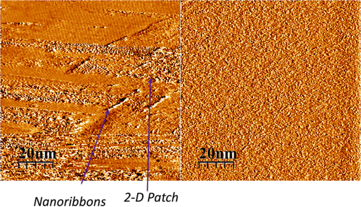
The detailed description of the methods used to synthesize epitaxial and functionalized graphene samples for this study can be found in earlier publications by the same authors13. The methods are summarized in the section below. The STM current in the presence of an external magnetic field was used to image both pristine EG and the same material after functionalization with the nitrophenyl radical precursor (NP-EG). Theory predicts that room-temperature magnetic order could be initiated along the edges and within relatively small 1-D and 2-D regions of functionalized graphene3,16. By changing the surface coverage area, it was possible to controllably synthesize a variety of finite size nanosegments of functionalized graphene. Figure 1a shows an STM image that contains functionalized regions of different shapes such as 1-D nanoribbons with a width of 3-nm and 2-D segments with characteristic sizes of approximately 20 nm. In this case, only about 5 to 10 percent of the total sample surface was covered with functionalized regions. Figure 1b shows a typical STM image of the pristine graphene surface, and for comparison purposes the STM images were taken at the same contrast level. The relatively strong image contrast in the functionalized case indicates a dramatic variation of the STM signal from adjacent sites particularly in the vicinity of the edges of the nanostructures. On the contrary, it can be noted that the image of the pristine surface is quite uniform and there is no visible difference in electron conduction (proportion to the local density of states (LDOS)) at different carbon sites.
Figure 1. STM images of functionalized and pristine graphene samples.
Typical equivalent STM images (of the feedback tunneling current necessary to maintain a constant separation between the probe and the surface) of (left) functionalized and pristine graphene samples.
A magnified STM image from functionalized carbon sites is shown in Figure 2a and the relationship of the functionalized sites to the bipartite graphene honeycomb structure is shown in Figure 2b. It can be seen that the sites with detectable STM signals are located only in a single sub-lattice (denoted here as B); the high-symmetry zigzag and armchair orientations are highlighted by red and green lines, respectively. A periodic signal can be observed along the high-symmetry orientations with two periods, 0.246 and 0.426 nm, along zigzag and armchair orientations, respectively, as clearly seen in both the experimental data and the auxiliary illustration. The maxima and minima in the super-lattice originate at the carbon sites in the B sub-lattice of the bi-partite graphene lattice, suggesting that preferential functionalization occurred in the A sub-lattice in this region of the sample15.
Figure 2. Bipartite Graphene Honeycomb.
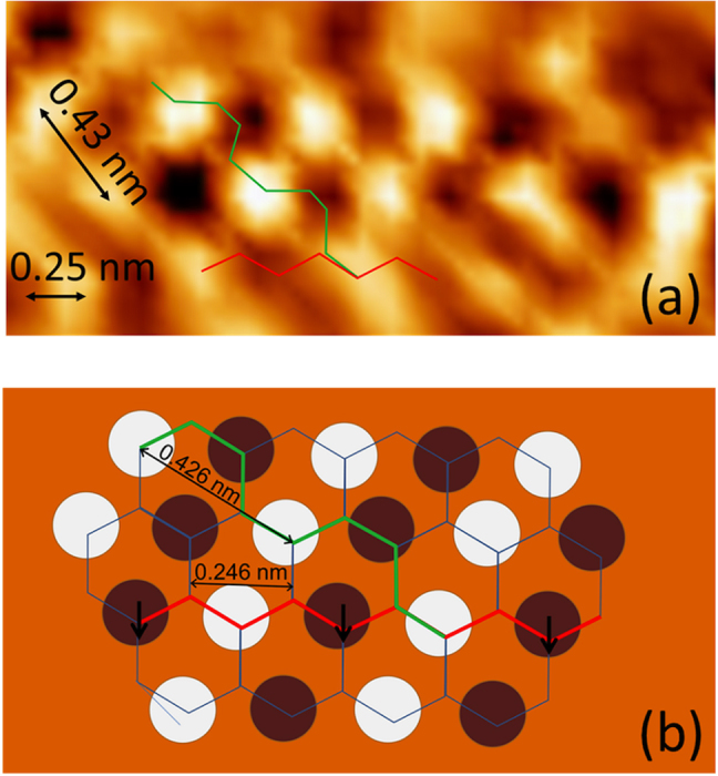
(a) A STM image of a periodic pattern. (b) An illustration of a potential anti-parallel spin configuration on the graphene surface (to relate to the STM image). The high-symmetry zigzag and armchair orientations are highlighted by red and green lines, respectively.
To study the magnetic field dependence of the STM super-lattice, we applied an approximately uniform out-of-plane magnetic field, which was kept constant along the X-scan lines but increased by a fixed step of 10 Oe after each 10 nm shift in the vertical (Y) direction as shown in Figure 3. It can be seen that the STM image contrasts from the functionalized nanoribbons along the zigzag orientation were reversed when the field was reversed; the highest local tunneling current (bright color) turned into the lowest current (dark color) and vice versa. The measurement indicates a relatively strong field dependence of the STM signal in the case of the functionalized nanoribbons. On the contrary, no change from the image shown in Figure 1b was observed in an external field for the pristine sample, as shown in supplementary information Figure S1.
Figure 3. Field Dependence of STM Imaging of Functionalized Graphene.
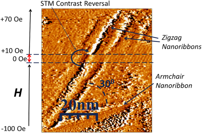
A field-dependent STM image of a functionalized region containing two zigzag nanibbons, one armchair nanoribbon, and 2-D segments. The field was varied in Y-direction from -100 to +70 Oe with a 10-Oe step.
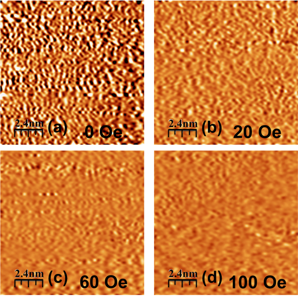
The field dependence of the STM image was further studied for the case of the 2-D functionalized finite-size segments. Four STM images of the same functionalized region taken at four out-of-plane field values, 0, 20, 60, and 100 Oe, respectively, are shown in Figures 4a-d. The clearly visible lines of periodic signals (indicative of a super-lattice with two signal levels), along high-symmetry orientations at zero field almost disappeared as the field was increased above 60 Oe.
Figure 4. Out-of-plane field effects.
Equivalent STM images of the same functionalized region at four different out-of-plane field values, (a) 0 Oe, (b) 20 Oe, (c) 60 Oe, and (d) 100 Oe.
To study the dependence on the field orientation, a similar experiment was conducted in the presence of an in-plane magnetic field. Three STM images of the same functionalized region were taken at three values of the in-plane field, 0, 5, and again 0 Oe, respectively, as shown in Figures 5a–c. It can be noted that even the low-strength field of 5 Oe was sufficient to fully eliminate the periodic patterns observed at zero field. After bringing the in-plane field back to zero, the super-lattice reemerged. The experiment indicates a relatively weak coupling of the super-lattice to the graphene structure.
Figure 5. In-plane field effects.
Equivalent STM images of the “same” area at different in-plane field values, (left) zero, (middle) 5 Oe, and (right) again zero.
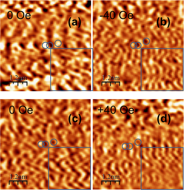
To investigate the field polarization effect on individual functionalized sites in more detail, the super-lattice was exposed to an out-of-plane field in both positive and negative directions, as shown in Figures 6a-d. The field was reduced from zero to −40 Oe and then gradually increased to +40 Oe. The field-dependent change of the STM signal (proportional to the LDOS) can be traced from the dynamics of the three circled sites in the above images. An important observation, which will be further discussed in the section below, is the hysteretic collective behavior of the sites in the pattern. The negative field of −40 Oe was sufficient to switch at least one of the two low conduction sites (seen as the two bright spots) into the high-conduction mode (changing the color from bright to dark). However, the positive field of +40 Oe was not sufficient to fully reverse the scenario, despite the obvious attempt to do so (as seen from the relative discoloration of the dark spots). This hysteretic behavior can be explained by the exchange coupling between adjacent functionalized sites, as described below in more detail.
Figure 6. Field Effects at Individual Functionalized Carbon Sites.
Equivalent STM images of the same region at four consequitive out-of-plane field values, (a) 0 Oe, (b) −40 Oe, (c) 0 Oe, and (d) +40 Oe. Three fixed sites of the functionalized graphene are highlighted in all the four images.
To understand how the field-influenced super-lattice depends on the different sample types under study, point contact I-V curves in an external out-of-plane field were measured from the pristine sample and the two regions of interest (nanoribbons and 2-D nano-segments) of the functionalized samples, as shown in Figures 7a–c, respectively. Clearly, no field dependence can be observed in the pristine sample (Figure 7a). On the contrary, a significant field-dependent gap widening can be detected in the functionalized samples and there is a substantial difference in the field dependence between the two functionalized regions. In Figure 7b, as the field was increased from −100 to +100 Oe, the I-V curve in the nanoribbon gradually changed from almost metallic (with no significant gap) to semiconductor-like (with a gap of over 1 V) after the field was reversed. On the other hand, the field dependence in the case of the functionalized 2-D segment shown in Figure 7c was highly non-linear (indicative of a complex collective behavior of the observed super-lattice) and the effect was obviously field polarized. Surprisingly, one can note that the conductance has drastically changed from metallic to insulator-like (with a gap of ~2 V) as the field was changed from −100 to −40 Oe.
Figure 7. Field dependence of I-V curves of point contacts for pristine and functionalized graphene.
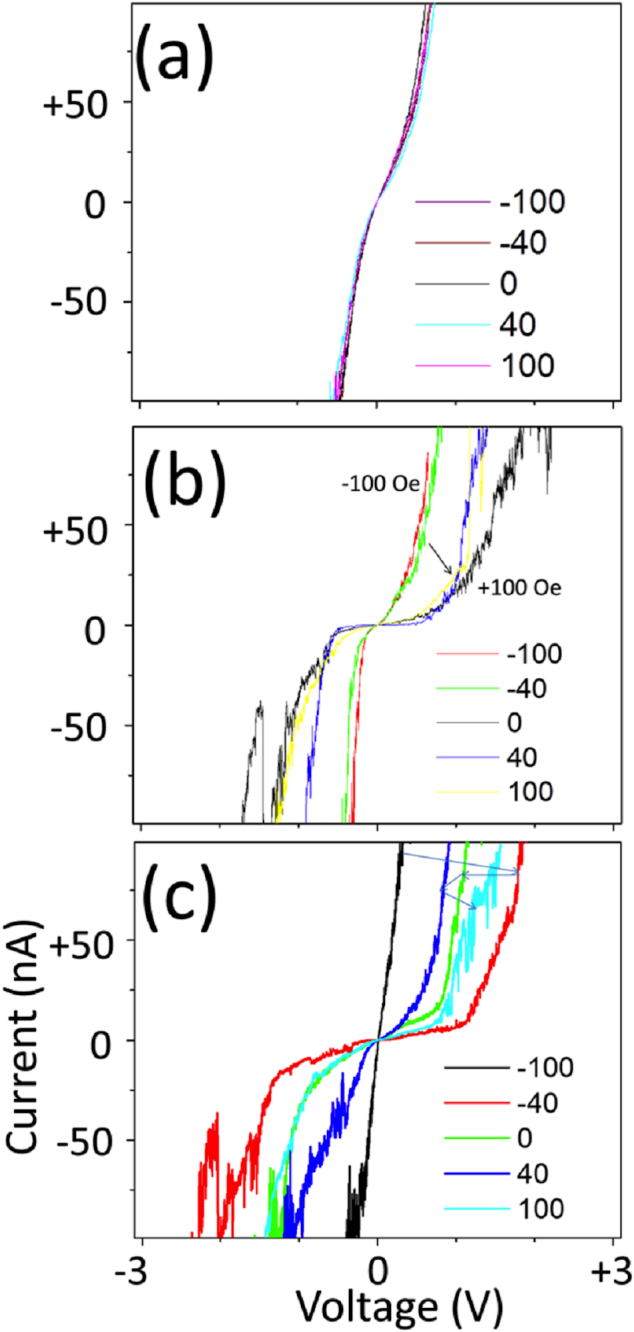
Point contact I-V curve (by a metallic PtIr probe) in the presence of an out-of-plane external magnetic field for (a) a pristine graphene, (b) a zigzag nanoribbon in a functionalized graphene, and (c) a 2-D 20-nm segment in a functionalized graphene. The blue arrows follow the field sequence to help understand the process of switching.
Discussion
The above measurements illustrated strong magnetic field dependence of the STM signal from the functionalized graphene. The important question to answer is whether the STM dependence could be related to the predicted presence of a magnetic order in the new material. Indeed, volume-averaged vibrating sample magnetometry (VSM) measurements indicated that the functionalized graphene could display a magnetic order at room temperature. (Typical in-plane and out-of-plane M-H hysteresis loops at room temperature are illustrated in supplementary information Figures S2 and S3. The M-H loops displayed (i) an insignificant out-of-plane anisotropy (~10 Oe), (ii) a presence of both ferromagnetic and antiferromagnetic coupling with an exchange field of 100 Oe. Finally, the average moment per functionalized carbon site was estimated to be of the order of 0.5 µB.) However, the volume-averaged VSM measurements cannot provide adequately detailed spin information with the atomic resolution which could be provided by scanning probe microscopy (SPM). Below we present the reason why we chose STM over the magnetic SPM techniques such as the popular magnetic force microscopy (MFM) and the high-resolution spin-polarized STM (SP-STM) 17.
To be able to distinguish magnetic information from individual carbon sites, it is hard to see how magnetic force microscopy (MFM) probes could provide the required spatial resolution of better than 0.15 nm (the separation between carbon atoms in graphene). The resolution of MFM probes is usually above 10 nm18. Furthermore, even low-moment magnetically coated probes can generate a local field of the order of 100 Oe that would override any periodic magnetic super-lattice with characteristic exchange and anisotropy fields of less than the field by the probe. Typical atomic force microscopy (AFM) and MFM images of pristine and functionalized patches of the epitaxial graphene samples are shown in supplementary information Figure S4. The graphene in these patches act as a soft magnetic material relative to the field generated by the CoCr-based MFM probe (of the order of 0.5 kOe). As a result, though the image indeed indicates the presence of magnetic order in functionalized graphene, the information provided by this technique is limited because of the low spatial resolution and the destructive effect of the stray magnetic field generated by the probe. As for the SP-STM approach, indeed it is the only SPM mode that allows resolving spin information with an angstrom resolution. However, the potential question of overriding the spin information with the stray field generated by the probe itself (of the order of 100 Oe) remains open because the field is comparable to the value of the projected exchange field in the functionalized graphene at room temperature. Nevertheless, a further detailed SP-STM study might be necessary to further understand the phenomenon.
Going back to the analysis, the above STM measurements indicate that both the STM super-lattice images and the point contact I-V curves strongly depend on the external magnetic field for the functionalized samples while no dependence can be detected for the pristine sample. The STM signal is the feedback tunneling current change necessary to maintain a programmed separation of a few angstroms between the probe and the sample surface. The current change reflects the surface texture of the sample; however, it also depends on the local density of states that can be spin polarized. The observed super-lattice resembles the periodic spin pattern which was theoretically predicted in finite size 1-D and 2-D graphene regions3, assuming that the spin up and spin down electrons conduct current differently (according to the half-metallicity theory). The only difference is the fact that the super-lattice includes functionalized graphene sites on one graphene, A or B, sub-lattice only. According to the original theoretical predictions, both graphene sublattices A and B are expected to participate in the magnetic order (with spins on each sublattice aligned ferromagnetically). As described above, in the current experiment functionalizations are covalently bonded to one sublattice only and consequently lead to the accumulation of spins in the other sub-lattice. However, our measurements indicate that both parallel (ferromagnetic) and anti-parallel (antiferromagnetic) magnetic orders might be present in the super-lattice. Another difference between the current functionalized and theoretical defect-induced ferromagnetic graphene systems is the nature of the host of the super-lattice. The predicted ferromagnetism is due to itinerant electrons while the observed magnetic order takes place in a semiconducting host (triggered by the above functionalization). A possible theoretical foundation for the magnetic order in the semiconducting graphene host was also proposed19. A further theoretical study might be necessary to understand the ground states of the system depending on the dimensions and geometry of nanostructures.
An important open question relates to the physics that underlies the magnetic field dependence of the STM contrast. Although a detailed theoretical study still needs to be developed, we consider a number of possibilities to explain the experimental data. First, we assume that we can neglect the contribution of spin polarized effects due to the interaction (through polarized currents) of the spins in the graphene with the spins in the marginally paramagnetic Pt-Ir probe. Under the relatively small external field (of 100 Oe), only a negligible fraction of the electrons in the probe is expected to be polarized. An obvious test would be to use the probe to image relatively well-understood magnetic systems, e.g., a CoCr-based perpendicular magnetic recording medium, in which ultra-high-density magnetic information is pre-recorded using a commercial data storage spinstand18. Indeed, STM imaging of different magnetic and non-magnetic surfaces with the same Pt-Ir probe displayed no contrast, as shown in supplementary information Figure S4. Therefore, we can conclude that the observed field dependence is inherent to the functionalized graphene surface itself. Second, despite the promising property of half-metallicity, in the current setup it is hard to argue that the local conductance can be spin-polarized by the local electric field due to the current between the STM probe and the graphene surface. Using the above nanoribbon (Figure 3) as a case study, the local electric field (across a nanoribbon) by the STM probe must reverse its direction when the probe is moved across the two edges (of the nanoribbon). However, if we assume that the spins at the opposite edges are coupled antiferromagnetically and the nanoribbon is half-metalic, the local conductance must not be spin polarized. At least one spin direction must be conducting in either case and consequently no STM contrast is expected. Third, the contrast reversal (with the field reversal) in the STM image of the 3-nm zigzag nanoribbons in the functionalized graphene (Figure 3) cannot be explained just by the reversal of the spins. Here, we assume the ground state with parallel (ferromagnetic) coupling along the edges and anti-parallel (anti-ferromagnetic) coupling across the edges20. By symmetry of the system, an out-of-plane magnetic field cannot reverse both spins in an anti-ferromagnetic system (assuming an out-of-plane anisotropy), though it can align both spins in the same direction by overcoming the exchange coupling (Figure S3b). Ideally, an external field can break the symmetry between the two spin orientations and bring the energy band of one of the orientations to the Fermi level and thereby produce spin-polarized conductance. However, the field required to move the energy level of a particle with a 0.5 µB moment by 1 eV would be many orders of magnitude higher than the relatively negligible applied field (of 100 Oe) in the current experiment. Therefore, we hypothesize that the external field triggers some effective out-of-plane biasing intrinsic field (exchange field) that breaks the time reversal symmetry. For example, the effective field can be due to the exchange coupling of the functionalized layer to the graphene layer(s) underneath (if the layer can be spin polarized) or to oxide based magnetic impurities which are hard to completely eliminate in this system. Consequently, by directing the moment of the exchange-biasing component, the external field controls the spin-polarized conductance.
Such spin-polarized conductance, indicative of half-metallic behavior, is in agreement with the dramatic change of the effective gap in the point contact I-V curve ( Figure 7b), from a negligibly low value to over 1 V as the field is changed from negative to positive. Another observation related to the nano-segment is the fact that a relatively small field (of less than 10 Oe) is sufficient to rotate spins from an out-of-plane to in-plane direction while the anti-parallel coupling between the spins cannot be broken until the field is increased above 100 Oe (Figures 5a–c). The reemergence of the super-lattice after the field is brought back to zero indicates the out-of-plane anisotropy of the observed spin pattern. This observation implies that the anisotropy field that couples the spin super-lattice to the graphene structure is less than 10 Oe, while the exchange field that maintains the coupling between the adjacent spins is of the order of 100 Oe (the maximum applied out-of-plane field).
It can be noted that in the case of 2-D segments the functionalized carbon sites also display an STM super-lattice, now mostly in the form of connected 1-D periodic sub-regions along the main graphene symmetry orientations (zigzag and armchair). Because the magnetic anisotropy, though relatively small, is in the out-of-plane orientation, such a super-lattice and its field dependence can be especially well observed in the experiment with an external out-of-plane magnetic field (Figures 4a–d). As shown in Figure 4a, the super-lattice at zero field, shows a polycrystalline arrangement. With diminished edge effects, the ground state has mostly anti-parallel spin coupling within the sub-regions of the 2-D segment. The fact that the super-lattice contrast almost disappeared at an out-of-plane field of above 60 Oe (Figures 4b–d) might be indicative of the exchange field being above 60 Oe for the anti-parallel spin coupling. The experiment described in Figures 6a–d illustrates the process of spin reversal at individual functionalized sites. Unlike a nanoribbon, a nanosegment, because of its finite sizes (and therefore the finite number of involved graphene sites) can be in the ground energy state that can include a spin configuration with a non-zero net magnetic moment. To be able to track the spin dynamics of individual carbon atoms, three spin-bearing sites (circled) were selected with unique positions with respects to each other and the rest of the array. At the initial zero field, two of the spins are directed up (bright color) and the remaining spin is directed down (dark color). It can be seen that a field of −40 Oe is sufficient to reverse only one of the two up spins (Figure 6b). As expected, no significant change is observed as the external field is brought back to zero (Figure 6c). Now, the oppositely directed field of +40 Oe is not sufficient to reverse the two down spins. The experiment indicates that the exchange coupling between the spins is higher than 40 Oe in this field orientation. The point contact I-V curve for this sample (Figure 7c) follows the field dependence that is correlated with the switching of an individual functionalized carbon site. At this particular point contact, the field of −100 Oe seems to enable a high value of LDOS (with absolutely no visible gap). As the field is increased to −40 Oe, the LDOS value quickly reaches the low end of the spectrum (the maximum gap). This is consistent with the model according to which the exchange coupling can be broken at a field magnitude of 100 Oe and therefore the spin must be in the “up” direction at this field value. (The first experiment indicated the exchange field of the order of 60 Oe to break the exchange coupling.) Then, as the field is increased to −40 Oe, the super-lattice reemerges with the spin-bearing site in the vicinity of the contact having its spin down (open gap case). Though the spin experiences some variation as the field is further increased to +100 Oe, the site still remains in the open-gap mode.
In conclusion, correlated field studies of STM images and point contact I-V curves in functionalized and pristine epitaxially-grown graphene indicate parallel (ferromagnetic) and anti-parallel (antiferromagnetic) magnetic order in functionalized 1-D zigzag nanoribbons and anti-parallel spin order in 2-D nano-segments with characteristic sizes of over 20 nm at room temperature; the average surface coverage by the magnetically ordered functionalized carbon sites is less than 10 percent. The field-dependent experiments suggest an anisotropy field of less than 10 Oe and an exchange field of 100 Oe in the functionalized samples. No comparable field dependent effects and magnetic super-lattices can be detected in the pristine epitaxial graphene samples.
Methods
This section summarizes the methods previously developed by the authors to fabricate the epitaxial and functionalized graphene samples for this study10,12. The samples consist of 5–10 layers of epitaxial graphene with a structural coherence of 300 nm; the EG samples were grown in vacuum on the [0001] face of diced SiC wafers (dimension 3.5 mm × 4.5 mm) after surface flattening by hydrogen etching2. The graphene substrates were chemically functionalized with nitrophenyl groups by spontaneous electron transfer to the corresponding diazonium salt as described previously; this solution-based, room temperature chemical functionalization procedure is exceedingly gentle and leads to the covalent attachment of the aryl groups to the basal plane carbon atoms in the top graphene layer10.
Author Contributions
Jeongmin Hong performed key measurements including AFM, MFM, and STM studies. Elena Bekyarova and Robert Haddon functionalized epitaxial graphene. Ping Liang helped establish experimental procedures. Walt de Heer fabricated epitaxial graphene samples. Sakhrat Khizroev designed and oversaw the project.
Supplementary Material
Room-temperature magnetic ordering in functionalized graphene
Acknowledgments
We acknowledge financial support from DOD/DMEA under contract H94003-09-2-0904, NSF-MRSEC through contract DMR-0820382, and NSF award 005084-002.
References
- Geim A. K. & Novoselov K. S. The rise of graphene. Nat. Mater. 6, 183–191 (2007). [DOI] [PubMed] [Google Scholar]
- de Heer W. A. et al. Epitaxial graphene electronic structure and transport. J. Phys. D: Appl. Phys. 43, 374007 (2010). [Google Scholar]
- Yazyev O. V. Emergence of magnetism in graphene materials and nanostructures. Rep. Prog. Phys. 2010, 73, 056501 (2010). [Google Scholar]
- Son Y.-W., Cohen M. L. & Louie S. G. Half-metallic graphene nanoribbons. Nature 444, 347–349 (2008). [DOI] [PubMed] [Google Scholar]
- Yazyev O. V. & Helm L. Defect-induced magnetism in graphene. Phys. Rev. B 75, 125408 (2007). [Google Scholar]
- Yazyev O. V. Magnetism in disordered graphene and irradiated graphite. Phys. Rev. Lett. 101, 037203 (2008). [DOI] [PubMed] [Google Scholar]
- Nair R. R. et al. Spin-Half paramagnetism in graphene induced by point defects. Nature Phys. 8, 199–202 (2012). [Google Scholar]
- Pisani L., Montanari B. & Harrison N. M. A Defective Graphene phase predicted to be a room temperature ferromagnetic semiconductor. New J. Phys. 10, 033002 (2008). [Google Scholar]
- Hong J. et al. Effect of nitrophenyl functionalization on the magnetic properties of epitaxial graphene. Small 7, 1175–1180 (2011). [DOI] [PubMed] [Google Scholar]
- de Groot R. A., Mueller F. M., van Engen P. G. & Buschow K. H. New class of materials: half-metallic ferromagnets. Phys. Rev. Lett. 50, 2024–2027 (1983). [Google Scholar]
- Kobayashi Y., Fukui K., Enoki T., Kusakabe K. & Kaburagi Y. Observation of zigzag and armchair edges of graphite using scanning tunneling microscopy and spectroscopy. Phys. Rev. B 71, 193406 (2005). [Google Scholar]
- Bekyarova E. et al. Chemical modification of epitaxial graphene: spontaneous grafting of aryl groups. J. Am. Chem. Soc. 131, 1336–1337 (2009). [DOI] [PubMed] [Google Scholar]
- Bekyarova E., Sarkar S., Niyogi S., Itkis M. E. & Haddon R. C. Advances in the chemical modification of epitaxial graphene. J. Phys. D: Appl. Phys. 45, 154009–18 (2012). [Google Scholar]
- Zhang H. et al. Aryl functionalization as a route to band gap engineering in single layer graphene devices. Nano Lett. 11, 4047–4051 (2011). [DOI] [PubMed] [Google Scholar]
- Niyogi S. et al. Covalent chemistry for graphene electronics. J. Phys. Chem. Lett. 2, 2487–2498 (2011). [Google Scholar]
- Lieb E. H. "Two theorems on the Hubbard model." Phys. Rev. Let. 62, 1201–1204 (1989). [DOI] [PubMed] [Google Scholar]
- Wiesendanger R. Spin mapping at the nanoscale and atomic scale. Rev. Mod. Phys. 81, 1495–1550 (2009). [Google Scholar]
- Amos N., Ikkawi R., Haddon R., Litvinov D. & Khizroev S. Controlling multi-domain states to enable sub-10-nm magnetic force microscopy. Appl. Phys. Lett. 93, 203116 (2008). [Google Scholar]
- Pisani L., Montanari B. & Harrison N. M. A defective graphene phase predicted to be a room temperature ferromagnetic semiconductor. New Journal of Physics 10, 033002 (2008). [Google Scholar]
- Fujita M., Wakabayashi K., Nakada K. & Kusakabe K. Peculiar localized state at zigzag graphite edge. J. Phys. Soc. Jpn. 65, 1920–1923 (1996). [Google Scholar]
Associated Data
This section collects any data citations, data availability statements, or supplementary materials included in this article.
Supplementary Materials
Room-temperature magnetic ordering in functionalized graphene


