Abstract
Morphological and optical characteristics of radio frequency-sputtered zinc aluminum oxide over porous silicon (PS) substrates were studied before and after irradiating composite films with 130 MeV of nickel ions at different fluences varying from 1 × 10¹² to 3 × 10¹³ ions/cm2. The effect of irradiation on the composite structure was investigated by scanning electron microscopy, X-ray diffraction (XRD), photoluminescence (PL), and cathodoluminescence spectroscopy. Current–voltage characteristics of ZnO-PS heterojunctions were also measured. As compared to the granular crystallites of zinc oxide layer, Al-doped zinc oxide (ZnO) layer showed a flaky structure. The PL spectrum of the pristine composite structure consists of the emission from the ZnO layer as well as the near-infrared emission from the PS substrate. Due to an increase in the number of deep-level defects, possibly oxygen vacancies after swift ion irradiation, PS-Al-doped ZnO nanocomposites formed with high-porosity PS are shown to demonstrate a broadening in the PL emission band, leading to the white light emission. The broadening effect is found to increase with an increase in the ion fluence and porosity. XRD study revealed the relative resistance of the film against the irradiation, i.e., the irradiation of the structure failed to completely amorphize the structure, suggesting its possible application in optoelectronics and sensing applications under harsh radiation conditions.
Keywords: Porous silicon, Zinc aluminum oxide, Swift heavy ions, Photoluminescence, Cathodoluminescence.
Background
Nowadays, efforts are being made to look for suitable types of nanocomposites for optoelectronic applications. Semiconductor nanocrystallites have been considered as the emission source for the next-generation light-emitting diodes due to their electro-optical properties and tunable size [1,2]. Zinc oxide (ZnO) with trivalent elements such as aluminum (Al) is a unique n-type semiconductor and transparent material with a direct bandgap of 3.37 eV, along with a large exciton binding energy of 60 meV [3]. Al-doped ZnO (AZO) is considered as an important material for its application as a transparent electrode in flat panel displays [4] due to its high conductivity and good transparency. Till now, AZO films with resistivity lower than 1 to 5 × 10⁻⁴ Ω cm [5-7] and transmittance more than 85 % have been attained. On the other hand, porous silicon (PS) has been investigated due to its room-temperature luminescence, and efforts have been focused to obtain an efficient electroluminescent (EL) device [8] based on PS for its possible integration with the present microelectronic industry. Along with various semiconducting and piezoelectric properties suitable for various applications in the optoelectronic industry, the EL efficiency could be increased strongly by filling the pores of PS with AZO. Due to the open structure and large surface area, together with the unique optical properties, PS is a good candidate for a template. It is known that the emission energy of PS increases with a decrease in silicon nanocrystallite size covering the entire visible spectrum from red to blue [9]. It has been reported that the blue luminescence band with a relatively fast decay time is observed in the oxidized PS samples. On the other hand, it is easy to get the red emission from the PS, and if it could be added with any other semiconductor with emission in the blue green region, it could be useful to obtain the white light through a simple route for possible applications like the display technology [4,10]. Apart from that, our group recently demonstrated the importance of PS-ZnO composites for sensing application through a control over the spacial distribution of zinc oxide and its transport properties on the porosity of the PS substrate [11].
In the last few years, a considerable amount of progress has been done to enhance the optical properties and other physical characteristics of the ZnO film with different techniques. Among them, energetic ion beams have been employed to modify the electrical, optical, and structural properties of different materials [12-15]. Matsunami et al. [16] studied the effect of irradiation on the electrical, structural, and optical properties of indium-doped ZnO films and found an enhancement in the electrical conductivity. Sugai et al. [17] reported a two-order increase in the conductivity of AZO films after irradiation with Ni and Xe ions. Recently, Singh et al. [18] have reported an increase in the ethanol sensing response of irradiated SnO2 films with ZnO demonstrating a strong resistance to damage caused by ion irradiation. Another work on ZnO-PS nanocomposites [19], where ZnO deposited onto the microporous silicon with sol–gel technique, showed the suppression of X-ray diffraction (XRD) peaks after irradiating it with heavy ions (Au). Hence, the effect of high-energy light ions (such as nickel) could be interesting in studying the stability of the ZnO structure along with its optical properties. In this work, we have investigated the ion irradiation effects on AZO films deposited onto the mesoporous silicon substrate and shown a white light emission from the resulting composites after irradiating with high-energy nickel ions. Swift heavy ion (SHI)-induced morphological and structural changes, in terms of XRD and scanning electron microscopy, have also been studied. The emission after 325-nm excitation from a xenon arc lamp has been compared with the cathodoluminescence (CL) in studying the modifications in the deep-level defects induced by the high-energy radiations. Comparison between the low- and high-porosity mesoporous substrates is also presented. The nanocomposites are found to retain the crystalline structure after irradiation.
Methods
PS samples were fabricated by wet electrochemical etching of p++-type Si(100) wafers with a resistivity of 0.01 to 0.05 Ω cm and at different current densities of 10 (LP) and 70 mA/cm2 (HP) using a 3:7:1 solution of HF/ethanol/glycerol. The porosity of samples LP (low porosity) and HP (high porosity) was 50 % and 70 %, respectively. The thickness of both samples was kept to 7 μm. After the fabrication, the samples were rinsed with ethanol and dried in pentane.
In order to study the effect of PS on PL and other structural and transport properties, AZO films were deposited by radio frequency magnetron sputtering. A sputtered target with a mixture (2 wt.% Al2O3-ZnO) was used, and the PS substrate temperature was kept at 300 °C during the deposition of the AZO film with a thickness of 150 nm. After deposition, the low- and high-porosity PS-AZO composites were named as ZLP and ZHP, respectively. As-deposited films were later annealed at 700 °C for 1 h in the tubular furnace in argon atmosphere. The annealed films were irradiated with 130-MeV nickel ions using the 15UD Pelletron Accelerator at the Inter University Accelerator Centre, New Delhi. The samples were mounted on a rectangular-shaped ladder and were irradiated in high vacuum chamber. The focused ion beam was scanned over an area of 1 × 1 cm2. The films of low porosity (ZLP) were irradiated with fluences of 1 × 10¹² and 3 × 10¹³ ions/cm2, and the films of high porosity (ZHP) were irradiated with fluences of 3 × 10¹² and 1 × 10¹³ ions/cm2. The beam current was kept constant at approximately 1.5 pnA. The electronic stopping power (energy dissipated in electronic excitations) and nuclear stopping power (energy dissipated in atomic collisions) by such ions in ZnO are around 24.63 and 0.44 keV/nm, respectively (calculated using SRIM2003 simulation code). The modifications in the properties of ZnO films are expected to be mainly due to the electronic excitations, though the contributions of small nuclear stopping power could not be ignored.
The structural properties and the thickness of the PS and nanocomposites were analyzed using a high-resolution field emission scanning electron microscope (SEM; JSM-7401 F, JEOL Ltd., Akishima-shi, Japan). The orientation and crystallinity of the ZnO crystallites were analyzed using an X-ray diffractometer (X'Pert PRO, PANalytical B.V., Almelo, The Netherlands) using CuKα radiation having a wavelength of 1.54 Å. PL properties were studied using a Varian Fluorescence spectrophotometer (Cary Eclipse, Agilent Technologies, Inc., Santa Clara, CA, USA) under the excitation by 325-nm photons using a 500-W xenon lamp. CL spectroscopy was done using JEOL JSM 5300 SEM with an electron beam energy of 15 keV. CL measurements were performed at 100 K in the UV-visible spectral range using a Hamamatsu R928P photomultiplier (Hamamatsu, Japan). A SPEX 340-E computer-controlled monochromator (Metuchen, NJ, USA) was used for the spectral analysis.
Results and discussion
X-ray diffraction
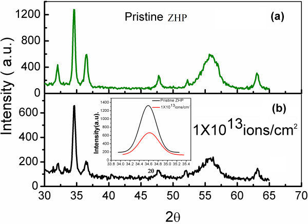
The crystalline nature of the PS-AZO film was studied through XRD spectra (Figure 1) of pristine and irradiated samples at different fluences. The pristine PS-AZO film had a polycrystalline hexagonal wurtzite structure as confirmed by the dominant (002) peak. The ZHP sample, after irradiation at a fluence of 1 × 10¹³ ions/cm2, demonstrates a relative decrease (of about 50 %) in the peak intensities corresponding to the zinc oxide (i.e., (100), (002), and (101) peaks) and PS (at 2θ = 55°), indicating a decrease in the degree of crystallinity of the composite, after irradiation. Apart from this, a slight shift of 2θ = 0.02° in the (002) peak is observed after applying Gaussian fit and is attributed to the release of strain in the crystallites, similar to the effect reported earlier by Rehman et al. [18] (shown as inset in Figure 1b). Applying Scherrer's formula for the (002) peak, the crystallite size is found to decrease from 23.74 to 20.46 nm. The decrease in the crystallite size at a fluence of 1 × 10¹³ ions/cm2 could be attributed to the sputtering induced by the SHI irradiation, which is in accordance with the effect observed by some other groups [12,20,21]. The changes in the peak intensities for the samples with the low-porosity PS (10 mA/cm2) substrate show similar but less intense effects after irradiation at a fluence of 3 × 10¹³ ions/cm2. A relative dependence of the crystalline quality can be attributed to the substrate porosity dependence of ZnO grain growth [11] and its physical stability. The presence of the low-porosity silicon substrate tends to contribute in the retention of the physical and optical characteristics (shown in the later part of the manuscript). The above-mentioned result can be inferred as an opening for the possible optoelectronic application of PS-AZO films under harsh radiation conditions.
Figure 1.
XRD spectra of PS-AZO nanocomposite corresponding to ZHP (PS substrate fabricated at 70 mA/cm2). (a) Pristine and (b) after irradiation at a fluence of 1 × 10¹³ ions/cm2. The inset shows the comparison of the (002) peak before and after irradiation.
Measurement of bandgap by optical method
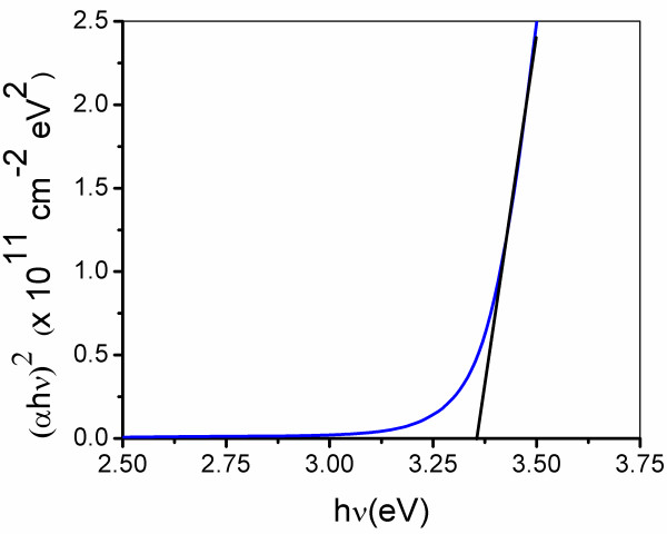
For determining the bandgap of the ZnO film, the absorption coefficient (α) is obtained from transmittance data using the following equation:
where d is the thickness of the film and T is the optical transmittance.
The bandgap can be estimated using the equation
| (1) |
where h is the Planck constant, ν is the frequency of the incident photon, and A is a constant. Hence, from Figure 2, the estimated optical bandgap of the film is 3.35 eV, involving direct electronic transitions [22,23].
Figure 2.
Bandgap calculation of AZO film from UV–vis spectroscopy. (αhν)2 vs. hν (photon energy) plot of zinc oxide film deposited over the glass substrate.
Scanning electron microscopy
In order to check the morphological changes, secondary electron microscope images (Figure 3) were analyzed before (pristine) and after irradiation for the ZHP sample. Before irradiation, the films are found to have regular flaky grains spread uniformly over PS. The size of the grains before irradiation appears to be uniform and is in the range of 50 to 90 nm. However, the irradiated film (at a fluence of 1 × 10¹³ ions/cm2) shows apparent changes in the morphology which could be attributed to the inelastic collisions between the electrons of the target material and the high-energy ions. Most of the flaky structure appears as irradiation-induced dark patches (Figure 3b). The observed phenomenon after irradiation is similar to the one reported by Rehman et al. [20]. The observed changes in the morphology could be co-related to the results of XRD studies.
Figure 3.
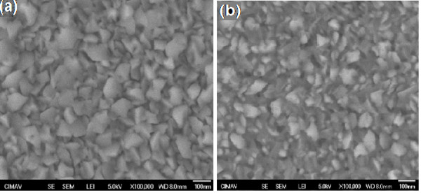
SEM images corresponding to ZHP (PS-AZO). (a) Pristine and (b) after irradiation at a fluence of 1 × 10¹³ ions/cm2.
Photoluminescence spectroscopy
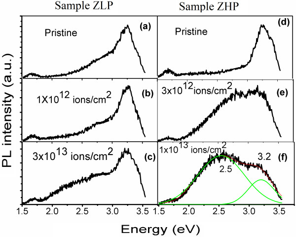
The photoluminescence (PL) characteristics of the PS-AZO nanocomposite were studied (Figure 4) before and after SHI irradiation using nickel ions with a low-energy beam of 130 MeV. Figure 4a shows the PL spectrum of the composite formed with the ZLP substrate, with a peak around 3.25 eV attributed to the band-edge excitonic transition of ZnO [24,25]. The PL emission peak shows a low-intensity shoulder/tapering end at the left-hand side of the peak which can be attributed to the well-known oxygen vacancies in the zinc oxide layer [26-28]. Although the origin of this broad defect emission is controversial, it has been attributed to the singly ionized oxygen vacancies (Vo−) [27] and interstitial oxygen (Oi) [27,28]. Particularly, a ZnO emission of 2.5 eV has been assigned to the recombination of delocalized electrons close to the conduction band with deeply trapped holes in Vo+ centers. Figure 4b shows PL emission from the PS-AZO nanocomposite with low-porosity substrate (i.e., made with a current density of 10 mA/cm2) after irradiation at a fluence of 1 × 10¹² ions/cm2. No significant change in the defect-related PL intensity around 2.5 eV was observed, proving the stability of the structure up to a certain degree of irradiation fluences. On the other hand, an increase in the degree of fluence to 3 × 10¹³ ions/cm2 generated a significant increase of the PL intensity corresponding to the defects centered at 2.5 eV in Figure 4c, which is attributed to an increase in the deep-level defects, possibly oxygen vacancies. The formation of defects can be further understood as follows: As the SHI penetrates the solid, inelastic collisions are expected between the ion and the target electrons. In general inelastic collision, it is believed that electronic excitation and ionization of the target atoms plays a dominant role for high-energy heavy ion impact on ZnO. In the case of SHIs, inelastic nuclear collision results in the energy transfer which can yield localized heating/amorphization and a significant increase in the number of defects. On the other hand, due to the fact that in this energy range, electronic stopping is much bigger than nuclear stopping, electronic excitation caused by strong electronic stopping can weaken oxygen bonds, resulting in the formation of oxygen vacancies [29].
Figure 4.
PL spectra of PS-AZO nanocomposites irradiated at different fluences. (a) Pristine, (b) irradiated with 1 × 10¹² ions/cm2, and (c) 3 × 10¹³ ions/cm2 correspond to the ZLP sample. (d) Pristine, (e) irradiated with 3 × 10¹² ions/cm2 and (f) 1 × 10¹³ ions/cm2 correspond to the ZHP sample.
Although a similar behavior was observed for the ZHP sample as well (see Figure 4e,f), an increase of fluence is shown to enhance significantly the defect-related emission centered at 2.5 eV. The peaks corresponding to 2.5 to 3.25 eV have been observed to merge, resulting in the formation of broad white emission band from 3.25 to 1.50 eV. In comparing Figure 4e,f, a further increase in the level of fluence is found to increase the signal corresponding to the defects (2.5 eV) with a simultaneous decrease in the band-edge emission (3.25 eV). The intensity of the emission band corresponding to PS (around 1.7 eV) is found to decrease slightly with an increase in the level of fluence which is in accordance to the already reported work of Singh et al. [19]. The resulting PL spectra are observed to have an almost white emission from the composite structure which can be very useful for the display devices.
Cathodoluminescence
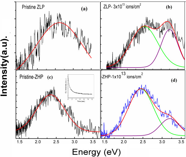
In order to further investigate the defect-related luminescence mechanisms, CL spectroscopy was performed on all the composite samples. The main advantage of the CL is the spacial resolution, determined by the distribution of the excess carrier in the material and is therefore not limited by the diffraction in the collection and excitation optics, which is very customary in all the far-field techniques. Hence, to enhance our understanding regarding the optical properties of PS-ZnO composites under irradiation conditions, the PL studies have been complimented by CL analysis. The major reason that very few studies reported CL of PS is due to an extremely weak and unstable data. The inset in Figure 5c shows a strong decrease of the CL emission signal of the PS produced by the electron beam irradiation in SEM. Deposition of AZO layer on the mesoporous silicon layer leads to the stability of the composite structure. As the electron beam can inject into the samples, a strong charge density produces saturation of radiative levels; hence, the luminescence from defects can be explored in detail. Figure 5a shows CL spectra from the non-irradiated (pristine) sample with a broad emission centered at about 2.6 eV, which apparently corresponds to the ZnO defect emission centered at 2.5 eV in PL spectra. The low-intensity CL recorded in the spectra is attributed to the low sensibility of our system at room temperature. As compared to the PL spectra from the pristine sample, the ZnO band edge emission was not resolved in CL spectra, possibly due to presence of a high density of defects in the film-substrate interface. Figure 5b shows the CL spectra from the irradiated ZLP sample, revealing two emissions centered at 3.2 and 2.5 eV, associated to the ZnO band edge and defect emission. As commented in the ‘Photoluminescence spectroscopy’ section, the 2.5 eV band is associated to the presence of oxygen vacancies and other native defects [30-32]. The CL spectrum of the ZHP sample shows a similar behavior as that of the ZLP sample (Figure 5c,d), with the generation of the ZnO band edge (3.2 eV) after the SHI irradiation. This effect is not correlated with PL measurements, where the relative intensity of UV emission decreased after irradiation (Figure 4c,f). In CL measurements, an increase of the relative intensity of the ZnO band edge emission typically corresponds to an improvement of the crystalline quality, mainly due to annealing effects [30,33]. Possibly, the SHI irradiation generated a high density of point defects mostly at the film's surface, which was recorded in PL spectra with a relative increase of the 2.5 eV emission (Figure 4c,f), while at the film-substrate interface, the irradiation-generated heating produces annealing of defects (enhancement of crystalline behavior) as shown in the corresponding CL spectra (Figure 5b,d).
Figure 5.
CL spectra of PS-AZO nanocomposites irradiated at different fluences. (a) Pristine ZLP sample. (b) ZLP sample irradiated with 3 × 10¹³ ions/cm2. (c) Pristine ZHP sample. (d) ZHP sample irradiated with 1 × 10¹³ ions/cm2.
Electrical properties
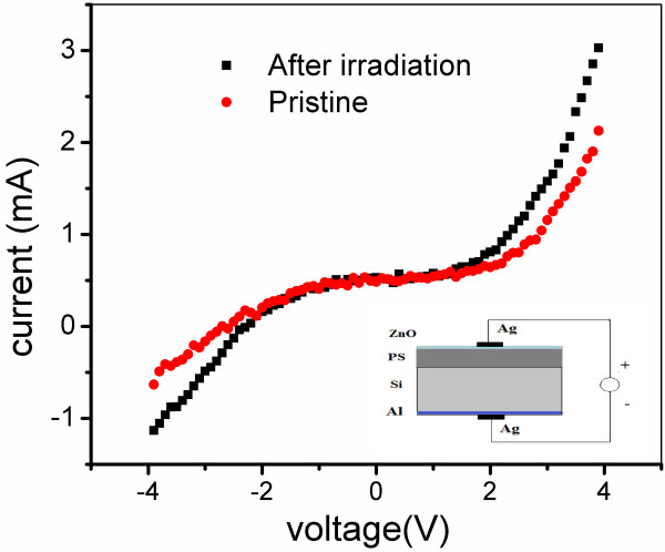
Figure 6 demonstrates the non-ohmic electrical response of the current–voltage (I-V) measurements performed in a two-terminal AZO-PS-Si configuration (inset of Figure 6) which is normally attributed to the formation of Schottky barriers at the ZnO-PS interfaces. It was seen that after irradiation at 1 × 10¹³ ions/cm2, the ZHP sample shows little higher forward/reverse current than the pristine sample. In order to quantify the deviation from the Schottky behavior, the rectifying factor (IF/IR) was calculated at 4 V and was found to be 3.34 and 2.62 for the pristine ZHP sample and that after irradiation (1 × 10¹³ ions/cm2 of fluence), respectively. A slight reduction in the rectifying factor after irradiation can be attributed to the irradiation-induced thermal annealing of the defects and hence an improvement of the crystallinity at the interface of ZnO-PS.
Figure 6.
I-V curves of ZnO-PS structure (ZHP sample) in a sandwich configuration, measured at room temperature. The voltage varies from −4 to 4 V with a sweep rate of 150 mV/s. The inset in the lower part shows the schematic of the configuration used for I-V characteristics. The inset of Figure 5c shows CL emission spectra as a function of time showing the degradation of the as-etched PS layer by high-energy electrons.
Conclusions
We report the substrate porosity and fluence-dependent white light emission from RF-sputtered zinc aluminum oxide deposited on PS after SHI irradiation. The structures are shown to partially retain their crystallinity, when irradiated with light Ni ions. Composites are found to have a rectifying behavior which reduces by a factor of 0.78 after irradiation. Its stability under harsh irradiation conditions makes it useful for space applications. Apart from that, the tunability in the optical properties is important for optoelectronic applications.
Competing interests
The authors declare that they have no competing interests.
Authors' contributions
YK made the porous silicon samples and performed their characterization before and after irradiation. MHZ participated in performing the cathodoluminescence studies and their corresponding analysis. SFOM participated in acquiring the SEM and XRD facilities. FS performed the SHI irradiation at IUAC, New Delhi. XM participated in the deposition of AZO film on PS and glass substrates. VA conceived the study, participated in its design and coordination, and codrafted the manuscript with YK. All authors read and approved the final manuscript.
Authors' information
YK is a Ph.D. student registered at CIMAV, Chihuahua, and is doing his research work at CIICAp, UAEM, Mexico. MHZ is an associate professor at CNyN, UNAM and is working on the characterization of semiconductor nanostructures. SFOM is working as a researcher at CIMAV, Chihuahua, in the field of nanostructured materials. FS is a scientist at IUAC, New Delhi. XM is a senior scientist at CIE, UNAM working on thin film semiconductors for photovoltaic applications.VA is working as a professor investigator at CIICAp, UAEM in the field of nanostructured silicon.
Contributor Information
Yogesh Kumar, Email: vivsaluja@yahoo.com.
Manuel Herrera-Zaldivar, Email: zaldivar@cnyn.unam.mx.
Sion Federico Olive-Méndez, Email: sion.olive@cimav.edu.mx.
Fouran Singh, Email: fouran@gmail.com.
Xavier Mathew, Email: xm@cie.unam.mx.
Vivechana Agarwal, Email: vagarwal@uaem.mx.
Acknowledgements
The authors are thankful to CONACyT, Mexico, and DST, Government of India, for providing the bilateral exchange project (Mexico-India J000.0374 and DST/INT/MEX/RPO-09/2008). VA also acknowledges the partial support given by CONACyT project number 128593. MHZ acknowledges the support of the project CONACyT 102519. YK acknowledges the CONACyT support (179496) for doctoral scholarship and the fruitful discussion with Dr. Karl-Heinz Heinig. We acknowledge the technical support provided by MC Enrique Torres for doing the XRD and Wilber Antunez for SEM at CIMAV-Chihuahua.
References
- Pan ZW, Dai ZR, Wang ZL. Nanobelts of semiconducting oxides. Science. 2001;291:1947–1949. doi: 10.1126/science.1058120. [DOI] [PubMed] [Google Scholar]
- Lin CH, Chiou BS, Chang CH, Lin JD. Preparation and cathodoluminescence of ZnO phosphor. Mat Chem Phys. 2003;77:647–654. doi: 10.1016/S0254-0584(02)00120-7. [DOI] [Google Scholar]
- Kashyout A, Soliman M, El Gamal K, Fathy M. Preparation and characterization of nano particles ZnO films for dye-sensitized solar cells. Mater Chem Phys. 2005;90:230–233. doi: 10.1016/j.matchemphys.2004.11.031. [DOI] [Google Scholar]
- Schuber EF, Kim JK. Solid-state light sources getting smart. Science. 2001;308:1274–1278. doi: 10.1126/science.1108712. [DOI] [PubMed] [Google Scholar]
- Nanto H, Minami T, Shooji S, Takata S. Electrical and optical properties of zinc oxide thin films prepared by rf magnetron sputtering for transparent electrode applications. J Appl Phys. 1984;55:1029–1034. doi: 10.1063/1.333196. [DOI] [Google Scholar]
- Tang W, Cameron DC. Aluminum-doped zinc oxide transparent conductors deposited by the sol–gel process. Thin Solid Films. 1994;238:83–87. doi: 10.1016/0040-6090(94)90653-X. [DOI] [Google Scholar]
- Kim KH, Park KC, Ma DY. Structural, electrical and optical properties of aluminum doped zinc oxide films prepared by radio frequency magnetron sputtering. J Appl Phys. 1997;81:7764–7772. doi: 10.1063/1.365556. [DOI] [Google Scholar]
- Bsiesy A, Cox TI. In: Properties of Porous Silicon. Canham L, editor. INSPEC Publication, London; 1997. Electroluminescence from porous silicon using liquid contacts; pp. 283–289. [Google Scholar]
- Canham LT. In: Properties of Porous Silicon. Canham L, editor. INSPEC Publication, London; 1997. Visible photoluminescence from porous silicon; pp. 249–255. [Google Scholar]
- Wang C-F, Ho B, Yi H-H, Li W-B. Structure and photoluminescence properties of ZnS films grown on porous Si substrates. Opt Laser Technol. 2011;43:1453–1457. doi: 10.1016/j.optlastec.2011.04.018. [DOI] [Google Scholar]
- Yogesh K, Escorcia Garcia J, Fouran S, Olive-Méndez SF, Sivakumar VV, Kanjilal D, Agarwal V. Influence of mesoporous substrate morphology on the structural, optical and electrical properties of RF sputtered ZnO layer deposited over porous silicon nanostructure. Appl Surf Sci. 2010;258:2283–2288. [Google Scholar]
- Zang H, Wang ZG, Peng XP, Song Y, Liu CB, Wei KF, Zhang CH, Yao CF, Ma YZ, Zhou LH, Sheng YB, Gou J. Modification of ZnO films under high energy Xe-ion irradiations. Nucl Instrum Methods Phys Res, Sect B. 2008;266:2863–2867. doi: 10.1016/j.nimb.2008.03.131. [DOI] [Google Scholar]
- Fouran S, Kulriya PK, Pivin JC. Origin of swift heavy ion induced stress in textured ZnO thin films: an in situ X-ray diffraction study. Solid State Commun. 2010;150:1751–1754. doi: 10.1016/j.ssc.2010.07.026. [DOI] [Google Scholar]
- Krasheninnikov AV, Banhart F. Engineering of nanostructured carbon materials with electron or ion beams. Nat Mater. 2007;6:723–733. doi: 10.1038/nmat1996. [DOI] [PubMed] [Google Scholar]
- Krasheninnikov AV, Nordlund K. Ion and electron irradiation-induced effects in nanostructured materials. J Appl Phys. 2010;107:071301–071370. doi: 10.1063/1.3318261. [DOI] [Google Scholar]
- Matsunami N, Fukushima J, Sakta M, Okayasu S, Sugai H, Kakiuchida H. Electrical property modifications of In-doped ZnO films by ion irradiation. Nucl Instrum Methods Phys Res, Sect B. 2010;268:3071–3075. doi: 10.1016/j.nimb.2010.05.045. [DOI] [Google Scholar]
- Sugai H, Matsunami N, Fukuoka O, Sataka M, Kato T, Okayasu S, Shimura T, Tazawa M. Electrical conductivity increase of Al-doped ZnO films induced by high-energy-heavy ions. Nucl Instrum Methods Phys Res, Sect B. 2006;250:291–294. doi: 10.1016/j.nimb.2006.04.126. [DOI] [Google Scholar]
- Singh RC, Singh MP, Singh O, Chandi PS, Kumar R. Effect of 100 MeV O7+ ions irradiation on ethanol sensing response of nanostructures of ZnO and SnO2. Appl Phys A. 2010;98:161–166. doi: 10.1007/s00339-009-5442-5. [DOI] [Google Scholar]
- Singh RG, Fouran Singh I, Sulania D, Kanjilal K, Sehrawat V, Agarwal RM. Mehra: electronic excitations induced modifications of structural and optical properties of ZnO–porous silicon nanocomposites. Nucl Instrum Meth Phys Res, Sect B. 2009;267:2399–2402. doi: 10.1016/j.nimb.2009.04.005. [DOI] [Google Scholar]
- Rehman S, Singh RG, Pivin JC, Bari W, Singh F. Structural and spectroscopic modifications of nanocrystalline zinc oxide films induced by swift heavy ions. Vaccum. 2011;86:87–90. doi: 10.1016/j.vacuum.2011.04.019. [DOI] [Google Scholar]
- Agarwal DC, Avasthi DK, Singh F, Kabiraj D, Kulariya PK, Sulania I, Pivin JC, Chauhan RS. Swift heavy ion induced structural modification of atom beam sputtered ZnO thin film. Surf CoatTechnol. 2009;203:2427–2431. doi: 10.1016/j.surfcoat.2009.02.109. [DOI] [Google Scholar]
- Pankove JI. Optical Processes in Semiconductors. Dover, New York; 1971. [Google Scholar]
- Smith RA. Semiconductors. Cambridge University Press, Cambridge; 1978. [Google Scholar]
- Pal U, Melendrez R, Chernov V, Flores MB. Thermoluminescence properties of ZnO and ZnO:Yb nanophosphors. Appl Phys Lett. 2006;89:183118–183120. doi: 10.1063/1.2374866. [DOI] [Google Scholar]
- Key A, Gratzel M. Low cost photovoltaic modules based on dye sensitized nanocrystalline titanium dioxide and carbon powder. Sol Ener Mater Sol Cells. 1996;44:99–117. doi: 10.1016/0927-0248(96)00063-3. [DOI] [Google Scholar]
- Vanheusden K, Seager CH, Warren WL, Tallant DR, Voigt JA. Correlation between photoluminescence and oxygen vacancies in ZnO phosphors. Appl Phys Lett. 1996;68:403–405. doi: 10.1063/1.116699. [DOI] [Google Scholar]
- Lin B, Fu Z, Jia Y. Green luminescent center in undoped zinc oxide films deposited on silicon substrates. Appl Phys Lett. 2001;79:943–945. doi: 10.1063/1.1394173. [DOI] [Google Scholar]
- Xu PS, Sun YM, Shi CS, Xu FQ, Pan HB. The electronic structure and spectral properties of ZnO and its defects. Nucl Instrum Methods Phys Res, Sect B. 2003;199:286–290. [Google Scholar]
- Hemon S, Berthelot A, Durfour C, Domenges B, Paumier E. Irradiation of a tin oxide nanometric powder with swift heavy ions. Nucl Instrum Methods Phys Res, Sect B. 2000;166-167:927–932. [Google Scholar]
- González A, Herrera M, Valenzuela J, Escobedo A, Pal U. CL study of yellow emission in ZnO nanorods annealed in Ar and O2 atmospheres. Superlatt and Microst. 2009;45:421–428. doi: 10.1016/j.spmi.2008.10.036. [DOI] [Google Scholar]
- Dong YF, Tuomisto F, Svensson BG, Kuznetsov AY, Brillson L. Vacancy defect and defect cluster energetics in ion-implanted ZnO. Phys Rev B. 2010;81:81201–81204. [Google Scholar]
- Mosbacker HL, Zgrabik C, Hetzer MJ, Swain A, Look DC, Cantwell G, Zhang J, Song JJ, Brillson LJ. Thermally driven defect formation and blocking layers at metal-ZnO interfaces. Appl Phys Lett. 2007;91:072102–072103. doi: 10.1063/1.2772664. [DOI] [Google Scholar]
- González A, Herrera M, Valenzuela J, Escobedo A, Pal U. Cathodoluminescence evaluation of defect structure in hydrothermally grown ZnO:Sb nanorods. J Nanoscience and Nanotech. 2011;11:5526–5531. doi: 10.1166/jnn.2011.3424. [DOI] [PubMed] [Google Scholar]


