Abstract
We report hot filament thermal CVD (HFTCVD) as a new hybrid of hot filament and thermal CVD and demonstrate its feasibility by producing high quality large area strictly monolayer graphene films on Cu substrates. Gradient in gas composition and flow rate that arises due to smart placement of the substrate inside the Ta filament wound alumina tube accompanied by radical formation on Ta due to precracking coupled with substrate mediated physicochemical processes like diffusion, polymerization etc., led to graphene growth. We further confirmed our mechanistic hypothesis by depositing graphene on Ni and SiO2/Si substrates. HFTCVD can be further extended to dope graphene with various heteroatoms (H, N, and B, etc.,), combine with functional materials (diamond, carbon nanotubes etc.,) and can be extended to all other materials (Si, SiO2, SiC etc.,) and processes (initiator polymerization, TFT processing) possible by HFCVD and thermal CVD.
Of late, research on graphene has gained a tremendous momentum in view of its unprecedented applications in the field of optoelectronics, sensing, environmental remediation, anticorrosion surface coatings, metamaterials, solar cells, light emitting diodes, photonics, plasmonics, photodetectors, ultra-fast electronics, and bioelectronics1,2,3. This, in turn, has led to an upsurge in discovery of new processes that enable tailored fabrication of large-area graphene films for industrial scale production of graphene and graphene based devices. Nevertheless, of the many methods reported for production of graphene till date; chemical vapor deposition (CVD) and its variants with transition metal substrates seems to be a promising approach for large area production and commercialization4. Hence, graphene growth by CVD on metals such as Ir, Ni, Rh, Cu, Pt, Pd, and Co has been thoroughly investigated and thereby, growth mechanism(s) have also been put-forth5. In particular, the growth of graphene on low carbon solubility Cu substrates seems to be very attractive for commercial applications owing to its inexpensiveness and easy transfer on arbitrary substrates. In all CVD processes reported thus far, graphene is formed by nucleation of active carbon species formed by decomposition of precursors on metal catalyst (substrate) surface(s). Catalyst-free growth of graphene on Si, W, Mo, SiO2, Al2O3 has also been accounted by ECR-CVD, and PECVD variants6,7,8,9. Further, Graphene films at low-temperature (~450°C) have also been reported by Kim et al. by using MPCVD10.
In this context, hot filament CVD (HFCVD) seems to be a rather unexplored technique for the growth of monolayer graphene films. HFCVD is of particular interest due to its wide applicability in processing and patterning of a plethora of materials. Moreover, substrates can be handled with ease as they have no role in deposition and films can be deposited on flexible as well as rigid substrates with excellent coverage, uniformity and speed. HFCVD is state of the art scalable plasma-free method to produce nanosized carbides, oxides, nitrides, in addition to device quality Si thin films for various applications11. HFCVD has also been used for the synthesis carbon nanotubes, nanowalls, carbon nitride, amorphous/graphitic carbon films along with diamond and diamond like carbon thin films11,12. HFCVD has also been reported to make polymer coatings on variety of materials with varying shapes and sizes. Patterning and surface treatment possibilities in device processing have also been document for HFCVD. Devices like solar cells and TFT's have been also reported by HFCVD11. These advantages have made HFCVD a popular industrial process and is already been exploited on commercial scale by several companies for specific applications. HFCVD offers the advantages of using a wide range of precursors, in addition to low operating costs along with generation of atomic hydrogen and its wide industrial usage13. To the best of our knowledge strictly monolayer graphene films by modified HFCVD are yet to be reported. But during preparation of the present manuscript prima-facie results on graphene synthesis by HFCVD were documented14. No detailed analysis was reported with respect to quality of films thus formed14. In contrary to this report, we failed to deposit graphene films using conventional HFCVD conditions.
With these clues in mind and our experience in CVD processes15,16,17,18,19, we designed a hot filament thermal CVD (HFTCVD) system simply by placing an alumina tube between the windings of tantalum (Ta) filament and explored it for growth of graphene films on variety of substrates. By placing of the substrate inside the alumina tube we thought to create a gradient in gas composition and gas flow rate that would interestingly leads to graphene growth20.
In this communication, we present the detailed analysis of graphene films grown on Cu substrates (CH4/H2 = 10:50 sccm, 35 torr, substrate temp. ~600°C) by HFTCVD and provide evidence for graphene growth on Ni and SiO2/Si substrates as well (see Supplementary Fig. S4,S5). In principle, we believe that this arrangement would not only facilitate the fabrication of uniform single layer graphene films but also allow to dope them with a variety of heteroatoms (H, N, and B, etc., in gas-phase) and combine graphene/doped graphene with all other functional materials like diamond, silicon, carbon nanotubes etc., for fundamental studies as well as for making state-of-the-art electronic devices.
Results
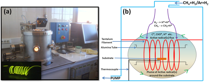
Fig. 1a shows the photograph of our homemade HFTCVD system that was used for the deposition of graphene film on Cu substrate, and the inset shows the alumina tube wound with Ta filament during deposition. Fig. 1b displays the section schematic of our HFTCVD system. Our process cycle for graphene synthesis by HFTCVD can be divided into four stages (see Supplementary Fig. S1).
Figure 1. HFTCVD setup with schematic diagram of graphene growth.
(a) Homemade hot filament thermal CVD set-up for large-area graphene film deposition (inset shows Ta filament (~1800°C) wound around alumina tube. (b) Schematic of graphene growth deposition and formation of active flux of highly charged carbon and hydrogen radicals by catalytic reaction of gaseous precursors with the filament.
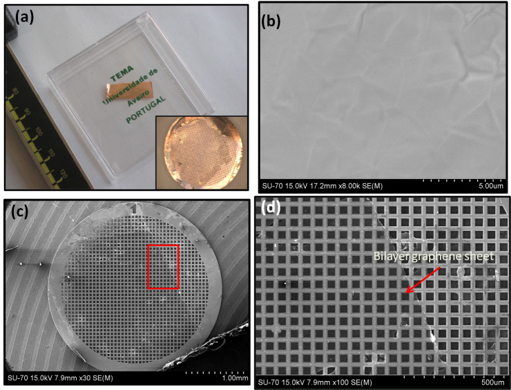
Fig. 2a shows the typical as-deposited monolayer graphene (confirmed by Raman and XPS analysis) sample on Cu foil using our HFTCVD system. The inset in the Fig. 2a shows optical image of the bilayer graphene (BLG) sample transferred on Cu TEM grid. In our work, we have used an aqueous iron (III) chloride (FeCl3) solution (1 M) as an oxidizing etchant to remove the Cu layers, as described elsewhere21. In the present case, we have transferred a BLG, because the pasting of the monolayers deposited on both sides of the Cu substrate takes place during transfer process. Fig. 2b displays a typical field-emission scanning electron microscope (FESEM) image for the as grown graphene films on Cu substrate. Domain regions and wrinkles typical for CVD grown graphene films are observed in our case too22. Fig. 2c displays FESEM image of BLG sheet on Cu grid and Fig. 2d depicts the high magnification FESEM micrograph of the red area denoted in Fig. 2c.
Figure 2. Optical and FESEM images of graphene prepared by HFTCVD.
(a) Large area as-deposited graphene film deposited on Cu substrate (inset shows optical image bilayer graphene transferred on Cu TEM grid). (b) Shows FESEM image for the as grown graphene films on Cu. (c) Shows FESEM image of BLG sheet on Cu grid. (d) Shows high magnification FESEM image for the area denoted in Fig. 2c by red line.
Further, to derive the topographical information and thickness of the as-deposited graphene layers, we employed Atomic Force Microscopy (AFM) in tapping mode on BLG samples transferred to Au/glass and Si substrate (see Supplementary Fig. S2). For image treatment we used specially designed software23. From the AFM topographic results, we can conclude that Au/glass, and Si are probably not the best suited substrates to measure precisely the step height of graphene and, in turn, its thickness due to large surface roughness of base material in agreement with observations of Lui et al.24
To confirm the identity and quality of our as deposited graphene sheets on Cu substrates, we performed detailed micro-Raman studies. Raman spectroscopy is best suited to envisage graphene owing to the observance of distinct and rich vibrational spectra that reveals information related to number of layers, strain, substrate/temperature effects, edge configuration, electronic properties and defects in the graphene structure25.
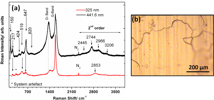
Fig. 3a compares the Raman spectra of graphene sample acquired by excitation at the same point on the sample with 325 nm and 441.6 nm laser lines. The corresponding optical image is shown in Fig. 3b. The Raman spectra were excited using lower power density on the surface to avoid damage. Remarkable changes in the spectrum occur when the energy of excitation decreases from 3.81 eV (325 nm) to 2.81 eV (441.6 nm)26. Within 130–1000 cm−1 spectral region a surprisingly rich spectrum is observed especially, under 441.6 nm (2.8 eV) laser line excitation. We attribute the features observed within this spectral region to the existence of a Cu2O underlayer27, formed between the Cu substrate and graphene layer. Cu2O crystallize in the cuprite structure (space group O4h) and it would expected from group theory: one Raman active phonon (T2g); two Infrared allowed modes (T1u) and three phonons normally nor Raman neither infrared active (IR) modes (T2u, Eu, T2u)28. The spectra presented in Fig. 3a show more phonons bands than that expected from the group theory. This breakdown of the selection rules in Cu2O is long known and is ascribed to defects, nonstoichiometry and due to the resonant exciton29. The attribution of the Raman bands measured in this work in comparison with others previously reported is given in table in supplementary information (see Supplementary Table S6).
Figure 3. Raman spectroscopy of as grown graphene on Cu substrate.
(a) Room temperature Raman spectra of graphene obtained with 325 nm and 441.6 nm laser excitation. (b) Corresponding optical image of as-synthesized graphene on Cu substrate.
The large enhancement observed for the two Raman forbidden (IR allowed) LO phonons localized at 154 cm−1 and 645 cm−1 under 441.6 nm laser line excitation is due to the resonance with the dipole-allowed excitonic states, associated with blue and indigo exciton series, well known in Cu2O28,30.
Next we discuss the region above 820 cm−1 up to 2100 cm−1, wherein the spectra reveal common features, usually observed for graphene such as the G and D peaks, around 1580 and 1350 cm−1, respectively. There is a significant change in the relative intensity of bands D and G, (ID/IG) when the excitation wavelength decreases from of 441.6 nm (2.8 eV) to 325 nm (3.8 eV). We attribute this behavior to a slight displacement on the measuring point resulting from a vibration on the microscope stage when decreasing the laser line. As a consequence, an area with a higher concentration of defects was probed. Moreover, the frequency of G band does not change while the D band shifts (~60 cm−1) to higher frequencies, which agrees with the range 38–70 cm−1/eV reported previously31.
The G peak corresponds to the E2g phonon at the Brillouin-zone center (Γ point), which explains why its position does not change with excitation energy. The D peak is due to the breathing modes of six-atom rings and requires a defect for its activation31,32,33,34. It comes from TO phonons around the K point of the Brillouin zone32,33,34,35 is active by double resonance (DR) intervalley process31 and is strongly dispersive with excitation energy due to a Kohn Anomaly at K Brilouin point36. The presence of D band indicates the presence of a large concentration of defects in graphene. Another aspect that is also evident is the broadening observed under excitation wavelength of 441.6 nm (2.8 eV), and a small shoulder at near ~1620 cm−1.
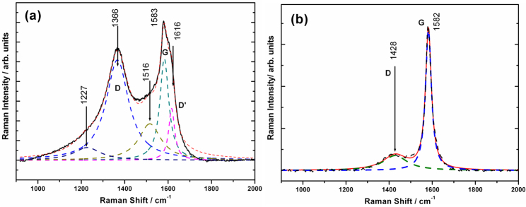
In Fig. 4a,b the spectral region corresponding to D and G bands, for both excitation energies is displayed. A good fit is found when five Lorenztians located at 1227 cm−1, 1366 cm−1 (D), 1516 cm−1, 1583 (G) cm−1 and 1615 cm−1 (D′) are used to deconvolute the Raman spectrum in Fig. 4a. Except the G band (FWHM ~49 cm−1) all the others have larger FWHM, as expected if they are disorder activated. The so-called D′ band has been reported to be originated from DR that occurs as intravalley process2. The bands at 1227 cm−1 and 1516 cm−1, might be related to the phonon frequencies at K and M point of graphite equivalent Brillouin zone31.
Figure 4. Raman spectroscopy of as grown graphene on Cu substrate (in the range 820 cm−1 to 2100 cm−1).
Room temperature Raman spectra of graphene obtained under (a) 441.6 nm and (b) 325 nm laser lines excitation.
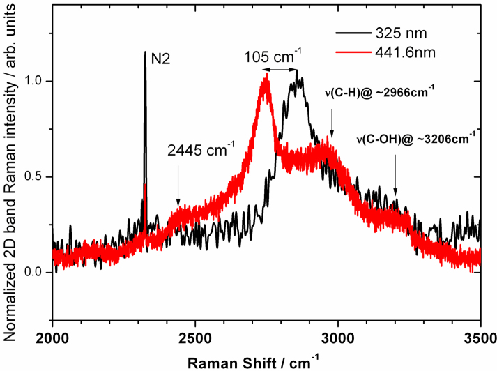
In the case of Fig. 4b only two Lorentzians are required to fit the experimental Raman spectrum viz., the G band at 1582 cm−1 (FWHM ~33 cm−1) and a broader D band at 1428 cm−1 (FWHM ~138 cm−1). Finally, we discuss the spectral region between 2000–3500 cm−1 (Fig. 5), wherein we compare, in the same plot the experimental Raman spectra obtained for both excitation wavelengths. Besides the very narrow peak related with atmospheric molecular nitrogen, we identify the G′ band (2D-band2) of graphene located at 2744 cm−1 and 2852 cm−1 under excitation wavelength of 441.6 nm and 325 nm, respectively. The experimental shift of 109 cm−1 compares well with the range of 92–107 cm−1/eV reported by Irene Calizo et al.37 through Vis-UV region.
Figure 5. Raman spectroscopy of as grown graphene on Cu substrate (in the range 2000 cm−1 to 3500 cm−1).
Comparison of room temperature Raman spectra of graphene obtained under 325 nm and 441.6 nm laser excitation lines within 2D band region.
In highly quality graphene layer prepared by micromechanical cleavage of highly orientated pyrolytic graphite and transferred onto SiO2/Si the most prominent feature is the G′ band, even when no D peak is present, since no defects are required for the activation of second order phonons37. Moreover, under visible wavelength excitations the G′ is a sharp single peak in graphene in contrast with graphite or few-layers graphene37,38,39. This phonon band originates from intervalley scattering of two in plane transverse optical (iTO) phonons along the Γ-K-M-K'-Γ in the first Brilouin zone38.
Fig. 3 also shows that, in contrarily to highly quality graphene39, the G band is the more pronounced peak under both ultraviolet excitation (325 nm) and visible excitation (441.6 nm). Irene Calizo et al.37 also found that the graphene's G peak remains pronounced under UV (325 nm) and visible excitation (441.6 nm), however in that case they observed that the G′ band intensity undergoes a severe quenching. In the present work the IG′/IG only slightly decreases under ultraviolet excitation when compared with visible excitation.
Fig. 5 shows the Raman spectra for both wavelength excitations, after normalized to G′ peak Raman Intensity. Inspite of the lower signal/noise ratio we can identify two Raman bands at ~2966 cm−1 and ~3206 cm−1 that don't shift with the wavelength excitation. The absence of the dispersive character and their spectral location indicates that these bands are most probably related with the sp2 C-H and sp3 C-H stretching vibrations and C-OH stretching vibration, respectively. Under excitation wavelength of 441.6 nm, beyond the G′ band a weak band around 2445 cm−1 is also visible. This band is located very close to the reported G* band26, which also originate from a DR intervalley process, but that involves one iTO and one longitudinal acoustic phonon35. It is interesting to note that for both excitation wavelengths the G′ band shape has close resemblance to the G′ band shape usually observed for monolayer graphene, than the one obtained for a bilayer graphene or bulk graphite38. The low intensity of G′ band can be attributed to the presence of defect related D band.
Additionally, to corroborate the Raman findings, prove the existence of monolayer graphene and envisage the oxygen content along with the functional groups on the as-grown and transferred graphene samples we further performed detailed X-ray photoelectron spectroscopy (XPS) studies.
XPS is a suitable technique for determining the chemical composition of carbonaceous samples because the binding energy of a core level peak contains not only elemental, but also the chemical information. Moreover, the well determined binding energy for C 1s in sp2 configuration (284.8 eV) makes this technique a valuable methodology to evaluate charge transfer process inside a molecule or material40,41.
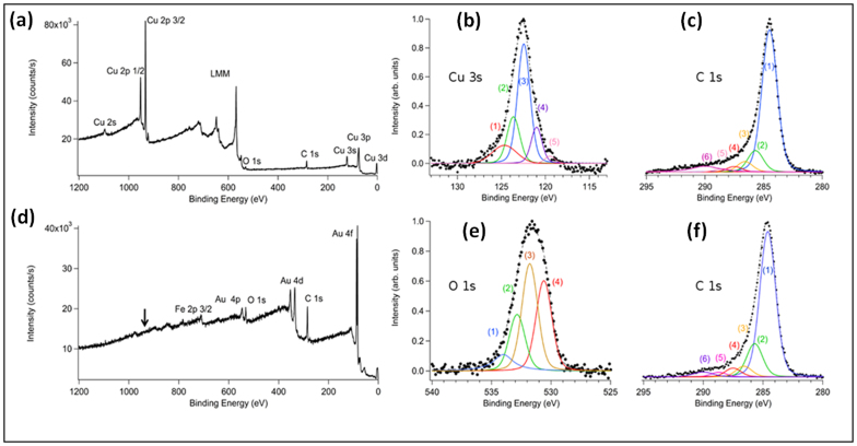
A core level peak can be decomposed in different curve components and each of them is signature of the chemical/electronic environment of the element41. Fig. 6a shows an overview XPS scan for the as deposited graphene films on Cu substrate. As expected the presence of copper, oxygen and carbon is evident in the general spectra. Moreover from the relative intensities between the Cu (substrate) and C (overlayer) we can estimate the number of layers of the adsorbate41. This intensity analysis is compatible with a monolayer graphene sheet on the surface (θ = 0.94 ML). Fig. 6b,c depicts the high-resolution XPS scans for Cu 3s and C 1s, respectively. Fig. 6c shows the C 1s high resolution XPS scan for the graphene grown on a copper substrate via our HFTCVD. The peak can be decomposed in six components corresponding to C sp2, C-OH, C-O, C = O, C-C = O, and O-C = O with respective binding energies of 284.6 (component 1 in Fig. 6b), 285.7 (component 2) (2), 286.6 (3), 287.5 (4), 288.7 (5) and 290 eV (6), respectively40.
Figure 6. X-ray photoelectron spectroscopy of as-synthesized graphene by HFTCVD.
(a) General scan for the as-grown graphene on copper (G/Cu). (b) High-resolution XPS scan for Cu 3s core level peak. (c) High-resolution XPS scan for the C 1s core level peak of G/Cu. (d) General scan for the transferred graphene on a gold-coated silica substrate. Au, C, O and Fe (impurities) peaks are the main features of the spectra. Small arrow indicates the position of the Cu 2p core level. (e) High-resolution XPS scan for the O 1s core level peak of the transferred sample. (f) High-resolution XPS scan for the C 1s core level peak of the transferred sample. All the detailed core level peaks, b), c), e) and f), have been decomposed into curve components, shown underneath the experimental data points. The curve that overlaps the data points corresponds to the best fit.
The oxygen-related components of the decomposed peak in curve components correspond to 27.7% of the total area of the C 1s peak indicating a certain degree of oxidization, which most likely could have come from the low-vacuum in the growth chamber. On the other hand, Fig. 6b shows the high resolution spectra for Cu 3s. The choice of this particular peak is due to the regular (flat) background that surrounds this core level, making the Cu 3s perfectly suitable for peak decomposition in curve-components, unlikely to other more intense levels of Cu. The Cu 3s spectrum can be deconvoluted into five peaks at 119.5 (1), 121.0 (2), 122.4 eV (3), 123.6 (4) and 124.7 (5) that could be assinged to Cu = C, Cu-C, Cu-Cu, Cu-O and Cu-OH, respectively42,43,45.
In any case, the need of including core-level components in the fit with binding energies different to 122 eV (component 3 Fig. 6b) indicates the presence of CuO at the surface region42. However, it should be well-remembered that XPS is not the best probe to distinguish between different oxidation states of Cu due to the small energy shifts between the different oxidized configurations. For instance, both Cu2O and the main Cu-Cu component have been reported to appear around 122.2 eV42; hence, we believe that the main oxide should correspond to Cu2O as confirmed by the Raman studies.
Fig. 6d shows an overview scan for the graphene transferred to Au. As expected, in the spectrum the peaks corresponding to Au are present while those pertaining to Cu are completely absent. The position where Cu 2p is expected is pointed by a small arrow. Presence of Fe on the surface, coming from impurities of the FeCl3 solution used in the transferring process, is insignificant (normalized ratio Fe 3p/C 1s is 0.025). There are no detectable traces of Cl on the surface. Fig. 6e,f depicts the O 1s and C 1s high-resolution XPS scans for the graphene sample transferred on Au substrate, respectively.
The C 1s spectra for both the transferred as well as for the as-grown virgin sample on Cu substrate look similar eradicating the possibility of any strong chemical modification during the transfer process. The high resolution scan for C 1s on Au substrate shows peaks at the same energies of Fig. 6c, that is at 284.6 (1), 285.7 (2), 286.6 (3), 287.5 (4), 288.7 (5), 290 (6) eV and can be correlated to carbon atoms in the following configurations C sp2, C-OH, C-O, C = O, O = C,C-C = O and O-C = O, respectively. On transfer, C bonded with O components slightly increases, from the original 27.7% to 31.5%, indicating a small oxidization during the process but no strong modification in the chemical configuration of the transferred layers.
By comparing the intensities within the Fig. 6d we can estimate the number of transferred graphene layers; from the normalized ratio (intensities divided by the cross section) between intensities C 1s/Au 4f = 5.04. This value is compatible with the transfer of about 2.6 ML, as it can be also confirmed by optical microscope images (see Supplementary Fig. S2a). However, it should be remembered that the clean Au-coated silica samples used as substrate have carbon contaminants. The normalized C 1s/Au 4f ratio is 0.75 for the clean samples which correspond to θ = 0.7 ML. By subtracting both quantities, we conclude to have transferred a bilayer of graphene (BLG, 1.9 ML) on to Au substrate. Formation of bilayer is obvious as graphene monolayers deposited on both sides of Cu substrates get pasted as a result of Cu dissolution in the FeCl3 solution during the transfer process. Further, the formation of bilayer graphene is also confirmed by fast Fourier transform (FFT) pattern of high resolution transmission electron micrographs (HRTEM) of transferred graphene films (see Supplementary Fig. S3).
The presence of carbon-oxygen bonding is also evident in the O 1s spectrum recorded on graphene transferred to Au substrate (Fig. 6e). The O 1s spectrum shows peaks at 534 (1), 532.9 (2), 531.8 (3) and 530.6 (4) eV, respectively, which could be assigned to C-C = O/O-C = O, C-OH/C-O, hydroxides, C = O and other carbon complexes43,44,45. The O 1s spectrum indicates that majority of oxygen is present in the form of hydroxides. It should be remembered that oxygen plays a pivotal role in introducing a finite energy gap in the graphene structure46. Huang et al.47 reported bandgap to be a non-monotonic function of the O 1s/C 1s ratio, with minima at O 1s/C 1s = 0.11 and 0.25, corresponding to bandgap values of 0.780 eV and 0.354 eV, respectively. In our sample (Graphene/Cu), the normalized ratio O 1s/C 1s is 0.15 indicating that the graphene grown on copper is slightly oxidized both in the growth and transfer process with bandgap value that theoretically47 lies between 0.780 to 0.354 eV. The normalized ratio of O 1s/C 1s is similar to the value for reduced-GOx (graphene oxide) samples (which is normally about 0.1). Noting that GOx samples normally have O 1s/C 1s ratio ~140, we conclude that the resulting product can be seen as a partially oxidized graphene sheet.
To envisage the structure-conductance relationship, we performed detailed Conductive Atomic Force Microscopy (C-AFM) in contact mode, which provided simultaneously topographic and local electronic information48 of the free standing bilayer graphene (BLG) membrane on TEM copper grid. Copper grids were chosen as substrates for current imaging because they permit direct observation of inherent local electronic properties of BLG membranes in free standing state without substrate effects. C-AFM can be done at ambient conditions and provides a high contrast due to contact resistance difference between the tip and the sample. It is very advantageous over UHV-STM that is relatively painstaking and lateral force microscopy (LFM) wherein quantitative analysis is difficult owing to crosstalk between topographic and LFM signals49. C-AFM also provides a straightforward means of studying local electronic properties at grain boundaries and near wrinkles in addition to electrical discontinuities from micro to nano level50. The complete knowledge into these local current path variations is a prerequisite to use these BLG sheets as transparent conductive electrodes and chemical or biological sensors22.
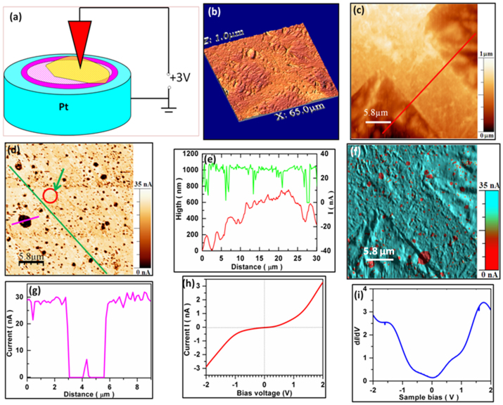
Fig. 7a shows schematics of the C-AFM current mapping measurement setup used in the present experiment for freely suspended BLG sheet on TEM copper grid and Fig. 7b shows large-area 3D topographic image for the same. While Fig. 7c shows topography of freely suspended BLG membrane and the corresponding local current image is shown in Fig. 7d. The non-conducting regions are clearly seen as dark patches in the film.
Figure 7. Local current mapping of free-standing graphene membrane on TEM Cu grid.
(a) Schematic of a conductive AFM measurement freely suspended BLG sheet on TEM copper grid in contact mode. (b) AFM topography of large area suspended BLG membrane in contact mode. (c,d) Shows AFM topography of suspended BLG membrane and the corresponding current image with sample bias voltage +3 V DC. (e) Height profile and current measurement along the red line (Fig. 7c) and green line (Fig. 7d), respectively. (f) Shows a combined current and topography image wherein the conducting domain is represented by green color and non-conducting areas are seen as red spots. (g) Shows current plots along the line (indicated by pink color in Fig. 7d). (h,i) Shows local point contact I–V measurement and corresponding dI/dV curve performed on the red circle region (indicated by green arrow in Fig. 7d).
To confirm the same, we performed current measurements on a large area of the BLG and a single patch as depicted by the straight line (Pink) in Fig. 7d. Fig. 7e shows the height vs. distance and distance vs. current plot for the straight line (Green) in Fig. 7d, wherein, the dips in the green line clearly indicate that the film is composed of regular non-conducting domains in the conducting graphene sheet. The red line in Fig. 7e represents the height profile for the straight line region in Fig. 7c. The convolutions (Fig. 7e) in the height profile arise as the membrane is freely suspended on the grid.
Fig. 7f represents a combined current and topography image wherein the conducting domain is represented by green color and non-conducting areas are seen as red spots. The presence of small irregular sized non-conducting patches within BLG is clearly evident. Fig. 7g displays the current distance curve for dark patch shown by pink line in Fig. 7d. One can clearly see the current becomes almost zero on the patch and regains when the tip is on the conducting one. The local current-voltage (I–V) curve shown in Fig. 7h and dI/dV curve in Fig. 7i corresponds to the point contact measurement depicted by red circle in Fig. 7d. The metallic signature for the BLG sample is clearly evident. Such kind of behavior was also observed by Liang et al. during kelvin probe measurements on functionalized graphene sheet51. The presence of non-conducting domains as evinced by C-AFM measurements can be related to the occurrence of hydroxyl and oxygenated functional groups observed in Raman and XPS studies thereby indicating slightly oxidized graphene.
Discussion
By corroborating the experimental approach with Raman, XPS, AFM analysis a probable mechanism can be putforth for the growth of graphene films by HFTCVD system. It should be well-remembered that there is always a thermodynamic driving force for deposition of graphitic phase under conditions of diamond deposition as graphite is more stable phase than diamond9. In our methodology, there is a steady state flow of primary, secondary and tertiary active radicals formed due to; (a) cracking of gases on the filament, (b) catalytic reaction of the filament, (c) reaction among the radicals themselves52. When the filament is on, high hydrogen diffusion and low carbon solubility in Cu53 accompanied by atomic hydrogen etching of carbon precludes any deposition on the Cu substrate12. The largely negatively charged plume of radicals is in constant equilibrium as long as the filament is on12. A gradient in gas composition and gas flow rate is created by placing of the substrate inside the alumina tube20. The presence of charged gas phase nuclei in thin film processing by HFCVD has already been established12.
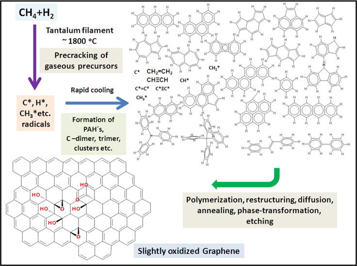
As soon as, the filament is put-off with concomitant replacement of CH4 by Ar, the temperature of the system starts to drop with perhaps supersaturation, polymerization, diffusion, restructuring, annealing, etching and phase transformation of (i) atomic carbon species, (ii) small gas phase carbon clusters, (iii) polyaromatic hydrocarbons (PAH's) near the surface thereby forming a graphene monolayer on the Cu surface (Fig. 8). The Ar/H2 flow not only helps in flushing the excess active species and amorphous carbon thereby preventing unintended carbon deposition, but also anneals the film to some extent.
Figure 8. Probable mechanism of Graphene growth by HFTCVD.
Schematic illustration of various physicochemical processes and intermediates during graphene growth by HFTCVD technique.
We believe that the conventional nucleation on Cu substrate is avoided due to precracking of gases on the Ta filament and the positioning of the Cu substrate in the filament. Formation of graphene on Cu by C2 radicals has been reported previously by PECVD54. Also, the presence of copper(I)oxide as revealed by Raman and XPS studies excludes the probability of nucleation on Cu. The presence of copper oxide(s) along-with graphene was also reported by Hesjedal et al. during continuous roll-to-roll growth of graphene55. Qi et al.56 also reported the formation of microsized CuO islands on graphene films due to ambient oxidation of underlying copper that is exposed via polygonal holes created in the graphene film during H2 cooling. The graphene films deposited by us are pinhole free without any overlaying deposition of copper oxide(s) as revealed by FESEM analysis (Fig. 2b–d). Prima-facie the concomitant presence of Cu2O may be attributed to presence of residual oxygen present in the system.
Further, this residual oxygen doping must also have played a pivotal role in oxidation of dangling bonds in our graphene films as evinced by presence of carbon-oxygen bonds in XPS and Raman studies8. To test our hypothesis we also tried deposition on Ni and SiO2/Si substrates (see Supplementary Fig. S4,S5). Graphene deposition was observed on both the substrates but the quality of graphene films grown on Ni was far superior when compared to that grown on Cu and SiO2/Si. This indicates that the substrate plays important role in determining the quality of the graphene films and hence the name given to the method.
In our technique, it is possible to deposit samples at low temperatures as precracking of gaseous precursors occurs on the Ta filament6. In lieu with this premise, we were able to observe graphene growth on Cu substrates at ~300°C and also 0% H2 dilution of CH4 (results not shown). We would like to specially mention that no graphene growth was observed under conventional HFCVD with different substrate positions and gas ratios, in contrast to the only report by Stojanovic et al.14
We have demonstrated hot filament thermal CVD (HFTCVD) a new hybrid CVD process combining best traits of HF and thermal CVD to fabricate graphene films as proof of the concept. Strictly monolayer graphene films grown on Cu substrates were studied in detail. Raman and XPS analysis showed the presence of hydroxyl and oxygenated functional groups thereby indicating slight oxidization of the as grown graphene films. C-AFM measurements revealed the presence of non-conducting domains that can be correlated to the occurrence of hydroxyl and oxygenated functional groups observed in Raman and XPS studies. C-AFM also confirmed the metallic nature of our bilayer graphene films. We believe that HFTCVD can be further extended to dope graphene with heteroatoms (H, N, B, etc.,) and combine graphene with wide variety of functional materials like diamond for intended applications. In principle, HFTCVD is not only applicable for graphene, but also can be extended to all other functional materials and processes possible by HFCVD and thermal CVD on industrial scale.
Methods
Preparation of monolayer graphene sheet by HFTCVD
A homemade HFTCVD system (Fig. 1a) was used to grow graphene on Cu (GoodFellow, thickness 0.025 mm, purity 99.9%), Ni (GoodFellow, thickness 0.025 mm, purity 99.9%) and SiO2 (300 nm)/Si (p-type, Crystal GmbH). The substrates were cleaned by sonication in organic solvents (acetone and isopropanol) prior to the loading in the CVD chamber. In our HFTCVD system, Ta filament was used (Advent Research Materials, diameter ~0.40 mm, purity ~99.9%), and substrates were placed in the middle of alumina tube (Frialit-Degussit Technical Ceramics, diameter ~2 cm, length ~8 cm). All precursors gases (CH4, H2 and Ar) with purity ~99.99% from Praxair and Air Liquide were used for graphene deposition.
Characterization of graphene sheet by AFM and FESEM
Two commercial AFM (NT-MDT, Ntegra Aura and Nanotec's AFM with Dulcinea Electronic) were used for surface topography studies on as-grown and transferred graphene films in tapping mode. In addition to this, field-emission scanning electron microscope (FESEM; SU-70, JEOL) was used to study surface morphology of as-grown graphene on Cu substrate and graphene samples transferred on TEM Cu grid (Ted Pella Inc.).
Characterization of graphene sheet by X-ray photoelectron spectroscopy (XPS)
XPS spectra were acquired in an ultra high vacuum equipment (~10−10 mbar)40,57,58 using a hemispherical electron energy analyzer and an Mg K-alpha X-ray source (1253.6 eV). The XPS spectra of the different regions were decomposed in lorentzian-gaussian curve components. We applied the criterion of using the lowest number of components with widths smaller than 1.5 eV for the analysis of the O 1s and C 1s peaks. All samples were measured under the same conditions and fitted with the same parameters.
Characterization of as-deposited graphene sheet on Cu substrate by Raman spectroscopy
The Raman spectra were obtained at room temperature in back scattering configuration with a Jobin-Yvon LabRam HR equipped with a Multichannel air cooled (−70°C) CCD detector. An objective of 50x magnification was used to focus on the sample surface when excited with the 325 nm and 441.6 nm laser lines, respectively. The Raman spectra were excited using lower power density on the surface to avoid damage or laser induced heating. Preliminary measurements were carried out in order to optimize the power density and the signal/noise ratio for which the Raman spectra remain unchanged for sequentially acquisitions in the same spot. The system was calibrated at 520 cm−1 and 1332 cm−1 using a Si (111) and diamond reference samples, under 325 nm laser excitation lines. The laser line was changed to 441.6 nm, maintaining the focus at the same point on the sample. The calibration was attained using the Raman band at 2324 cm−1, which is assigned to the Q-branch of the fundamental vibration-rotation of N2 atmospheric gas59 that fortunately is detected in Raman spectrum collected under both laser lines excitation.
Local current mapping of free-standing graphene membrane on TEM Cu grid
Local current mapping was performed by conductive atomic force microscopy (C-AFM) (NT-MDT, Ntegra Aura) in contact mode under ambient conditions. The C-AFM involves contact-mode Pt/Ir-coated silicon cantilevers (spring constant ~0.2 N/m, resonance frequency ~300 kHz, CSG10/Pt, NT-MDT) for local current mapping and surface imaging. The topography and current imaging of BLG sheet was recorded simultaneously with bias voltage +3 V DC. During C-AFM measurements, a force of 200 nN was maintained; the tip was electrically grounded, and a bias voltage was applied to the sample. Tip velocities of 2–10 µm/s were used for C-AFM imaging, while I–V measurements were recorded when sample was biased with ±3 V DC supply (Fig. 7a).
High-resolution transmission electron microscopy of transferred graphene sheets
A conventional high-resolution (HR) TEM (JEOL 2200F TEM/STEM) was operated at 200 kV with a point resolution of 0.16 nm, equipped with a GIF-2000 spectrometer on graphene films transferred on Cu TEM grid (Ted Pella Inc.) by dissolution of Cu substrates.
Author Contributions
M.K.S. conceived and directed the research. M.K.S. designed and developed the HFTCVD system for graphene growth. The graphene deposition work were carried out by R.H. & M.K.S. XPS, Raman, AFM, C-AFM, HRTEM, analysis were carried out by P.M., M.R.C., I.B., M.K.S., R.H., J.G., J.M., J.A.M.G. All authors participated equally in discussions, analysis of the results and towards writing of the manuscript.
Supplementary Material
Supplementary Information for Large-area high-throughput synthesis of monolayer graphene sheet by Hot Filament Thermal Chemical Vapor Deposition
Acknowledgments
This research work was supported by the grant received by Manoj Kumar Singh from FCT (Grant No. PTDC/CTM-NAN/121108/2010), Ministry of Science and Technology, Portugal. Ranjit Hawaldar expresses his gratitude to FCT for supporting through Postdoctoral Grant SFRH/BPD/79016/2011. The author M.R Correia thanks the financial support from FCT (Grant No. PEst-C/CTM/LA0025/2011). Grants from the Spanish administration CSD2007-41, MAT2011-534 are also acknowledged. P M acknowledges financial support by the “Rafael Calvo Rodes”, scholarship program.
References
- Bonaccorso F., Sun Z., Hasan T. & Ferrari A. C. Graphene photonics and optoelectronics. Nature Photon 4, 611–622 (2010). [Google Scholar]
- Ferrari A. C. et al. A. K. Raman Spectrum of Graphene and Graphene Layers. Phys. Rev. Lett. 97, 187401 (2006). [DOI] [PubMed] [Google Scholar]
- Geim A. K. & Novoselov K. S. The rise of graphene. Nature Mater. 6, 183–191 (2007). [DOI] [PubMed] [Google Scholar]
- Choi W., Lahiri I., Seelaboyina R. & Kang Y. Synthesis of Graphene and Its Applications: A Review. Crit Rev Solid State Mater Sci. 35, 52–71 (2010). [Google Scholar]
- Batzill M. The surface science of graphene: Metal interfaces, CVD synthesis, nanoribbons, chemical modifications, and defects. Surf.Sci.Rep. 67, 83–115 (2012). [Google Scholar]
- Wang Y. et al. Toward High Throughput Interconvertible Graphane-to-Graphene Growth and Patterning. ACS Nano 4, 6146–6152. (2010). [DOI] [PubMed] [Google Scholar]
- Henry M. et al. Metal-Free Growth of Nanographene on Silicon Oxides for Transparent Conducting Applications. Adv. Funct. Mater. 22, 2123–2128 (2012). [Google Scholar]
- Takami T. et al. Y. Catalyst-Free Growth of Networked Nanographite on Si and SiO2 Substrates by Photoemission-assisted Plasma-enhanced Chemical Vapor Deposition. e-J. Surf. Sci. Nanotech. 7, 882–890 (2009). [Google Scholar]
- Song H. J. et al. Large scale metal-free synthesis of graphene on sapphire and transfer-free device fabrication. Nanoscale. 4, 3050–3054 (2012). [DOI] [PubMed] [Google Scholar]
- Kim Y. et al. Low-temperature synthesis of graphene on nickel foil by microwave plasma chemical vapor deposition. Appl. Phys. Lett. 98, 263106 (2011). [DOI] [PMC free article] [PubMed] [Google Scholar]
- R.E.I. Schropp. Frontiers in HWCVD. Thin Solid Films. 517, 3415–3419 (2009). [Google Scholar]
- Hwang N. M. & Lee D. K. Charged nanoparticles in thin film and nanostructure growth by chemical vapour deposition. J. Phys. D: Appl. Phys 43, 483001 (2010). [Google Scholar]
- Subramani K. & Ahmed W. Emerging Nanotechnologies in Dentistry: Processes, Materials and Applications Elsevier, Micro and Nanotechnology series (Chapter 15, page number 246, ISBN: 978-1-4557-7862-1).
- Stojanović D., Woehrl N. & Buck V. Synthesis and characterization of graphene films by hot filament chemical vapour deposition. Phys. Scr. T149, 014068 (2012). [Google Scholar]
- Bakr N. A. et al. Influence of deposition pressure on structural, optical and electrical properties of nc-Si:H films deposited by HW-CVD. J. Phys. Chem. Solids. 72, 685–691 (2011). [Google Scholar]
- Funde A. M. et al. Influence of hydrogen dilution on structural, electrical and optical properties of hydrogenated nanocrystalline silicon (nc-Si:H) thin films prepared by plasma enhanced chemical vapour deposition (PE-CVD). Sol. Energy Mater. Sol. Cells. 92, 1217–1223 (2008). [Google Scholar]
- Cojocaru C. S., Larijani M., Misra D. S., Singh M. K., Veis P. & Le Normand F. A new polarised hot filament chemical vapor deposition process for homogeneous diamond nucleation on Si(100). Diamond Relat. Mater. 13, 270–276(2004). [Google Scholar]
- Misra D. S. et al. Melting and defect generation in chemical vapor deposited diamond due to irradiation with 100 MeV Au+ and Ag+ ions. Thin Solid Films 503, 121–126 (2006). [Google Scholar]
- Madaleno J. C., Singh M. K., Titus E., Cabral G., Grácio J. & Pereira L. Electron field emission from patterned nanocrystalline diamond coated α-SiO2 micrometer-tip arrays. Appl. Phys. Lett. 92, 023113 (2008). [Google Scholar]
- Zhang Yi., Zhang L., Kim P., Ge M., Li Z. & Zhou C. Vapor Trapping Growth of Single-Crystalline Graphene Flowers: Synthesis, Morphology, and Electronic Properties. Nano Lett. 12(6), 2810–2816 (2012). [DOI] [PubMed] [Google Scholar]
- Kim K. S. et al. Large-scale pattern growth of graphene films for stretchable transparent electrodes. Nature, 457, 706–710 (2009). [DOI] [PubMed] [Google Scholar]
- Ahmad M., Han S. A., Tien D. H., Jung J. & Seo Y. Local conductance measurement of graphene layer using conductive atomic force microscopy. J. Appl. Phys. 110, 054307 (2011). [Google Scholar]
- orcas I., Fernández R., Gómez-Rodríguez J. M., Colchero J., Gómez-Herrero J. & Baro A. M. WSXM: software for scanning probe microscopy and a tool for nanotechnology. Rev. Sci. Instrum. 78, 013705 (8 pages) (2007). [DOI] [PubMed] [Google Scholar]
- Lui C. H., Liu Li., Mak K. F., Flynn G. W. & Heinz T. F. Ultraflat Graphene. Nature 462, 339–341 (2009). [DOI] [PubMed] [Google Scholar]
- Stadler J., Schmid T. & Zenobi R. Nanoscale chemical imaging of single-layer graphene. ACS Nano 5(10), 8442–8448 (2011). [DOI] [PubMed] [Google Scholar]
- Mafra D. L. et al. Determination of LA and TO phonon dispersion relations of graphene near the Dirac point by double resonance Raman scattering. Phys Rev. B. 76, 233407 (4 pages) (2007). [Google Scholar]
- Reimann K. & Syassen K. Raman scattering and photoluminescence in Cu2O under hydrostatic pressure. Phys. Rev B. 39, 11113–11119 (1989). [DOI] [PubMed] [Google Scholar]
- Francesco Biccari. Defects and Doping in Cu2O, Ph. D. Thesis. Sapienza – University of Rome, (2009). [Google Scholar]
- Powell D., Compaan A., Macdonald J. R. & Forman R. A. Raman-scattering study of ion-implantation-produced damage in Cu2O. Phys. Rev. B. 12, 20–25 (1975). [Google Scholar]
- Williams P. F. & Porto S. P. S. Symmetry-Forbidden Resonant Raman Scattering in Cu2O. Phys. Rev. B. 8, 1782–1785 (1973). [Google Scholar]
- Thomsen C. & Reich S. Double Resonant Raman Scattering in Graphite. Phys. Rev. Lett. 85, 5214–5217 (2000). [DOI] [PubMed] [Google Scholar]
- Ferrari A. C. & Robertson J. Interpretation of Raman spectra of disordered and amorphous carbon. Phys. Rev. B. 61, 14095–14107 (2000). [Google Scholar]
- Ferrari A. C. & Robertson J. Resonant Raman spectroscopy of disordered, amorphous, and diamondlike carbon. Phys. Rev. B. 64, 075414 (13 pages) (2001). [Google Scholar]
- Tuinstra F. & Koenig J. L. Raman Spectrum of Graphite. J. Chem. Phys. 53, 1126–1130 (1970). [Google Scholar]
- Maultzsch J., Reich S. & Thomsen C. Double-resonant Raman scattering in graphite: Interference effects, selection rules, and phonon dispersion. Phys Rev B. 70, 155403 (9 pages) (2004). [Google Scholar]
- Piscanec S., Lazzeri M., Mauri F., Ferrari A. C. & Robertson J. Kohn Anomalies and Electron-Phonon Interactions in Graphite. Phys. Rev. Lett. 93, 185503 (4 pages) (2004). [DOI] [PubMed] [Google Scholar]
- Calizo I., Bejanari I., Rahman M., Liu G. & Balandin A. A. Variable temperature Raman microscopy as a nanometrology tool for graphene layers and graphene-based devices. J. Appl. Phys. 106, 043509 (3 pages) (2009). [Google Scholar]
- Cançado L. G., Reina A., Kong J. & Dresselhaus M. S. Geometrical approach for the study of G′ band in the Raman spectrum of monolayer graphene, bilayer graphene, and bulk graphite. Phys Rev. B. 77, 245408 (2008). [Google Scholar]
- Gupta A., Chen G., Joshi P., Tadigadapa S. & Eklund P-C. Raman Scattering from High-Frequency Phonons in Supported n-Graphene Layer Films. Nano Lett. 6(12), 2667–2673 (2006). [DOI] [PubMed] [Google Scholar]
- Castelaín M. et al. Graphene Functionalisation with a Conjugated Poly(fluorene) by Click Coupling: Striking Electronic Properties in Solution. Chem. Eur. J. 18, 4965–4973 (2012). [DOI] [PubMed] [Google Scholar]
- Ertl G. & Kuppers J. Low Energy Electrons and Surface Chemistry, Wiley-VCH Verlag GmbH, 2nd edition, (1986).
- McIntyre N. S. & Cook M. G. X-Ray Photoelectron Studies on Some Oxides and Hydroxides of Cobalt, Nickel and Copper. Anal. Chem. 47, 2208–2213 (1975). [Google Scholar]
- Lim A. S. & Atrens A. ESCA studies of nitrogen-containing stainless steels. Appl. Phys. A-Mater, 51, 411–418 (1990). [Google Scholar]
- Yang D. et al. Chemical analysis of graphene oxide films after heat and chemical treatments by X-ray photoelectron and Micro-Raman spectroscopy. Carbon 47, 145–153 (2009). [Google Scholar]
- Rosenthal D., Ruta M., Schlögl R. & Minsker L. K. Combined XPS and TPD study of oxygen-functionalized carbon nanofibers grown on sintered metal fibers. Carbon. 48, 1835–1843. (2010). [Google Scholar]
- Nourbakhsh A. et al. Bandgap opening in oxygen plasma-treated graphene. Nanotechnology. 21, 435203 (2010). [DOI] [PubMed] [Google Scholar]
- Huang H., Li Z., She J. & Wang W. Oxygen density dependent band gap of reduced graphene oxide. J. Appl Phys. 111, 054317 (2012). [Google Scholar]
- Otsuka Y., Naitoh Y., Matsumoto T. & Kawai T. Point-contact current-imaging atomic force microscopy: Measurement of contact resistance between single-walled carbon nanotubes in a bundle. Appl. Phys. Lett. 82, 1944 (2003). [Google Scholar]
- Kellar J. A., Alaboson J. M. P., Wang Q. H. & Hersam, M. C. Identifying and characterizing epitaxial domains on partially graphitized SiC(0001) surfaces using scanning probe microscopy. Appl. Phys. Lett. 96, 143103 (2010). [Google Scholar]
- Mativetsky J. M. et al. Local Current Mapping and Patterning of Reduced Graphene Oxide. J. Am.Chem.Soc. 132(40), 14130–14136 (2010). [DOI] [PubMed] [Google Scholar]
- Yan L., Punckt C., Aksay I. A., Mertin W. & Bacher G. Local Voltage Drop in a Single Functionalized Graphene Sheet Characterized by Kelvin Probe Force Microscopy. Nano Lett. 11, 3543–3549 (2011). [DOI] [PubMed] [Google Scholar]
- Adhikari S., Viswanathan N. N. & Dusane R. O. Thermodynamic analysis of gas phase chemistry in hot wire chemical vapor deposition of a-Si:H and μc-Si:H. Journal of Non-Crystalline Solids 352(9-20), 928–932 (2006). [Google Scholar]
- Mattevi C., Kim H. & Chhowalla M. A review of chemical vapour deposition of graphene on copper. J. Mater. Chem. 21, 3324–3334 (2011). [Google Scholar]
- Terasawaa T. & Saiki K. Growth of Graphene on Cu by Plasma Enhanced Chemical Vapor Deposition. Carbon. 50(3), 869–874 (2011). [Google Scholar]
- Hesjedal T. Continuous roll-to-roll growth of graphene films by chemical vapor deposition. Appl. Phys. Lett. 98, 133106 (3 Pages) (2011). [Google Scholar]
- Qi Y., Eskelsen J. R., Mazur U. & Hipps K. W. Fabrication of graphene with CuO islands by chemical vapor deposition. Langmuir 28(7), 3489–3493 (2012). [DOI] [PubMed] [Google Scholar]
- Otero G. et al. Fullerenes from aromatic precursors by surface-catalysed cyclodehydrogenation. Nature 454, 865–868 (2008). [DOI] [PubMed] [Google Scholar]
- Mendez J., López M. F. & Martín-Gago, J. A. On-surface synthesis of cyclic organic molecules. Chem. Soc. Rev. 40(9), 4578–4590 (2011). [DOI] [PubMed] [Google Scholar]
- Tuma R., Vhoník S., Li H. & Thomas G. J. Jr. Cysteine conformation and sulfhydryl interactions in proteins and viruses. 3. Quantitative measurement of the Raman S-H band intensity and frequency. Biophysical Journal 65, 1066–1072 (1993). [DOI] [PMC free article] [PubMed] [Google Scholar]
Associated Data
This section collects any data citations, data availability statements, or supplementary materials included in this article.
Supplementary Materials
Supplementary Information for Large-area high-throughput synthesis of monolayer graphene sheet by Hot Filament Thermal Chemical Vapor Deposition


