

Abstract
Reliability, scalability and clinical viability are of utmost importance in the design of wireless Brain Machine Interface systems (BMIs). This paper reports on the design and implementation of a neuroprocessor for conditioning raw extracellular neural signals recorded through microelectrode arrays chronically implanted in the brain of awake behaving rats. The neuroprocessor design exploits a sparse representation of the neural signals to combat the limited wireless telemetry bandwidth. We demonstrate a multimodal processing capability (monitoring, compression, and spike sorting) inherent in the neuroprocessor to support a wide range of scenarios in real experimental conditions. A wireless transmission link with rate-dependent compression strategy is shown to preserve information fidelity in the neural data. At 32 channels, the neuroprocessor has been fully implemented on a 5mm×5mm nano-FPGA, and the prototyping resulted in 5.19 mW power consumption, bringing its performance within the power-size constraints for clinical use. The optimal design for compression and sorting performance was evaluated for multiple sampling frequencies, wavelet basis choice and power consumption.
Keywords: Brain machine interfaces, data reduction, low power, nano-FPGA, neural recording microsystem, neuroprocessor, spike sorting, wireless telemetry
I. Introduction
Large scale ensemble recordings with penetrating microelectrode arrays have been shown to yield affluent information content about motor intent in subjects with severe motor and communication deficits [1-3]. One major obstacle that precludes the extraction of this pristine information in awake, behaving subjects is the need to be tethered to large size recording equipment that are typically found in laboratory settings. Clinical viability, however, requires developing fully implantable and wireless neural recording microsystems capable of optimizing the power consumption and data bandwidth without compromising the information in the neural activity, thereby enabling the subject to interact freely with the surrounding and minimize any risk of infection and discomfort.
Wireless neural recording system design has been the community trend in a number of labs in recent years, including our own [4]. Wireless data telemetry is by far the most challenging problem in this respect. For example, a 25 kHz data stream with 8-bit precision from a 100 electrodes would require at least 20 Mbps transmission bandwidth, which is far beyond the capability of commercial, low-power transcutaneous wireless telemetry chips. There are two schools of thought to circumvent this problem: 1) equip the system with an ultra-wide band (UWB) commercial transceiver that transmits the entire raw data for offline processing; 2) increase the “smartness” of the system by extracting and sending the most critical information, i.e., the most significant features of the neuronal signals that characterize the firing pattern of the recorded neurons. The latter solution is more appealing for a number of reasons: 1) it enables elimination of the large computing power (i.e. the PC) from the BMI signal processing path, effectively making the system more versatile and portable to use; 2) it minimizes the latency incurred in the entire system during the translation of patterns of neural activity from cortical ensembles to control commands for actuating the artificial device.
Custom built neuroprocessors, if carefully designed, can efficiently fulfill the need for “smarter” implants [5-8]. The design options available could be to reduce the data resolution at the expense of signal quality as reported in [5]. Alternatively, one could detect and send the time stamps of data samples that surpasses a predefined threshold – presumably to indicate the presence of a spike event as in [6] – at the expense of compromising event identity (the label of the neuron that generated the spike). Another option would be to only transmit a snippet of data samples around the threshold crossing point as in [7, 8]. More sophisticated techniques would be to extract certain features on-chip and allow clustering those features to take place off-chip [9]. This latter approach, however, relies on the presence of an external computer with potential user supervision to classify and label the extracted features.
The approach we adopt in this work circumvents the above limitations, as well those in other systems [10-28], and merits rapid translation of high density microelectrode technology towards the emerging BMI use in clinical applications [29]. Specifically, the approach we propose reduces the telemetry bandwidth without compromising spike identities and enables direct coupling of the implanted system output to the neural decoder input that controls the artificial device. The approach reported here builds on an extensive body of prior work that demonstrated the preservation of critical information in the sparse representation of the neural data in the wavelet domain [3, 30]. A key element to enable rapid translation of these findings to clinical use is the design of low cost, highly programmable hardware platforms that recalibrate the system on the fly in the face of unreliable neural signals over chronic use or over the wireless telemetry link [31]. Herein, we describe the detailed architecture of the neuroprocessor, its modes of operation and its actual implementation on cheap, small size and low power commercially available nano-FPGA.
The paper is organized as follows: an overview of the system housing the neuroprocessor is discussed in section II. Section III focuses on the design of the neuroprocessor. Section IV demonstrates the results of individual modules and the entire system implementation, summarizes its features compared to other state-of-the-arts systems and discusses the optimal design in terms of scalability, wavelet basis selection, power and size. Conclusions are drawn in Section V.
II. Theoretical Background
A. System Architecture
As shown in Figure 1, the neuroprocessor is one of three major blocks of a fully implantable Neural Interface Node (NIN) that comprises an analog conditioning block [10] and a wireless telemetry block [35, 36]). The NIN is hardwired to the electrode array and communicates the extracted information to an external Manager Interface Module (MIM) that is fixated within a few millimeters of the implanted NIN. The MIM manages power, clock, data and control commands to and from a single (or multiple) NINs. The MIM wirelessly communicates data and command over a longer range to a Central Base Station (CBS) equipped with a graphical user interface to program and control the entire system and perform more advanced data analysis (if needed). The MIMs also are equipped with an algorithm (a decoder) that translates the neural firing patterns to control commands to actuate an artificial device.
Figure 1.

System diagram, where the neuroprocessor is the central block. Monitoring mode (MM, red arrow), where single-channel raw data is transmitted sequentially at full bandwidth to permit estimating compression/spike sorting threshold parameters; Compression mode (CM, green arrow), in which the sparse coefficient representation of the 32-channel neural data is transmitted simultaneously after run length encoder (RLE); and Sensing mode (SM, blue arrow), where only spike time stamps of 32 channels are transmitted after DWT-based spike sorting is implemented with an alternative threshold selection scheme.
B. Smart Thresholding
As shown in Figure 1, the system supports three operational modes. In the “monitoring mode”, the system transmits the full-bandwidth raw neural data – or a compressed version of it - including spikes and local field potentials (LFP). In the “Compression mode”, the DWT coefficient data are thresholded [3]. In particular, values below a specific threshold are set to zero while values above that threshold are used to fully reconstruct the signal, if needed. Threshold selection provides a tradeoff between signal integrity and compression rate. The thresholded coefficient stream is typically sparse, with long sequences of zeros that are encoded using a lossless Run Length Encoder (RLE) scheme. Notably, the same thresholding operation – with a different threshold selection mechanism we outlined in [32] – can also enable spike sorting to take place. Briefly, this is achieved by choosing the most significant coefficient per spike event to pass such that only the time stamp of that coefficient is marked and transmitted along with information about its magnitude and sign. This is what we refer to as the “Sensing mode” of operation of the system.
III. VLSI Architecture
Though highly scalable to accommodate many channels and wavelet decomposition levels, the prototype design reported and illustrated in Figure 2 is targeted for 32 channels, 4-level lifting-based DWT with 25 kHz sampling rate and 8-bit precision using Symlet 4. It mainly includes a system controller, thresholding block, communication module, a customized computation core (CC), and the DWT block including several memories for incoming data, filter coefficients, intermediate computation core products, intermediate values for multiple channels and levels.
Figure 2.

Diagram for the lifting DWT based neuroprocessor
A. Operation Management
To control the sequence and timing of operations, a controller employing a finite state machine is used, where a 4-bit counter is used to specify the current state out of the total 16 states. In this controller, an 8-bit counter is used as a marker to keep track of the channel and level information sequentially (5 bits for the 32-channel index and 3 bits for the 4-level index) for properly addressing the memory. The level bits also help decide whether input stream should be picked up from the input or the pairing buffer and whether the output approximation coefficient is sent to the output bus or stored in pairing memory.
DWT decomposition for multiple levels and multiple channels requires holding many intermediate values to process future samples while switching between different channels and levels. The first channel/level memory is used for this purpose to store four 8-bit values with a 32-bit register and thus 128 SRAM or DRAM registers are needed for a 32-channel, 4-level design. For level 2 and beyond, the CC input data uses previous results from a lower level. Hence the value a−1 must be saved in a pairing memory, which contains two 8-bit values for every channel and level except the highest level. At the same time, all computation cycles except the highest level generate one 8-bit value to be updated in the pairing memory. Similarly, because DWT operates on pairs of data samples, an input buffer is required to hold the input first samples in a holding cycle, during which the beyond level one decomposition is computed. To ensure the sequential reuse of the CC, four corresponding 8-bit intermediate values from channel/level memory and two input values from neural signals or pairing memory are loaded into the CC in parallel at the beginning of each computation cycle, and are moved to appropriate CC phase. Six 8-bit registers implemented with flip-flops were designed for this purpose.
There are two 840-bit communication memories employed to work alternately in order to ensure no loss of neural data packets. In addition, there are four programmable registers used to control the bandwidth and gain of analog conditioning circuits, the channel selection for the monitoring mode, and system mode setting as illustrated in Figure 2. Their internal values are updated through the command decoder. Finally, a threshold SRAM memory for both compression and/or spike sorting is needed. For compression, we use channel-specific thresholds and hence 32 7-bit registers are needed. For sorting, we use DWT node-specific thresholds and hence 128 7-bit registers are needed for the 4 decomposition levels per channel [30]. Hence, 128 7-bit registers are shared for both compression and sensing modes. The threshold values in the memory are updated on demand using the commands sent from MIM to NIN based on analysis of raw neural data collected in the monitoring mode.
B. Data and Command Communication Protocol
To meet the requirements of bidirectional communication and low power consumption in the system, a half-duplex communication protocol is used to wirelessly transfer neural information and power status data from the NIN and receive clock, power, and command from outside. As shown in Figure 3, the data packetizer organizes the processed data in three different structured frames with overhead for synchronization and error detection, where the frame length is 840 bits (N1=N2=3N3-3=93, where N1, N2 and N3 are the number of bytes in the monitor, compression and sensing modes, respectively). This amounts to 8.45% of frame overhead, with 7.62% contributed by the header and ender. A relatively long 32-bit header and ender design is employed here to ease the data post-processing of multimodal outputs and minimize the transmission error. The command frame is 80 bits long, and includes command (CMD) and command data (CMD_data) to switch between different modes, control the analog conditioning circuits such as bandwidth and gain, select the channel for monitoring mode, and update the threshold values for either compression or sorting mode.
Figure 3.

Data and command frame format
Both the transmitter and the receiver use serial data in and data out lines with the same 1 MHz clock signal to communicate with the wireless transceiver. In this way, with a transmission frequency of 1 Mbps, the 840-bit data packet and the 80-bit command packet takes 0.84 msec and 0.08 msec for transmission, respectively. Hence, assuming that the packet propagation delay and the idle time between receipt and transmission are negligible due to the close proximity of the NIN to the MIM (only a few mm across the skin), the shortest time it affords to wait for the incoming data to be packetized and filled into the communication buffer is 0.92 msec, where two 840-bit communication buffers are used. At any given time, only one buffer is active for receiving incoming data, and the other acts as a reserve buffer after sending the data collected during its active period. The power byte here is used to monitor the power level received by the NIN for closed loop power supply of MIM to NIN to make the system operate at a steady power level [35]. The timer in monitoring and compression modes is used to record the timestamp of the first data in this data packet, which makes recovering the neural information possible even in case of packet loss.
C. Compression and On-the-fly Spike Sorting
As shown in Figure 2, the DWT coefficient data are fed to a magnitude comparator where they are continuously compared to a mode-dependent set of thresholds. In the compression mode, the above-threshold DWT coefficient data are formatted through the RLE block and packetized for wireless telemetry. The RLE is mainly realized with an 8-bit zeroing counter. The RLE rules are abbreviated as follows:
Each byte refers to one 8-bit value;
Signal value will range from −127 to +127;
Convert all negative zeros (10000000) into positive zeros (00000000);
Transmit all non-zeros as they are;
When only one zero, still send one zero;
Replace a sequence of zeros (two or more) with negative zero (10000000) and zero-count byte (totally 16-bits);
If zeroing counter reaches 255, send negative zero and 255, and then reset and restart counting.
In the sorting mode, a 16-bit counter is used to keep track of the universal timing in the module for each event detected. Once the counter is full, it automatically resets and restarts counting. At a 25 kHz sampling rate, this counter resets approximately every 2.5 seconds, which is long enough to minimize the possibility of losing track of the exact timing by the observer. Keeping track of the exact timing is done externally using the transmitted time index. Each detected event is formatted into a 24-bit packet as shown in Figure 3, where the first 5 bits are used to store the event’s channel index, the next 3 bits for the event’s node index, and the last 16 bits for the timestamp.
IV. RESULTS
A. Synthesis of the Neuroprocessor
The highly nonstationary nature of neural signals, particularly over long term chronic implants, mandates having a highly flexible hardware platform to continuously program the numerous parameters of the system to provide the most reliable signal at its output. ASIC and FPGA, with different value propositions, were carefully evaluated before choosing one over the other, where cost, programmability, power and size were key decision criteria. The programmability of the FPGA is a superior feature for our application because changes in embedded algorithmic design are much easier, cheaper, faster and more risk-free than changes in ASIC hardware design, particularly after the system is implanted in the brain.
The neuroprocessor was designed in Verilog and its implementation was fully synthesized with Libero IDE 9.0, which consisted of about 750000 system gates. The required hardware resources for memory are summarized in Table I. The other blocks such as the computation core (about 15706 system gates/386 D-flip-flops) required a very small number of gates. In an initial run, however, memory demands shown in Figure 4 were found to consume more than 90% of the system logic gates and the nano-FPGA could not accommodate the entire neuroprocessor implementation. Embedded memory blocks were thus preferred to accommodate the memory demand and reduce heavy consumption of system gates.
Table I.
Memory Hardware Demands
| Memory | Memory Sizes and Resource Demand |
||
|---|---|---|---|
| Size (bit) | System Gates | D-FFs | |
| Channel&Level Memory | 32×4×32 | 352579 | 8665 |
| Pairing Memory | 32×3×16 | 138265 | 3398 |
| Input FIFO Buffer | 32×8 | 24373 | 599 |
| Threshold Memory | 32×4×7 | 80526 | 1979 |
| Communication Buffer | 105×8×2 | 151227 | 3714 |
Figure 4.

Distribution of resource consumptions of submodules
B. Implementation on Nano-FPGA
The flash-based IGLOO nano-FPGAs [37] with embedded memory blocks exhibit power characteristics similar to those of an ASIC design, making them an ideal choice for power-sensitive applications. In particular, the 130 nm process based AGLN 250, has enough resources (250000 system gates and configurable 36 kb memory blocks) and is small in size (5mm×5mm). Replacing the above memory demand estimate with the embedded memory blocks in the nano-FPGA is employed to optimize the resource allocation. It is worth to note that, once programmed, the configuration data becomes an inherent part of the FPGA, and no external configuration data need to be loaded at system power-up (unlike SRAM-based FPGAs).
In order to test the system’s full speed operation (6.4 MHz), neural data were uploaded to the SRAM of a Cyclone III FPGA for testing purposes to provide 8-bit formatted data to the neuroprocessor implemented on the AGLN 250 FPGA. For 32-channel, 4-level DWT with Symlet4, and sampling rate of 25 ksps per channel, the total power consumption of the neuroprocessor was 5.14 mW, evaluated with the Smart Power tool in the Actel Designer, which matched closely with the measured 5.19 mW. The detailed distribution of the power budget is plotted in Figure 5.
Figure 5.

The distribution of power consumption
C. Implementation Scalability
Our design allows scalability in terms of both sampling rate, the number of channels and decomposition levels. In Figure 6, the power consumptions for 32-channel, 4-level DWT implementation at different sampling rates are illustrated. The master clock frequency of the neuroprocessor is 8 times the sampling rate multiplied by the number of channels [33, 34]. Based on this information, power consumption could therefore be estimated as a function of the number of channels at the nominal 25 kHz sampling rate as shown in the inset.
Figure 6.

Equivalent sampling rate and measured power consumption of the neuroprocessor for different master clock frequencies
Figure 7 shows the distribution of the time needed to fill the communication buffers. As shown in the inset, the minimal time required to fill a packet was recorded to be 1.25 msec, which is larger than the minimal time limit of 0.92 msec, stated in Section II.B, to avoid data overflow. As shown in Figure 8, for the sensing mode, the filling time of the communication buffer is at the minimum value of 3.15 msec and an average value of 26.02 msec. This is much larger than the filling times during the compression mode, suggesting that compression and spike sorting on chip are achievable with minimum system latency and results in orders of magnitude savings in data reduction and transmission efficiency.
Figure 7.

Distribution of filling time of 50 data frames during compression
Figure 8.

Distribution of filling time of 50 data frames during sensing modes.
D. Data Quantization and Signal Integrity
To investigate the optimal bit precision that preserves information fidelity in the transmitted neural signals, the Receiver Operating Characteristics (ROC) for different bit precisions of the neural data is shown in Figure 9. Spike sorting thresholds are selected to maximize the area under the ROC graphs. We found that an 8-bit resolution leads to similar performance as 10-bit precision but reduces resource allocation by more than 20%. Taking together, 8-bit data quantization offers the best compromise among hardware complexity, bandwidth efficiency and signal fidelity.
Figure 9.

ROC curves for different bit precisions
E. System Optimization and Performance Tradeoff
For optimal data compression, a wavelet basis needs to be selected that best approximates the neural signal waveform with a small number of large coefficients. From a compression standpoint, the near-optimal choice was proposed in [38] and demonstrated that the Symlets are advantageous over other wavelet basis families, such as Daubechies and Coiflets for processing neural signals in terms of the SNR improvements.
Here, a compromise between signal fidelity and the ease of hardware implementation is made to suggest the selection of the order of the Symlet. Different lengths of the wavelet kernels represent different computation complexity. For example, using Symlet 2 over Symlet 4 reduces two computational steps out of the required five steps in the lifting implementation [3, 30]. This obviously leads to less power and memory requirements due to smaller number of intermediate computations. Table II lists the coefficients of Symlets 2 to 5. A maximum number of six computational steps are needed for the Symlet 5. Since the DWT design in [32] allows 6 out of the 8 clock slots for the computation core, the current design can handle all these four different Symlets.
Table II.
Coefficients of Symlet Family
| Order | C1 | C2 | C3 | C4 | C5 | C6 | C7 | C8 | C9 | C10 |
|---|---|---|---|---|---|---|---|---|---|---|
| 2 | −28 | −1 | 7 | 16 | 0 | 0 | 0 | 0 | 0 | 0 |
| 3 | 7 | −6 | 25 | −8 | 0 | 6 | 0 | 0 | 0 | 0 |
| 4 | 6 | −2 | −5 | −23 | 3 | 7 | 2 | −17 | 0 | 0 |
| 5 | −15 | 8 | 2 | −7 | −23 | −2 | 4 | 41 | 12 | −3 |
Figure 10 shows quantitatively that the relationship between the normalized mean square error (NMSE) and the sampling rate at 50% compression for Symlets 2, 3, 4 and 5, respectively. It can be seen that the Symlet 4 always produces the best reconstruction performance. Figure 11 gives the qualitative verification when the sampling rate is fixed at 30 ksps and compression rate is 50%.
Figure 10.

Relation between reconstruction and sampling rate for different Symlet bases functions
Figure 11.

Qualitative comparisons of the reconstruction quality for different Symlet bases functions at 30 ksps sampling rate
Figure 12 demonstrates an example of the original and reconstructed waveforms sampled at 25 ksps where the tradeoff between signal integrity and the compression rate is visible. Here, only 20% and 50% of the coefficients were used to obtain the reconstructions shown for the two compression rates. This also demonstrates how the system can compress neural signals while simultaneously preserving the spike waveforms features.
Figure 12.

Qualitative comparisons of reconstruction quality for compression rates at 25 ksps sampling rate with Symlet 4
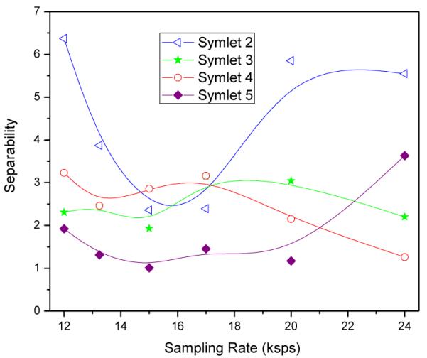
The sorting performance in terms of spike class separability between the different neuronal clusters in the feature space was also investigated over different sampling rates and Symlet bases functions. The class separability in this case is defined as the Euclidean distance between spike waveforms of two neurons represented in the compression domain by a fixed number of coefficients at a constant compression rate [30]. In Figure 13, quantification by the degree of separability is shown for different Symlets at different sampling rates. Clearly, Symlet 2 could support higher separability for most sampling frequencies and hence is the best choice for the sorting mode. Figure 14 shows the corresponding relation between spike class separability and compression rate.
Figure 13.
Relation between spike class separability and sampling rate for different Symlet bases functions
Figure14.

Spike class separability vs. compression rate
The implementations of Symlets 2 to 4 are well within the resource capability of the AGLN 250 nano-FPGA. The corresponding measured power consumptions are plotted in Figure 15. Overall, this kind of power-Symlet performance tradeoff is beneficial for different scenarios, operational modes and the system sampling rate.
Figure 15.

Power consumptions as a function of sampling rate and Symlet wavelet order.
Table III briefly summarizes a system level comparison of the features in the proposed neuroprocessor relative to some other state-of-the-art systems. From this Table, multiple systems that feature “record all, transmit all” strategies are reported. Many of these systems, however, are head-mounted and not fully implantable. Those that are implantable feature information extraction early in the data stream to cope with bandwidth limitations, but are limited by the number of channels that they could process at a given time [9]. Our system, on the other hand, circumvents all these limitations by featuring full implantability while preserving all the critical information in the multichannel recordings, which is the first report of such capability to the best of our knowledge.
Table III.
System Level Feature Comparison
In the closed-loop wireless telemetry system, power transfer takes place across the primary and secondary coils. The information about the power level is added to the neural data and sent back to the MIM utilizing load shift keying modulation (LSK) [36]. The forward telemetry from MIM to NIN for commands is implemented using amplitude shift keying (ASK) modulation of the power carrier. Both data communication and power transmission utilize 13.56 MHz (one of the ISM bands). The industrial, scientific and medical (ISM) radio bands are reserved internationally for the use of radio frequency (RF) energy for industrial, scientific and medical purposes other than communications. Hence, we do not anticipate any legal or interference issues with the proposed system.
V. CONCLUSION
In this paper, we reported on a fully implantable, programmable and multimodal neuroprocessor design to exclusively process high bandwidth neural signals collected from high density microelectrode arrays implanted in the brain. We demonstrated that the neuroprocessor can be efficiently implemented on a 5mm×5mm nano-FPGA, and consumes 5.19 mW of power to process 32 channels of neural data sampled at 25 ksps and 8-bit of resolution. This design brings the power density to 20.76 mW/cm2, which is well within the power density limits for clinical grade implants, estimated to be ~62 mW/cm2 [39, 40]. This is equivalent to a power/size demand to be less than 4.1 mW·mm2/channel, confirming its scalability feature. The system is programmable to cope with highly nonstationary neural signals over long-term chronic use. The system is also cost effective in making it well suited for basic neuroscience research as well as clinical BMI applications.
Acknowledgments
This work was supported by the National Institutes of Health under Grant NS062031.
Contributor Information
Fei Zhang, Department of Electrical and Computer Engineering, Michigan State University, East Lansing, MI 48824 USA (feizhang@msu.edu, aghagolz@msu.edu).
Mehdi Aghagolzadeh, Department of Electrical and Computer Engineering, Michigan State University, East Lansing, MI 48824 USA (feizhang@msu.edu, aghagolz@msu.edu).
Karim Oweiss, Department of Electrical and Computer Engineering and Neuroscience Program, Michigan State University, East Lansing, MI 48824 USA (koweiss@msu.edu).
References
- [1].Serruya MD, Hatsopoulos NG, Paninski L, Fellows MR, Donoghue JP. Brain-machine interface: Instant neural control of a movement signal. Nature. 2002;416:141–142. doi: 10.1038/416141a. [DOI] [PubMed] [Google Scholar]
- [2].Taylor DM, Helms Tillery SI, Schwartz AB. Direct cortical control of 3D neuroprosthetic devices. Science. 2002;296:1829–1832. doi: 10.1126/science.1070291. [DOI] [PubMed] [Google Scholar]
- [3].Oweiss KG, Mason A, Suhail Y, Kamboh AM, Thomson KE. A scalable wavelet transform VLSI architecture for real-time signal processing in high-density intra-cortical implants. IEEE Transactions on Circuits and Systems I: Regular Papers. 2007;54:1266–1278. [Google Scholar]
- [4].Asgarian F, Zhang F, Aghagolzadeh M, Kiani M, Ghovanloo M, Oweiss KG. iWIMNIS-A: A fully implantable Wireless Intracortical Multichannel Neural Interface System for neural recording in freely behaving subjects. in preparation. [Google Scholar]
- [5].Rizk M, Obeid I, Callender SH, Wolf PD. A single-chip signal processing and telemetry engine for an implantable 96-channel neural data acquisition system. Journal of Neural Engineering. 2007;4:309. doi: 10.1088/1741-2560/4/3/016. [DOI] [PubMed] [Google Scholar]
- [6].Harrison RR, Watkins PT, Kier RJ, Lovejoy RO, Black DJ, Greger B, Solzbacher F. A low-power integrated circuit for a wireless 100-electrode neural recording system. IEEE Journal of Solid-State Circuits. 2007;42:123–133. [Google Scholar]
- [7].Perelman Y, Ginosar R. An integrated system for multichannel neuronal recording with spike/LFP separation, integrated A/D conversion and threshold detection. IEEE Transactions on Biomedical Engineering. 2007;54:130–137. doi: 10.1109/TBME.2006.883732. [DOI] [PubMed] [Google Scholar]
- [8].Obeid I. Ph.D Thesis. Duke University; Durham, NC: 2004. A wireless multichannel neural recording platform for real time brain machine interface. [Google Scholar]
- [9].Moo Sung C, Zhi Y, Yuce MR, Linh H, Liu W. A 128-channel 6 mW wireless neural recording IC with spike feature extraction and UWB transmitter. IEEE Transactions on Neural Systems and Rehabilitation Engineering. 2009;17:312–321. doi: 10.1109/TNSRE.2009.2021607. [DOI] [PubMed] [Google Scholar]
- [10].Lee SB, Lee MH, Kiani M, Uei-Ming J, Ghovanloo M. An inductively powered scalable 32-channel wireless neural recording system-on-a-chip for neuroscience applications. IEEE Transactions on Biomedical Circuits and Systems. 2010;4:360–371. doi: 10.1109/TBCAS.2010.2078814. [DOI] [PMC free article] [PubMed] [Google Scholar]
- [11].Miranda H, Gilja V, Chestek CA, Shenoy KV, Meng TH. HermesD: A high-rate long-range wireless transmission system for simultaneous multichannel neural recording applications. IEEE Transactions on Biomedical Circuits and Systems. 2010;4:181–191. doi: 10.1109/TBCAS.2010.2044573. [DOI] [PubMed] [Google Scholar]
- [12].Yeager DJ, Holleman J, Prasad R, Smith JR, Otis BP. NeuralWISP: A wirelessly powered neural interface with 1-m range. IEEE Transactions on Biomedical Circuits and Systems. 2009;3:379–387. doi: 10.1109/TBCAS.2009.2031628. [DOI] [PubMed] [Google Scholar]
- [13].Song YK, Borton DA, Park S, Patterson WR, Bull CW, Laiwalla F, Mislow J, Simeral JD, Donoghue JP, Nurmikko AV. Active microelectronic neurosensor arrays for implantable brain communication interfaces. IEEE Transactions on Neural Systems and Rehabilitation Engineering. 2009;17:339–345. doi: 10.1109/TNSRE.2009.2024310. [DOI] [PMC free article] [PubMed] [Google Scholar]
- [14].Sodagar AM, Wise KD, Najafi K. A wireless implantable microsystem for multichannel neural recording. IEEE Transactions on Microwave Theory and Techniques. 2009;57:2565–2573. [Google Scholar]
- [15].Sodagar AM, Perlin GE, Ying Y, Najafi K, Wise KD. An implantable 64-channel wireless microsystem for single-unit neural recording. IEEE Journal of Solid-State Circuits. 2009;44:2591–2604. [Google Scholar]
- [16].Ming Y, Ghovanloo M. A flexible clockless 32-ch simultaneous wireless neural recording system with adjustable resolution; IEEE International Solid-State Circuits Conference; 2009.pp. 432–433. [Google Scholar]
- [17].Harrison RR, Kier RJ, Chestek CA, Gilja V, Nuyujukian P, Ryu S, Greger B, Solzbacher F, Shenoy KV. Wireless neural recording with single low-power integrated circuit. IEEE Transactions on Neural Systems and Rehabilitation Engineering. 2009;17:322–329. doi: 10.1109/TNSRE.2009.2023298. [DOI] [PMC free article] [PubMed] [Google Scholar]
- [18].Gosselin B, Sawan M. An ultra low-power CMOS automatic action potential detector. IEEE Transactions on Neural Systems and Rehabilitation Engineering. 2009;17:346–353. doi: 10.1109/TNSRE.2009.2018103. [DOI] [PubMed] [Google Scholar]
- [19].Chestek CA, Gilja V, Nuyujukian P, Kier RJ, Solzbacher F, Ryu SI, Harrison RR, Shenoy KV. HermesC: low-power wireless neural recording system for freely moving primates. IEEE Transactions on Neural Systems and Rehabilitation Engineering. 2009;17:330–338. doi: 10.1109/TNSRE.2009.2023293. [DOI] [PubMed] [Google Scholar]
- [20].Harris JG, Principe JC, Sanchez JC, Du C, She C. Pulse-based signal compression for implanted neural recording systems; IEEE International Symposium on Circuits and Systems, ISCAS 2008; 2008.pp. 344–347. [Google Scholar]
- [21].Sodagar AM, Wise KD, Najafi K. A fully integrated mixed-signal neural processor for implantable multichannel cortical recording. IEEE Transactions on Biomedical Engineering. 2007;54:1075–1088. doi: 10.1109/TBME.2007.894986. [DOI] [PubMed] [Google Scholar]
- [22].Santhanam G, Linderman MD, Gilja V, Afshar A, Ryu SI, Meng T, Shenoy K. HermesB: A continuous neural recording system for freely behaving primates. IEEE Transactions on Biomedical Engineering. 2007;54:2037–2050. doi: 10.1109/TBME.2007.895753. [DOI] [PubMed] [Google Scholar]
- [23].Gosselin B, Ayoub AE, Sawan M. A mixed-signal multi-chip neural recording interface with bandwidth reduction; IEEE Biomedical Circuits and Systems Conference; 2007; pp. 49–52. [DOI] [PubMed] [Google Scholar]
- [24].Song YK, Patterson WR, Bull CW, Beals J, Hwang N, Deangelis AP, Lay C, McKay JL, Nurmikko AV, Fellows MR, Simeral JD, Donoghue JP, Connors BW. Development of a chipscale integrated microelectrode/microelectronic device for brain implantable neuroengineering applications. IEEE Transactions on Neural Systems and Rehabilitation Engineering. 2005;13:220–226. doi: 10.1109/TNSRE.2005.848337. [DOI] [PubMed] [Google Scholar]
- [25].Liu W, Sivaprakasam M, Wang G, Zhou M, Granacki J, Lacoss J, Wills J. Implantable biomimetic microelectronic systems design. IEEE Engineering in Medicine and Biology Magazine. 2005;24:66–74. doi: 10.1109/memb.2005.1511502. [DOI] [PubMed] [Google Scholar]
- [26].Olsson R, Wise K. A three-dimensional neural recording microsystem with implantable data compression circuitry; 2005 IEEE International Solid-State Circuits Conference; 2005.pp. 558–559. [Google Scholar]
- [27].Mohseni P, Najafi K, Eliades SJ, Wang X. Wireless multichannel biopotential recording using an integrated FM telemetry circuit. IEEE Transactions on Neural Systems and Rehabilitation Engineering. 2005;13:263–271. doi: 10.1109/TNSRE.2005.853625. [DOI] [PubMed] [Google Scholar]
- [28].Patterson WR, Yoon-Kyu S, Bull CW, Ozden I, Deangellis AP, Lay C, McKay JL, Nurmikko AV, Donoghue JD, Connors BW. A microelectrode/microelectronic hybrid device for brain implantable neuroprosthesis applications. IEEE Transactions on Biomedical Engineering. 2004;51:1845–1853. doi: 10.1109/TBME.2004.831521. [DOI] [PubMed] [Google Scholar]
- [29].Hochberg LR, Serruya MD, Friehs GM, Mukand JA, Saleh M, Caplan AH, Branner A, Chen D, Penn RD, Donoghue JP. Neuronal ensemble control of prosthetic devices by a human with tetraplegia. Nature. 2006;442:164–171. doi: 10.1038/nature04970. [DOI] [PubMed] [Google Scholar]
- [30].Aghagolzadeh M, Oweiss K. Compressed and distributed sensing of neuronal activity for real time spike train decoding. IEEE Transactions on Neural Systems and Rehabilitation Engineering. 2009;17:116–127. doi: 10.1109/TNSRE.2009.2012711. [DOI] [PMC free article] [PubMed] [Google Scholar]
- [31].Oweiss KG. Statistical Signal Processing for Neuroscience and Neurotechnology. Academic Press; Elsevier: 2010. pp. 15–74. [Google Scholar]
- [32].Kamboh AM, Raetz M, Oweiss KG, Mason A. Area-power efficient VLSI implementation of multichannel DWT for data compression in implantable neuroprosthetics. IEEE Transactions on Biomedical Circuits and Systems. 2007;1:128–135. doi: 10.1109/TBCAS.2007.907557. [DOI] [PubMed] [Google Scholar]
- [33].Zhang F, Aghagolzadeh M, Oweiss K. An implantable neuroprocessor for multichannel compressive neural recording and on-the-fly spike sorting with wireless telemetry; Biomedical Circuits and Systems Conference (BioCAS), 2010 IEEE; 2010.pp. 1–4. [Google Scholar]
- [34].Zhang F, Aghagolzadeh M, Oweiss Karim. A low-power implantable neuroprocessor on nano-FPGA for brain machine interface applications; the 36th IEEE International Conference on Acoustics, Speech and Signal Processing; 2011. [Google Scholar]
- [35].Kiani M, Ghovanloo M. An RFID-based closed-loop wireless power transmission system for biomedical applications. IEEE Transactions on Circuits and Systems II: Express Briefs. 2010;57:260–264. doi: 10.1109/TCSII.2010.2043470. [DOI] [PMC free article] [PubMed] [Google Scholar]
- [36].Kiani M, Kwon KY, Zhang F, Oweiss K, Ghovanloo M. Evaluation of a closed loop inductive power transmission system on an awake behaving animal subject; the 33rd Annual International Conference of the IEEE Engineering in Medicine and Biology Society; 2011; [DOI] [PMC free article] [PubMed] [Google Scholar]
- [37]. http://www.actel.com/documents/IGLOO_nano_DS.pdf.
- [38].Oweiss KG. Ph.D Thesis. University of Michigan; Ann Arbor, MI: 2002. Multiresolution analysis of multichannel neural recordings in the context of signal detection, estimation, classification and noise suppression. [Google Scholar]
- [39].Sun Y, Huang S, Oresko JJ, Cheng AC. Programmable Neural Processing on a Smartdust for Brain-Computer Interfaces. IEEE Transactions on Biomedical Circuits and Systems. 2010;4:265–273. doi: 10.1109/TBCAS.2010.2049743. [DOI] [PubMed] [Google Scholar]
- [40].Zhang F, Aghagolzadeh M, Oweiss K. A Programmable and Implantable Microsystem for Multimodal Processing of Ensemble Neural Recordings; the 33rd Annual International Conference of the IEEE Engineering in Medicine and Biology Society; 2011; [DOI] [PubMed] [Google Scholar]