Abstract
Here, we report the fabrication of a graphene-based Bragg grating (one-dimensional photonic crystal) and experimentally demonstrate the excitation of surface electromagnetic waves in the periodic structure using prism coupling technique. Surface electromagnetic waves are non-radiative electromagnetic modes that appear on the surface of semi-infinite 1D photonic crystal. In order to fabricate the graphene-based Bragg grating, alternating layers of high (graphene) and low (PMMA) refractive index materials have been used. The reflectivity plot shows a deepest, narrow dip after total internal reflection angle corresponds to the surface electromagnetic mode propagating at the Bragg grating/air boundary. The proposed graphene based Bragg grating can find a variety of potential surface electromagnetic wave applications such as sensors, fluorescence emission enhancement, modulators, etc.
In the past few years, surface electromagnetic waves (SEWs) supported by semi-infinite one dimensional (1D) photonic crystals (PC) have been recognized and extensively studied for many applications such as sensors, fluorescence emission enhancement, enhancement of the Goos–Hänchen effect1,2,3,4,5,6,7,8,9,10,11,12. SEWs are non-radiative electromagnetic modes that appear on the surface of semi-infinite 1D photonic crystal (Bragg grating) and propagate along the PC/air interface with exponentially decaying (evanescent) field in each bounding medium. These modes are considered to be an alternative to surface plasmon polaritons which exists in a homogeneous semi infinite metal film. The major advantages of SEWs in comparison to surface plasmons are: (i) capability to tune the SEW excitation in a broad wavelength interval ranging from IR to near-UV, by selecting the appropriate dielectric materials and suitable design of PC structure and (ii) capability of strong coupling between SEW and incoming light due to the low loss in PC, which consist of dielectric materials3,5. The low loss in PC may provide higher intensity of SEW, which leads to much sharper resonance dips and high surface electromagnetic fields. In order to study the SEW excitation at optical frequencies, till date, high refractive index dielectric materials such as Si, TiO2, silicon nitride, etc have been used for the fabrication of 1D photonic crystals3,5,8. Here, we propose to employ graphene as an alternate high refractive index material for 1D Bragg grating fabrication, because of the unusual properties of graphene and its ability to absorb biomolecules more strongly for biosensing applications.
Graphene is a single two-dimensional plane of carbon atoms forming a hexagonal lattice13. Since graphene is a zero band gap semiconductor, the electronic properties of graphene have attracted much attention in both experimental and theoretical research14,15,16. Graphene based ultra high speed electronics devices such as field-effect transistors, pn-junctions diodes, terahertz devices, etc have been already proposed and demonstrated17,18,19. Apart from the electronic properties of graphene, the study of optical properties of graphene is also equally important for many technological applications due to its strong interaction with light in a broad wavelength interval. It is reported that the graphene exhibits universal optical conductivity from visible to infrared frequencies due to interband transition, leading to 2.3% light absorption in the case of monolayer graphene20. Since then graphene has been attracted a great deal of attention for photonics and optoelectronics applications such as optical modulators, photovoltaic devices, light emitting devices, photodetectors, saturable absorbers and ultrafast lasers, etc21,22,23,24,25,26,27. Recently, tremendous interest has been generated in the field of graphene plasmonics. The reported works on graphene plasmonics suggests that plasmons in graphene offer potential capabilities for future technological applications28,29,30. However, the losses in plasmon modes must be evaluated and minimized (by doping) prior to its usage graphene as a potential alternate low loss plasmonic material. Graphene plasmonics at terahertz and infrared frequencies have been experimentally demonstrated by many groups31,32,33. However, it is barely visible and very difficult to realize at optical frequencies. The photonic crystal waveguide analogy of graphene nanoribbons have been theoretically investigated by Benisty34. More recently, graphene based 1D and 2D photonic crystal at terahertz frequencies have been theoretically proposed by Berman et al35,36. Furthermore, the fabrication of tunable infrared plasmonic devices are proposed using graphene/insulator stacks (photonic crystal like structure)33. It shows that graphene based photonic crystals are promising for a variety of future applications. In this context, here we propose a graphene based Bragg grating (1D photonic crystal) and demonstrate the excitation of surface electromagnetic waves in the multilayer at optical frequencies using prism coupling technique. This is the first experimental demonstration of a graphene-based 1D photonic crystal, as well as the excitation of surface electromagnetic waves in the periodic structure. Interestingly, this phenomenon can be considered as an alternative to graphene plasmonics at optical frequencies.
Results
Design and fabrication of Bragg grating
In order to fabricate the graphene-based Bragg grating, alternating layers of high and low refractive index materials have been used. Transparent materials such as single layer graphene (SLG) and Poly methyl methacrylate (PMMA) have been used as the high and low refractive index materials, respectively. Since graphene opacity is a universal constant at optical frequencies (independent of wavelength), we assume that the graphene is a dielectric material with isotropic refractive index and light polarization does not affect on graphene refractive index. The refractive index of graphene at visible wavelength range is obtained using the Fresnel coefficients calculation,  , where C1 = 5.446 µm−1, is a constant and λ0 is the vacuum wavelength37,38. According to Bruna et al37, the above refractive index value can be used to describe the optical behavior of graphene (2D) to the bulk limit (graphite). The refractive index of graphene (n1) and PMMA (n2) at 633 nm wavelength is 3+i 1.149 and 1.49, respectively. The Bragg wavelength, the wavelength of maximum reflectance can be calculated from the expression,
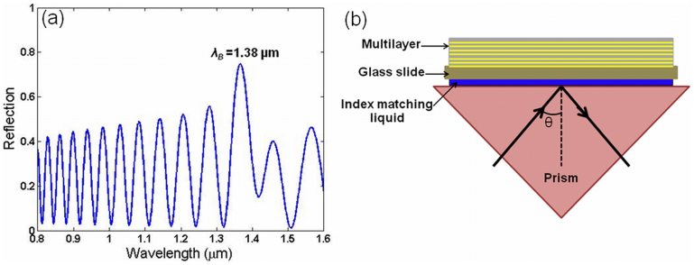
  , where d1 and d2 are the thicknesses of graphene and PMMA, respectively. In order to save the computation time and storage space (especially for FDTD simulation), the thickness of graphene (SLG) is assumed to be an unphysical value of 1 nm and PMMA thickness is taken as 470 nm. Note that the theoretically calculated Bragg wavelength is 1.4 µm. The Bragg wavelength is then numerically estimated by solving the 1D Helmholtz equations. The simulated reflection spectrum is shown in Fig. 1 (a) and estimated Bragg wavelength is around 1.38 µm. However, there is a slight discrepancy between theoretical and simulation results due to computational error. In addition, the reflection spectrum has been simulated using a graphene thickness of 0.5 nm and 0.34 nm (physical value). It is observed that the Bragg wavelength does not change when the graphene thickness is varied from 0.34 nm to 1 nm (see Supplementary Fig. S1). Fig. 1(b) represents the schematic diagram of sample configuration. A right angle prism of refractive index 1.515 (BK7 glass) is placed on the top of a glass slide (BK7) in which the graphene-based Bragg grating is attached and an index matching fluid is introduced between the prism and glass slide to provide the optical contact between them.
Figure 1. (a) Reflection spectrum of graphene-based Bragg grating calculated by solving the 1D Helmholtz equations and (b) Schematic diagram of Kretschmann configuration (prism coupling technique) for exciting the surface electromagnetic waves in the multilayer.
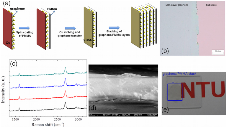
Schematic diagram of fabrication method is shown in Fig. 2 (a). The synthesis of large area, high quality monolayer graphene is possible using CVD method39. We used CVD for large area monolayer graphene preparation and monolayer of graphene is identified with an optical microscope (Fig. 2(b)) and subsequently confirmed by Raman spectroscopy (Fig. 2(c)). Figure 2(b) shows the as prepared monolayer graphene on a SiO2/Si substrate. The PMMA of thickness around 470 nm is spin coated on the graphene sample. The SEM cross sectional image of PMMA of average thickness 470 nm is shown in Fig. 2(d). The Bragg grating is realized by stacking of many graphene/PMMA layers on the glass slide (BK7). A large area Bragg grating (1D) with 8 bilayers of graphene/PMMA stack is realized and photograph of as prepared sample is shown in Fig. 2(e). In order to check the homogeneity of the graphene coverage, an indirect approach is employed by measuring the Raman spectrum of graphene from the different positions of the fabricated sample. Raman spectra have been collected from four regions on the sample by a Renishaw Raman system with a 2400 lines/mm grating and 532 nm laser (Fig. 2(c)). The clear G and G′ peaks from monolayer graphene layers in the sample were observed at ~1590 cm−1 and 2685 cm−1, which are from two in-plane optical phonons related to the first-order Raman scattering and the two-phonon double resonance process in graphene, respectively40. These Raman features are similar to those of a monolayer graphene in the previous studies41. Since same spin coating condition is used for fabricating the PMMA layers, we assume that the PMMA layers are almost homogeneous in the sample.
Figure 2. (a) Schematic diagram of fabrication procedure for graphene-based Bragg grating, (b) Optical image of CVD-grown monolayer graphene on the substrate (SiO2/Si), (c) Raman spectra of monolayer graphene at four different position of the fabricated structure, (d) SEM cross section image of PMMA with an average thickness of 470 nm, and (e) Photograph of as prepared stack with 8 bilayers (graphene/PMMA).
Experimental details
According to the theory, SEWs should exist at the interface of each of the two media (Bragg grating and air)42. However, in order to excite SEWs, the incoming beam has to match its momentum to that of the SEWs. It can be possible by passing the incident light through a prism to increase the wavevector component and hence to achieve the resonance at a given wavelength. This is similar to the phase matching condition used in the surface plasmon excitation. Hence a custom-built angular surface plasmon resonance (SPR) spectroscopy set-up is employed for the experimental investigation. Here, we used a 4-mW 632.8-nm He–Ne laser as our optical source to excite the surface electromagnetic waves in the structure. The polarization of the incident light is set as TM polarization and beam spot size is 1 mm in diameter. The configuration is based on the well-known Kretschmann configuration (prism coupling technique), which includes a right-angle prism coupler made from BK7 glass (Edmund Optics) with 40 mm length of legs and is immobilized on a rotary translation stage. The thin film with graphene/PMMA stacks is attached to the hypotenuse face of the prism with the aid of optical matching oil (Cargille Labs). The incident light passed through the right-angle face of the prism to the thin film of graphene/PMMA stack then reflected out. The intensity of the total internal reflected light changing with the incident angle is collected and monitored through a high-precision optical power meter (Newport 2832C). During the experiment, we focused the beam on the homogeneous part of the sample in order to get the exact reflectance for each incident angle.
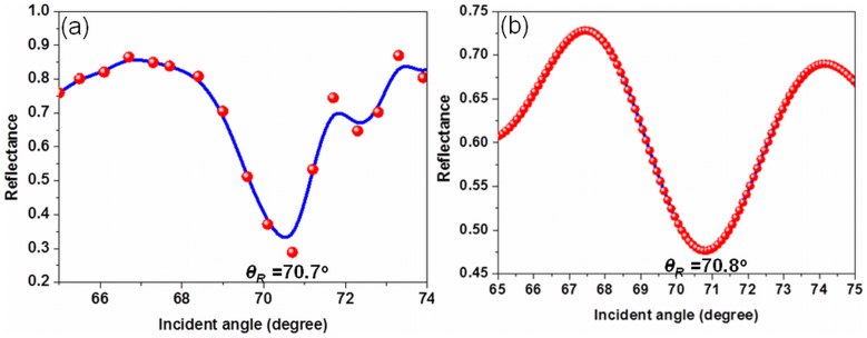
Figure 3(a) shows the experimental reflectance data obtained using prism coupling technique. Note that the reflectance system is calibrated against a highly reflective surface. The excitation of surface electromagnetic wave is recognized as the angle at which reflected intensity occurred is minimum (ATR minimum) and this ATR minimum angle has been taken as the resonance angle. From the figure, it is evident that the obtained resonance angle is 70.7°, which is greater than the angle of TIR (41.3°) between prism and air. Hence this deepest dip at resonance angle corresponds to the non-radiative SEW propagating at the Bragg grating/air boundary. In order to confirm the experimental data, reflectance diagram is simulated by solving the Fresnel's equations for multilayer structure. The simulated result is shown in Fig. 3 (b) and observed resonance angle is 70.8°. It is found to correlate well with the experimentally observed value of 70.7°. In order to check the influence of graphene thickness on resonance angle, the reflectance diagram is further simulated using a thickness of 0.5 nm and 0.34 nm (physical value) and observed that there is no change in resonance angle when the graphene thickness is varied from 0.34 nm to 1 nm (see Supplementary Fig. S2). It is also found that the resonance angle decreases when the excitation wavelength increases (see Supplementary Fig. S3).
Figure 3.
(a) Experimental reflectance diagram (as a function of incident angle) acquired using prism coupling technique at optical frequency, where the blue line is for eye guide.The observed resonance angle is 70.7° and (b) Simulated reflectance date by solving the Fresnel's equations for multilayer structure, estimated resonance angle is 70.8°.
Surface dispersion diagram
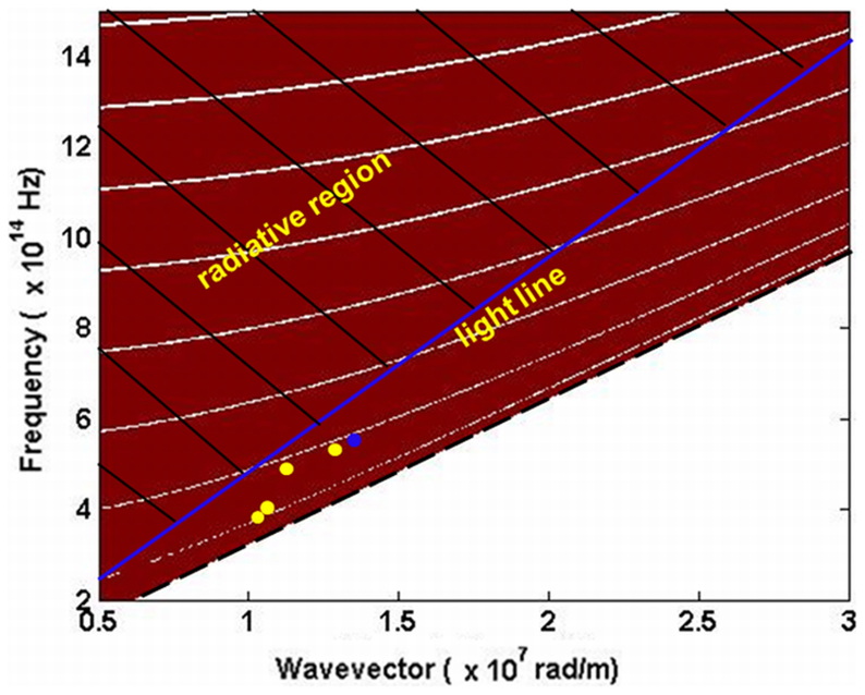
Figure 4 shows the dispersion diagram (band structure) of frequency versus wave vector projected in to the plane of the interface of the structure for TM polarized waves. Transfer Matrix method43 has been used to determine the band structure of the proposed structure. It is important to plot such diagram to relate the experimental surface wave dispersion results to photonic band gap of the Bragg grating1. In Fig. 4, narrow white regions represent the photonic bands (non-radiative regions) within the Bragg grating. The obtained photonic bands are narrow due to the smaller thickness of graphene. It is also evident from the figure that at certain frequencies and wave vectors, the photonic bands shirk to zero. However, such behavior is not observed in the case of TE polarized waves (see Supplementary Fig. S4). It is already reported that when the incident angle equal to the Brewster angle, the photonic bands shrink to zero for TM polarized waves43. At any given frequency, incident light can have wave vector values ranging from zero (normal incidence) to a maximum value of 2πf/c (light travelling tangentially parallel to the surface, ie θ = 90°). Therefore we plotted the light line for air using the maximum value (2πf/c) and indicated by blue solid line in the dispersion diagram. The area limited by this line (hatched region) corresponds to surface wave vector values that are radiative on the air side of the interface. The red dark region in the dispersion diagram indicates the radiative regions (allowed bands) within the Bragg grating. The surface electromagnetic waves exist in the non-radiative region (photonic bands) of the dispersion diagram and away from the air light line. It means that SEWs cannot radiate either into the air side or into the Bragg grating. The parallel wave vector of the mode at 633 nm excitation wavelength, calculated using the expression 2π(f/c)n sinθ is 1.42 X 10⁷ rad/m, where n is the refractive index of prism. This value is indicated by blue dot in the dispersion diagram. It is visible from the figure that this value appear away from the air light line and occur close to second band edge, but within the non-radiative region of the dispersion diagram. The attenuation of the Bragg grating material is relatively weak at the band edges (close to the band edges) so that the light is able to tunnel through the multilayer and to excite the SEW3. There is no physical meaning beyond the dotted dark line. It shows that the experimental results are qualitative agreement with the theoretical dispersion diagram.
Figure 4. Surface dispersion diagram (band structure) of graphene-based Bragg grating for TM polarization.
Radiative and non-radiative regions (photonic bands) are represented by red dark region and narrow white regions, respectively. Light line for air is indicated by solid (blue) line. The hatched region represents the surface wave vector values that are radiative on the air side of the interface. Yellow dots represent the numerically estimated wave vector values for wavelengths 800 nm, 750 nm, 700 nm and 650 nm, and blue dot represents the experimentally obtained wave vector value for the wavelength 633 nm.
Further, the resonance angles are numerically calculated for four different excitation wavelengths (see Supplementary Fig. S3) and located their wave vector values in the dispersion diagram (yellow dots). All the wave vector values are well beyond the air light line and close to one of the photonic band edges, but within the non-radiative region. It is also possible to move the surface mode dispersion through the photonic bands from one edge to the other when the termination layer of the Bragg grating is varied42.
Surface mode electromagnetic field distribution
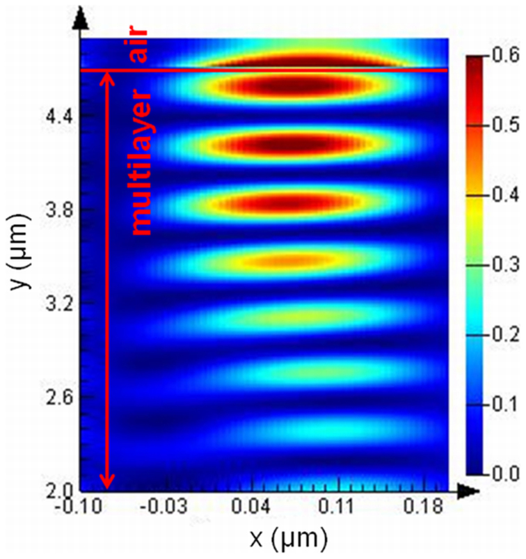
The surface mode electromagnetic field distribution is simulated using finite difference time domain (FDTD) method. The smallest spatial grid size (0.1 nm) is used for the iteration to maintain the accuracy and stability of FDTD calculations. The electromagnetic field profile is simulated by assuming that the light is incident at a resonant coupling angle of 70.7° through the prism. Figure 5 illustrates the electric field distribution as a function of depth along the multilayer. Here, the output electric field is normalized with respect to the incident excitation field. The intensity is decaying along the y-direction of the multilayer and field oscillates many times throughout the multilayer. It is evident from the figure that the electromagnetic field enhancement occurs within the last layer of Bragg grating when the surface mode is excited. That means the mode at the band edge has less attenuation and thus the evanescent filed can penetrate much further into Bragg grating, which itself prove the excitation of SEW in the proposed configuration. Maximum field enhancement factor is observed at Bragg grating/air interface and this enhancement factor is due to the tighter confinement of mode to the surface. This large field enhancement can be used for improving the sensitivity of sensors, fluorescence emission enhancement and enhancement of the Goos–Hänchen effect.
Figure 5. Simulated surface mode electromagnetic field distribution of graphene-based Bragg grating as a function of depth along the multilayer.
E-field is decaying along the y-direction of the multilayer.
Discussion
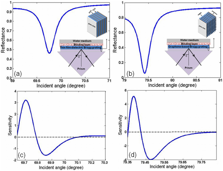
Here, we demonstrate the proof-of-principle functionality of the proposed graphene-based Bragg grating. In order to show the advantages of the proposed device, a biosensor configuration based on graphene-based Bragg grating and regular thin film dielectric Bragg grating is numerically proposed, as shown in Fig. 6 (inset). In both configurations, the Bragg grating is attached via index matching fluid on the top of the BK7 glass prism. We assume that the binding layer of thickness 100 nm consists of biomolecules of refractive index 1.46, prepared in water (e.g. ssDNA) and it covers the whole Bragg grating38,44. The thin film dielectric Bragg-grating (8 bilayers) consists of alternating layers of TiO2 and SiO2. The thickness of TiO2 and SiO2 are taken as 169 nm and 247 nm, respectively3. At 633 nm wavelength, the refractive index of dielectrics is directly taken from Shinn et al.5. While the graphene-based Bragg grating consists of an additional graphene termination layer. As mentioned above, the surface mode dispersion can be moved through the photonic bands when the termination layer of the Bragg grating has been varied.
Figure 6. Simulated reflectance diagram (a) for regular thin film dielectric Bragg grating, (b) for graphene-based Bragg grating terminated with an additional layer of graphene.
Corresponding sensitivity plot (c) for regular thin film dielectric Bragg grating, (d) for graphene-based Bragg grating terminated with an additional layer of graphene.
Figure 6 (a) and Fig. 6 (b) respectively represent the reflectance plot of thin film dielectric Bragg grating and graphene-based Bragg grating. The reflectance plots show a deepest, narrow dip for graphene-based Bragg grating as compared to regular thin film dielectric Bragg grating. It shows that the proposed structure has low loss and maximum SEW excitation compared to thin film dielectric Bragg grating.
Additionally, we calculated the sensitivity of both configurations by assuming that the refractive index (n) of binding layer change due to biomolecular reactions, however there is no change in the thickness of binding layer. The sensitivity can be defined as dR/dn, where R is the reflectance and n is the refractive index of biomolecules44. The sensitivity of biosensor based on thin film dielectric Bragg grating and proposed Bragg grating is shown in Fig. 6 (c) and Fig. 6(d), respectively. At the resonance angle, sensitivity values are almost zero, because the sensitivity corresponds to the slope in the reflectance curve. Also, the magnitude of the positive peak is greater than that of the negative peak, because the gradient in reflectance is steeper for the incidence angle approaching the resonance angle44. In the case of graphene-based Bragg grating, the maximum sensitivity is found to be 5.2, while the regular thin film dielectric Bragg grating has a maximum sensitivity of 3.2. It should be noted that the positive value of sensitivity is taken as the maximum sensitivity. It is shown that the sensitivity of the graphene-based Bragg grating is 1.6 times higher than that of thin film dielectric Bragg grating, implying that the proposed Bragg grating can be used as an effective way to achieve a high sensitivity. It is attributed to the fact that the ability of graphene to adsorb biomolecules more strongly, due to the π-stacking interactions between graphene's hexagonal cells and carbon-based ring structure in the biomolecules38,45. In addition, the proposed graphene/PMMA stack is more flexible compared to regular thin film dielectric Bragg gratings. Therefore, the excitation of SEWs in a graphene based Bragg grating using prism coupling technique can expected to find variety of potential surface electromagnetic wave applications.
In summary, the excitation of surface electromagnetic waves in a graphene-based Bragg grating has been experimentally investigated. At optical frequency, prism coupling technique was used to explore the excitation of SEW in the multilayer. The proposed graphene-based 1D periodic structure has low loss, which gives a narrow angular reflectivity resonance and high surface fields. The experimental results are also compared with theoretical dispersion diagram of Bragg grating. The large field enhancements associated with this structure could be a good replacement for thin film dielectric Bragg grating in many SEW applications such as sensors and modulators.
Methods
Graphene was grown on copper foil by using low-pressure CVD39. Before the surface-catalyzed growth, the copper substrate was annealed at 1000°C for 20 min where H2 was used to remove surface oxide layers with a flow rate of 10 sccm. After that, 40 sccm methane was introduced as a carbon source. Monolayer graphene on high-purity (99.999%) copper foil was obtained at 1000°C under a chamber pressure of 3.6 Torr. The PMMA (950 PMMA A resist from Microchem) was spin coated on graphene/copper foil at an rpm of 2500, in order to get a thickness of around 470 nm. Then the sample was transferred as described in a previous report46. The aqueous solution of iron nitride (FeNO3)3 was employed to etch copper foil and isolate graphene/PMMA layer. Later, the graphene film was transferred into deionized water to rinse for several times. Subsequently, BK7 glass substrate was used to lift up the first graphene/PMMA layer. This process is repeated until desirable layer numbers were achieved. 1D Bragg grating was fabricated by stacking of eight graphene/PMMA layers.
About custom-built angular surface plasmon resonance (SPR) spectroscopy set-up was clearly explained in the main text. A Raman spectroscopic system (CRM 200, WITec) with an excitation source of diode-pumped double-frequency Nd:YAG laser (532 nm) was used for recording of Raman spectra and hence confirming of monolayer graphene. The laser power was kept below 0.1 mW to avoid the heat-induced deformation of the sample.
Theoretical reflection spectrum and surface dispersion diagram of graphene-based Bragg grating was generated using Matlab code. Reflectivity diagram was also generated using Matlab code and checked the results using WINSPALL software. However, commercially available lumerical FDTD software was employed for surface mode electromagnetic field calculation.
Author Contributions
K. V. S. and J. S. fabricated the device. The experiments were conceived, designed and carried out by S. Z., K. V. S., K.-T. Y. and T. Y. All simulations were carried out by K. V. S. K. V. S. and S. Z. co-wrote the manuscript. T. Y. and K.-T. Y. provided suggestions, and all authors commented on the manuscript.
Supplementary Material
Supplementary information
Acknowledgments
The authors acknowledge the financial support received through National Research Foundation NRF RF Award No. NRF-RF2010-07 and MoE Tier 2 MoE2009-T2-037. K. V. S. thanks Mr. T. Borriboon (MAE, NTU) for support with Matlab simulations.
References
- Robertson W. M. & May M. S. Surface electromagnetic wave excitation on one-dimensional photonic band-gap arrays. Appl. Phys. Lett. 74, 1800–1802 (1999). [Google Scholar]
- Gaspar-Armenta J. A., Villa F. & Lopez-Rios T. Surface waves in finite one-dimensional photonic crystals: Mode coupling. Opt. Comm. 216, 379–384 (2003). [Google Scholar]
- Robertson W. M. Experimental measurement of the effect of termination on surface electromagnetic waves in one-dimensional photonic bandgap arrays. J. Lightwave Technol. 17, 2013–2017 (1999). [Google Scholar]
- Villa F. et al. Photonic crystal sensor based on surface waves for thin-film characterization. Opt. Lett. 27, 646–648 (2002). [DOI] [PubMed] [Google Scholar]
- Shinn M. & Robertson W. M. Surface plasmon-like sensor based on surface electromagnetic waves in a photonic band-gap material. Sensors and Actuators B 105, 360–364 (2005). [Google Scholar]
- Wang B. et al. Surface waves in photonic crystal slabs. Phys. Rev. B 74, 195104 (2006). [Google Scholar]
- Liscidini M. & Sipe J. E. Enhancement of diffraction for biosensing applications via Bloch surface waves. Appl. Phys. Lett. 91, 253125 (2007). [Google Scholar]
- Descrovi E. et al. Near-field imaging of Bloch surface waves on silicon nitride one-dimensional photonic crystals. Opt. Exp. 16, 5453–5464 (2008). [DOI] [PubMed] [Google Scholar]
- Vandenbem C. Electromagnetic surface waves of multilayer stacks: coupling between guided modes and Bloch modes. Opt. Lett. 33, 2260–2261 (2008). [DOI] [PubMed] [Google Scholar]
- Soboleva I. V., Descrovi E., Summonte C., Fedyanin A. A. &. Giorgis F. Fluorescence emission enhanced by surface electromagnetic waves on one-dimensional photonic crystals. Appl. Phys. Lett. 94, 231122 (2009). [Google Scholar]
- Ballarini M. et al. Bloch surface waves-controlled emission of organic dyes grafted on a one-dimensional photonic crystal. Appl. Phys. Lett. 99, 043302 (2011). [Google Scholar]
- Wan Y. et al. Nearly three orders of magnitude enhancement of Goos-Hanchen shift by exciting Bloch surface wave. Opt. Exp. 20, 8998–9003 (2012). [DOI] [PubMed] [Google Scholar]
- Novoselov K. S. et al. Electric field effect in atomically thin carbon films. Science 306, 666–669 (2004). [DOI] [PubMed] [Google Scholar]
- Novoselov K. S. et al. Two-dimensional gas of massless Dirac fermions in graphene. Nature 483, 197–200 (2005). [DOI] [PubMed] [Google Scholar]
- Zhang Y. B., Tan Y. W., Stormer H. L. &. Kim P. Experimental observation of the quantum Hall effect and Berry's phase in graphene. Nature 438, 201–204 (2005). [DOI] [PubMed] [Google Scholar]
- Cong C., Yu T., Saito R., Dresselhaus G. F. &. Dresselhaus M. S. Second-order overtone and combination Raman modes of graphene layers in the range of 1690–2150 cm(-1). ACS Nano 5, 1600–1605 (2011). [DOI] [PubMed] [Google Scholar]
- Liang G., Neophytou N., Nikonov D. E. & Lundstrom M. S. Performance projections for ballistic graphene nanoribbon field-effect transistors. IEEE Trans. Electron Devices 54, 677–682 (2007). [Google Scholar]
- Williams J. R., DiCarlo L. & Marcus C. M. Quantum Hall effect in a gate-controlled p-n junction of graphene. Science 317, 638–641 (2007). [DOI] [PubMed] [Google Scholar]
- Ryzhii V. Terahertz plasma waves in gated graphene heterostructure. Jpn. J. Appl. Phys. 45, L923–L925 (2006). [Google Scholar]
- Nair R. R. et al. Fine structure constant defines visual transparency of graphene. Science 320, 1308–1308 (2008). [DOI] [PubMed] [Google Scholar]
- Shang J., Yu T., Lin J. & Gurzadyan G. G. Ultrafast electron optical phonon scattering and quasiparticle lifetime in CVD-grown graphene. ACS Nano 5, 3278–3283 (2011). [DOI] [PubMed] [Google Scholar]
- Liu M. et al. A graphene-based broadband optical modulator. Nature 474, 64–67 (2011). [DOI] [PubMed] [Google Scholar]
- Bae S. et al. Roll-to-roll production of 30-inch graphene films for transparent electrodes. Nature Nanotech 4, 574–578 (2010). [DOI] [PubMed] [Google Scholar]
- Matyba P. et al. Graphene and mobile ions: The key to all-plastic, solution-processed light-emitting devices. ACS Nano 4, 637–642 (2010). [DOI] [PubMed] [Google Scholar]
- Xia F., Mueller T., Lin Y.-M., Valdes-Garcia A. & Avouris P. Ultrafast graphene photodetector. Nature Nanotech. 4, 839–843 (2009). [DOI] [PubMed] [Google Scholar]
- Bao Q. et al. Atomic layer graphene as a saturable absorber for ultrafast pulsed lasers. Adv. Funct. Mater. 19, 3077–3083 (2010). [Google Scholar]
- Song Y. W., Jang S. Y., Han W. S. & Bae M. K. Graphene mode-lockers for fiber lasers functioned with evanescent field interaction. Appl. Phys. Lett. 96, 051122 (2010). [Google Scholar]
- Jablan M., Buljan H. & Soljacic M. Plasmonics in graphene at infrared frequencies. Phys. Rev. B 80, 245435 (2009). [Google Scholar]
- Nikolaenko A. E. et al. Nonlinear graphene metamaterial. Appl. Phys. Lett. 100, 181109 (2012). [Google Scholar]
- Koppens F. H. L., Chang D. E. & Garcia de Abajo J. G. Graphene plasmonics: A platform for strong light-matter interaction. Nano Lett 11, 3370–3377 (2011). [DOI] [PubMed] [Google Scholar]
- Zhou W. et al. Atomically localized plasmon enhancement in monolayer graphene. Nature Nanotech 7, 161–165 (2012). [DOI] [PubMed] [Google Scholar]
- Ju L. et al. Graphene plasmonics for tunable terahertz metamaterials. Nature Nanotech 6, 630–634 (2011). [DOI] [PubMed] [Google Scholar]
- Yan H. et al. Tunable infrared plasmonic devices using graphene/insulator stacks. Nature Nanotech 7,330–334 (2012). [DOI] [PubMed] [Google Scholar]
- Benisty H. Graphene Nanoribbons: Photonic crystal waveguide analogy and minigap stripes. Phys. Rev. B 79, 155409 (2009). [Google Scholar]
- Berman O. L., Boyko V. S., Kezerashvili R. Y., Kolesnikov A. A. & Lozovik Y. E. Graphene-based photonic crystal. Phys. Lett. A 374, 4784–4786 (2010). [Google Scholar]
- Berman O. L. & Kezerashvili R. Y. Graphene-based one-dimensional photonic crystal. J. Phys: Condens. Matter 24, 015305 (2012). [DOI] [PubMed] [Google Scholar]
- Bruna M. & Borini S. Optical constants of graphene layers in the visible range. Appl. Phys. Lett. 94, 031901 (2009). [Google Scholar]
- Wu L., Chu H. S., Koh W. S. & Li E. P. Highly sensitive graphene biosensors based on surface plasmon resonance. Opt. Exp. 18, 14395–14400 (2010). [DOI] [PubMed] [Google Scholar]
- Li X. et al. Large-area synthesis of high-quality and uniform graphene films on copper foils. Science 324, 1312–1314 (2009). [DOI] [PubMed] [Google Scholar]
- Malard L. M. et al. Raman spectroscopy in graphene. Phys. Rep. 473, 51–87 (2009). [Google Scholar]
- Li X. et al. Evolution of graphene growth on Ni and Cu by carbon isotope labeling. Nano Lett. 9, 4268–4272 (2009). [DOI] [PubMed] [Google Scholar]
- Ramos-Mendieta F. & Halevi P. Propagation constant-limited surface modes in dielectric superlattices. Opt. Commun. 129, 1–5 (1996). [Google Scholar]
- Yeh P., Yariv A. & Hong C.-S. Electromagnetic Propagation in Periodic Stratified Media. I. General Theory. J. Opt. Soc. Am. 67, 423–438 (1977). [Google Scholar]
- Choi S. H. et al. Graphene on silver substrates for sensitive surface plasmon resonance imaging biosensors. Opt. Exp. 19, 458–466 (2011). [DOI] [PubMed] [Google Scholar]
- Tang Z. et al. Constraint of DNA on functionalized graphene improves its biostability and specificity. Small 6, 1205–1209 (2010). [DOI] [PubMed] [Google Scholar]
- Li X. et al. Transfer of Large-Area Graphene Films for High-Performance Transparent Conductive Electrodes. Nano Lett. 9, 4359–4363 (2009). [DOI] [PubMed] [Google Scholar]
Associated Data
This section collects any data citations, data availability statements, or supplementary materials included in this article.
Supplementary Materials
Supplementary information


