Abstract
Depth of Interaction (DOI) information can improve quality of reconstructed images acquired from Positron Emission Tomography (PET), especially in high resolution and compact scanners dedicated for breast, brain, or small animal imaging applications. Additionally, clinical scanners with time of flight capability can also benefit from DOI information. One of the most promising methods of determining DOI in a crystal involves reading the signal from two ends of a scintillation crystal, and calculating the signal ratio between the two detectors. This method is known to deliver a better DOI resolution with rough crystals compared to highly polished crystals. However, what is still not well studied is how much of a tradeoff is involved between spatial, energy, temporal, and DOI resolutions as a function of the crystal surface treatment and geometry with the use of Silicon Photomultipliers (SiPM) as the photo detectors. This study investigates the effects of different crystal surface finishes and geometries on energy, timing and DOI resolutions at different crystal depths. The results show that for LYSO scintillators of 1.5×1.5×20 mm3 and 2×2×20 mm3 with their surfaces finished from 0.5 to 30 micron roughness, almost the same energy and coincidence timing resolutions were maintained, around 15% and 2.4 ns respectively across different crystal depths, while the DOI resolutions were steadily improved from worse than 5 mm to better than 2 mm. They demonstrate that crystal roughness, with proper surface preparing, does not have a significant effect on the energy and coincidence timing resolutions in the crystals examined, and there does not appear to be a tradeoff between improving DOI resolution and degrading other detector performances. These results will be valuable to guide the selection of crystal surface conditions for developing a DOI measurable PET detector with a full array of LYSO scintillators coupled to SiPM arrays.
Keywords: Silicon Photomultiplier, Depth Of Interaction, Positron Emission Tomography, Gamma Ray Detector
1. Introduction
It is well known that parallax error is a limiting factor for high spatial resolution in small bore PET scanners, such as those dedicated to small animal, breast, or brain imaging. Many such current systems reduce parallax errors by reducing the length of the crystals at the cost of system sensitivity. Knowledge of the depth of interaction (DOI) of individual gamma interactions would allow a reduction in parallax error without shortening the scintillator length. Various methods of measuring DOI information have been proposed and investigated including a single-ended-scintillator readout using measurement of light spread, pho-switch detectors, and mapping various depth positions to different x–y positions in a 2D flood map [1–3]. Alternatively, a dual-ended-scintillator (DES) readout technique generally compares the amount of light collected at either end of the scintillator array, where the light differential is generated either by light loss at reflection boundaries using slightly absorptive reflectors, or by light scattering at reflection boundaries using diffuse reflectors, crystal micro-cracks, or rough surfaces [4–6]. Compared to single-ended-scintillator readout with complicated light sharing or multiple scintillator layer techniques, DES method has the advantages of reduced mechanical complexity and continuous DOI sampling at the cost of using two photon sensors.
In this work we investigate the ability of Silicon Photomultipliers (SiPM) to measure DOI using a diffuse reflector with a DES readout technique. While the basic techniques of DOI encoding have been under investigation for decades, newly available compact SiPM arrays are well suited to DES readout due to their high signal-to-noise ratio and small form factor to allow a reinvestigation of the existing methods. Additionally, the falling price of SiPM arrays has made the overall cost of a DSE readout based PET detector near parity with a single-ended-scintillator traditional PMT readout. One area of open investigation with DES readout technique is the effect of surface finish on the essential performance properties of the detector when read out with a SiPM. The critical performance properties of a DOI measurable PET detector are energy, timing and DOI resolutions, and the accuracy of crystal interaction identification. It is essential to balance these performances with a suitable crystal surface finish in order to have a detector with the best overall response. While the effect of surface treatment on DOI resolution has previously been investigated with the use of photomultiplier tubes (PMT) and Avalanche Photodiodes (APD) [4, 6, 7], SiPMs have a different noise characteristic than either PMTs or APDs, in that they have a low pedestal, but a high dark-count rate [8]. The effect of the noise intrinsic to SiPMs, particularly the dark-counts, may cause a different tradeoff of energy, timing, and DOI resolutions with surface treatment than observed in either PMT or APD measurement. Additionally, the previous studies were performed with chemical etching which has a limited reproducibility, since a finished surface depends not only the reproducible etching process but also the surface conditions at the beginning of the process, which will depend on the particular cutting techniques used, and should be expected to vary between vendors.
2. Materials and Methods
2.1 Scintillator and surface treatment
The crystals used in this experiment were LYSO scintillators with 1.5×1.5 and 2×2 mm2 in cross section. They were delivered with saw cut finishes from the manufacturer (Agile Technologies, Knoxville, TN, USA). The crystals with 20 mm length were used for studying the effect of crystal cross section and surface finish on detector performance. Each of the four axial sides along the crystal depth was mechanically finished with different smoothness from 5.0 to 30 micron using lapping films (Precision Surface International, Inc., Houston, TX), with an additional crystal polished to 0.5 micron finish by the manufacturer. In addition, the crystals with 20, 30 and 40 mm length and both 1.5×1.5 and 2×2 mm2 cross sections with saw cut surface finish were used for studying the effect of crystal length. This yielded total 16 different combinations of crystal geometries and surface finishes. Each individual LYSO scintillator was wrapped with multiple layers of white Teflon tape, which is predominately a Lambertian reflector although with some specular components increasing in significance at high angles of incidence, to minimize light loss from photon escape [9]. The two ends of each crystal were mirror polished by the manufacturer.
2.2 Photon Sensor
Two SiPM arrays (SPMArray2, SensL, Ireland) were used for this study. Each SiPM array is composed of 16 individual SiPM pixels, each with a 2.85×2.85 mm2 active area and a 3.2 mm pixel pitch. Each pixel is composed of 3640 individual microcells of 35 µm each. Each array has a 0.5 mm thick entrance glass window. The reported dark count rate is 8 MHz per pixel with nominal operation bias at 32V (3V above breakdown). The intrinsic signal peaking and relaxation times are around 40 and 160 ns, respectively. Only one single SiPM pixel from each SiPM array was used in this study for detecting photons from each end of a single LYSO scintillator.
2.3 Experimental Setup
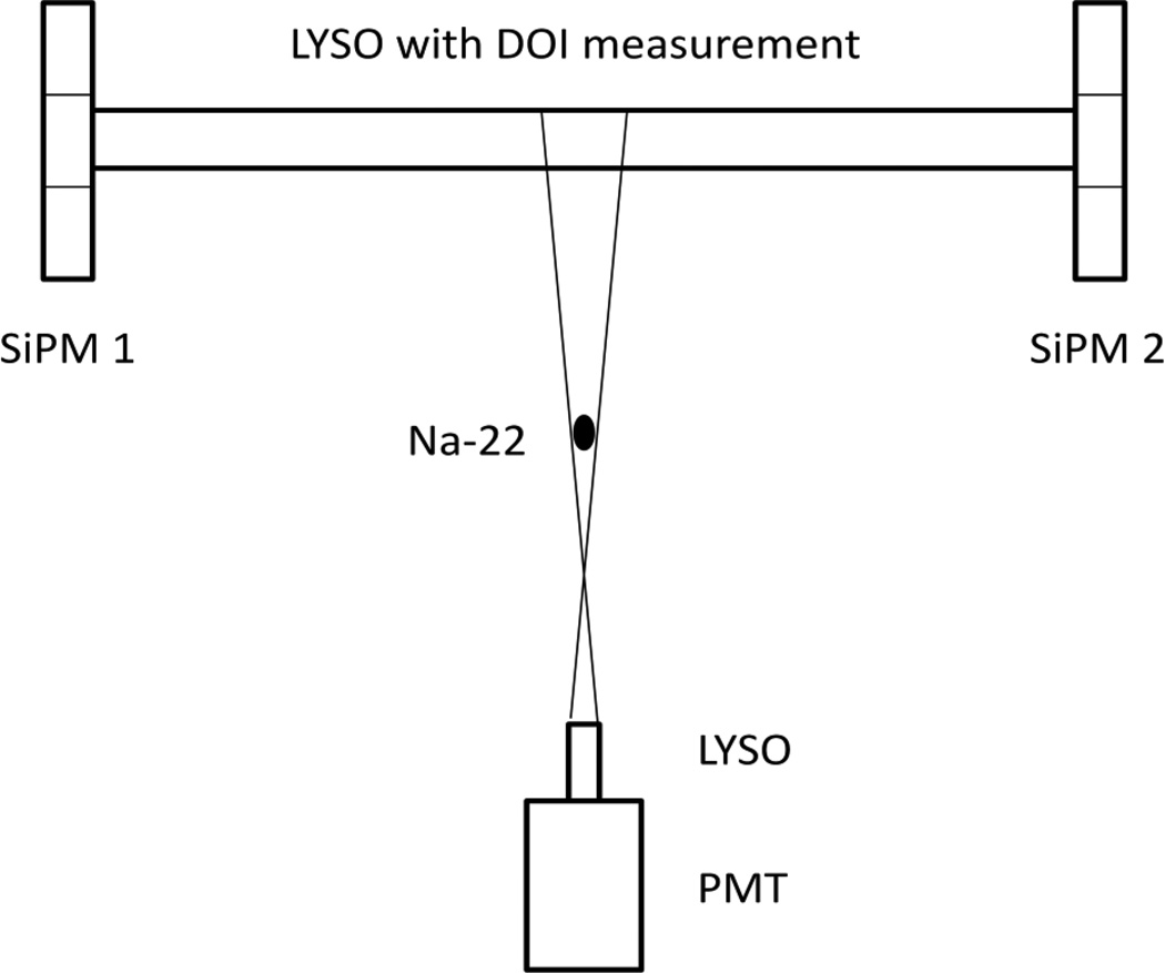
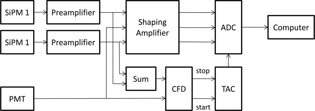
As shown in Fig. 1, two SiPM arrays were mechanically held in place and optically coupled to both ends of the LYSO with optical grease (BC-630, Saint Gobain, OH, USA). Single pixel readout was used to reduce noise and optimize energy, timing, and DOI resolutions. Annihilation 511 keV gamma rays from a Na-22 disk source with a 1.0 mm thickness and 5.0 mm radius but aligned along the 1.0 mm direction were electronically collimated to irradiate a narrow DOI region through coincidence events with an additional LYSO crystal of 1×0.7×10 mm3 optically coupled to a single channel PMT (R7400, Hammamatsu Corp. Japan). The signals from the two sides of the LYSO scintillator were passed through the manufacturer supplied pre-amp board using AD8132 amplifiers, then summed and fed into a constant fraction discriminator (CFD, Canberra model 454), with a minimum trigger threshold set above the electronic noise to trigger timing signals. A time-to-amplitude convertor (TAC, Canberra model 2145) was used to select coincident events within a 20 ns time window. The summed singles were amplified using a shaping amplifier (CAEN model N568LC) and digitized through a multi-channel amplitude-to-digital convertor (ADC, Datel model PCI-416). The signal amplitudes of individual SiPM, PMT and TAC for each coincident event were acquired with a LabView (National Instruments, TX, USA) based PC data acquisition (Fig. 2).
Fig. 1.
Schematic diagram of a dual-ended-scintillator readout and experiment setup for DOI measurements
Fig. 2.
Schematic diagram of data acquisition electronics for the timing, energy, and DOI measurements.
2.4 Measurement and Data Analysis
The overall measurement and data analysis were similar to what have been applied in the previous similar studies that used PMT or APD photon sensors [4, 6, 7]. Briefly, we measured the energy, coincidence timing and DOI resolutions at different DOI positions with the electronically collimated Na-22 source stepping over the entire depth of the crystal with 1.0 mm each step. We repeated these measurements for different crystal geometries and surface finishes.
In principle, the data analysis can be applied without the requirement of balanced amplification gains between the two SiPMs and their electronics. However, for characterizing detector performance, it is preferred to correct such gain difference so that the detector performance along the crystal depth can be calculated without any effect from imbalanced gains from detectors and data acquisitions. A software based gain balance factor, K, was calculated based on the measured signals,
| (1) |
where S1 and S2 are the signal amplitudes measured from the first and second SiPM detectors respectively, and the subscripts a and b indicate the DOI positions at two opposite crystal edges. This software gain correction factor K, which reflects the difference between the amplification gains if the light collections at both crystal ends are the same, was calculated for each crystal and multiplied to acquired signal S2.
The energy of a measured event equals to
| (2) |
The signal ratio is defined as
| (3) |
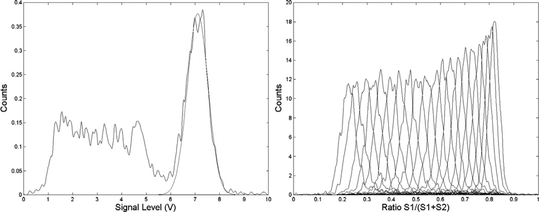
At any given depth the signal ratio R was calculated for the photopeak events with a 350 keV energy threshold. A typical measured energy spectrum and the histograms of signal ratio R at different DOI positions are shown in Fig. 3. The mean and full width at half maximum (FWHM) calculated from these histograms were used to determine the value and variation of signal ratio R as a function of DOI positions, and subsequently the DOI resolution which was calculated as the physical distance the collimated source must traverse in order to separate two neighboring R histograms at their FWHM [4, 10, 11].
Fig. 3.
Left: Energy spectrum from a 2×2×20 mm3 crystal with 30 µm finish, which is fitted with a Gaussian to the photopeak. The collimated beam for this dataset is aligned at the center of the 20 mm long crystal. Right: R space histograms for the same crystal. The source positions were 1 mm apart. The DOI response function is the centroid location of the R histogram as a function of source position, while the error is given as the FWHM of the R histogram for the same dataset.
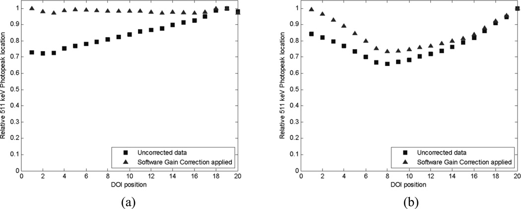
Typical distributions of energy at 511 KeV photopeaks are shown in Fig. 4, for two crystals one with, and one without severe light loss for the events with DOI positions at the central region of crystal depth. The calculated 511 keV photopeak position for all points within one crystal is scaled to the maximum photopeak position for that crystal. The units of the photopeak position are arbitrary, and scaling allows a more meaningful comparison of depth dependent trends from one crystal to another. Once gain corrections are applied, the photopeak location matches for the two edges. In order to compare the effect of light loss between crystal types, we compared the maximum and minimum values of the corrected 511 keV photopeak location across the crystal, and the mean difference from the average.
Fig. 4.
Distribution of normalized photopeak positions along the crystal depth. Left: 2×2×20 mm3 crystal with a 30 µm finish. An obvious mismatch is apparent between the gains at either end. Right: 1.5×1.5×20 mm3 crystal with a saw cut surface finish. In this crystal there is both a gain mismatch and severe light loss at the central depth region. A software level gain correction has been applied (triangles) to mitigate the effect of gain mismatch.
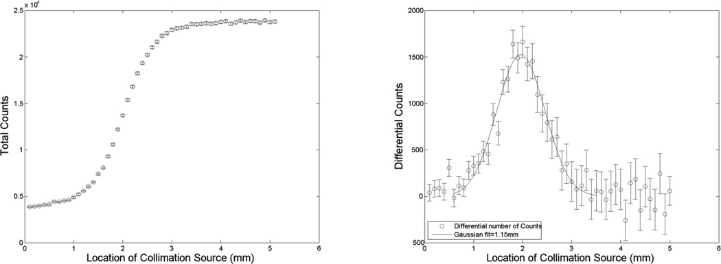
It is well known that there is a geometric uncertainty of interaction positions over the crystal depth around the center of an electronically collimated source. This geometric beam spread degrades the overall measured DOI resolution and is primarily caused by the non-zero sizes of the Na-22 source and the additional LYSO scintillator used for electronic collimation. This uncertainty of electronic collimation has been conventionally estimated from the geometry of experimental setup [4, 6, 7, 12]. In this study, we directly measured this uncertainty by scanning the same collimated Na-22 source along the edge of the crystal in 0.1 mm steps along the depth from where the count-rate was minimal caused mainly by random coincident events to where the count-rate was stable with respect to source positions, a method first investigated by Burr et al [13]. Fig. 5a shows the counts collected over 15 minutes at each source position as a function of source positions. This measured count curve is the convolution of the detection efficiency at the edge of the crystal with the geometric beam spread. Since the detection efficiency is a simple step function for a rectangular crystal, a simple derivative of the measured count curve gives the gamma interaction distribution along the depth (Fig. 5b). The uncertainty of electric collimated interactions over the depth was 1.2 mm (FWHM, with a Gaussian fit), which was then quadratically subtracted from all measured DOI resolutions to yield the final DOI resolution from detector response only.
Fig. 5.
Left: Total number of counts at each source location collected for 15 minutes at each point, with 0.1 mm step size. Right: Geometric beam spread for DOI measurements, which shows the count differences between neighboring points with 0.1 mm apart in the plot. The solid line is a Gaussian fit to these data, and has a FWHM of 1.2 mm.
3. Results
We present detailed results of DOI, energy and coincidence timing resolutions measured from crystals with representative surface finishes and geometries, and then summary results from all crystals.
3.1 Selected Crystals
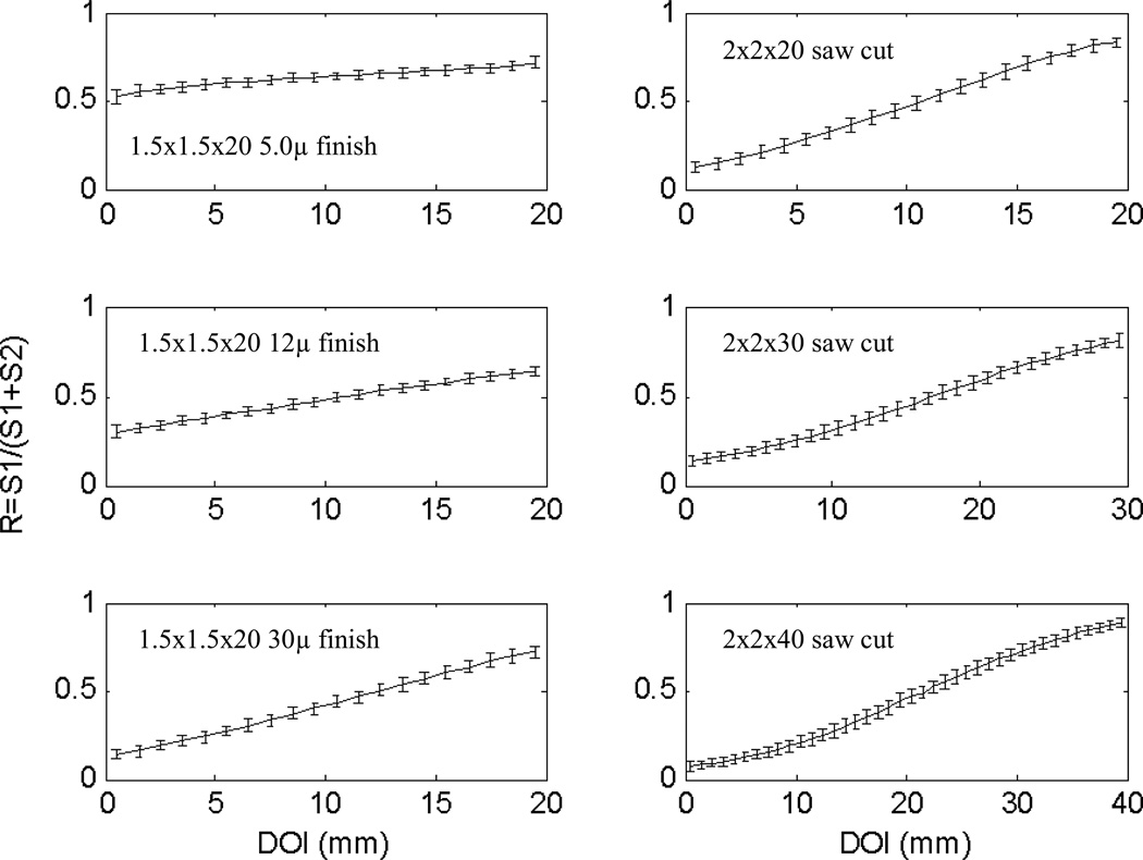
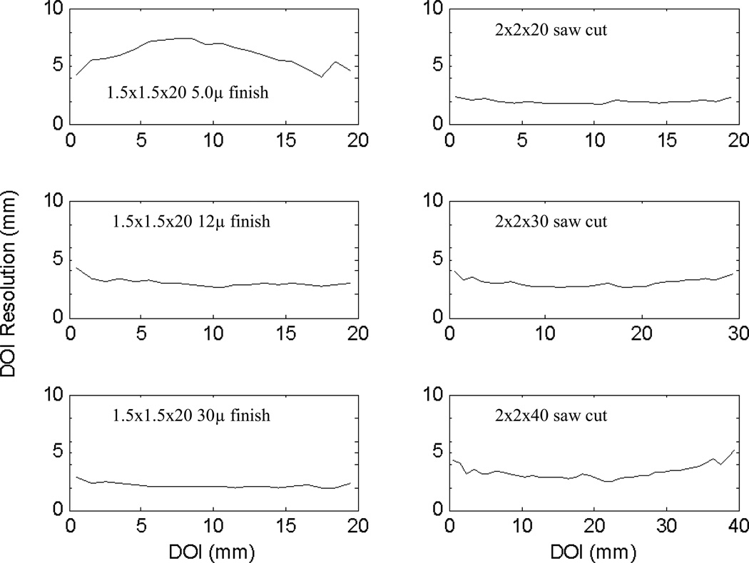
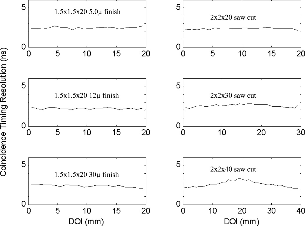
The six LYSO crystals with detailed results are: 2×2×20 mm3 with 5 µm, 12 µm and 30 µm finishes produced with lapping film, and 2×2×20 mm3, 2×2×30 mm3 and 2×2×40 mm3 with saw cut finishes produced by the manufacturer. The corresponding DOI response functions, depth dependent DOI resolutions, depth dependent coincidence timing resolution, and depth dependent energy resolution along the crystal length are shown in Fig. 6, 7, 8, and 9 respectively.
Fig. 6.
DOI response functions from 6 crystals across full depth profile. Left (top to bottom): 2×2×20 mm3 crystals with 5, 12 and 30µm finishes. Right (top to bottom): 2×2×20 mm3, 2×2×30 mm3 and 2×2×40 mm3 crystals with a saw cut finish.
Fig. 7.
DOI resolutions from 6 crystals across full depth profile. Left (top to bottom): 2×2×20 mm3 with 5, 12 and 30 µm finishes. Right (top to bottom): 2×2×20 mm3, 2×2×30 mm3 and 2×2×40 mm3 crystals with a saw cut finish.
Fig. 8.
Coincidence timing resolutions from 6 crystals across full depth profile. Left (top to bottom): 2×2×20 mm3 with 5, 12 and 30 µm finishes. Right (top to bottom): 2×2×20 mm3, 2×2×30 mm3 and 2×2×40 mm3 crystals with a saw cut finish.
Fig. 9.
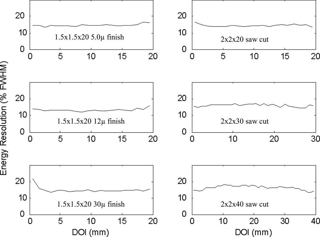
Energy resolutions from 6 crystals across full depth profile. Left (top to bottom): 2×2×20 mm3 with 5, 12 and 30 µm finishes. Right (top to bottom): 2×2×20 mm3, 2×2×30 mm3 and 2×2×40 mm3 crystals with a saw cut finish.
The DOI response function increases in slope both as the surface roughness increases and as the crystal length increases. It is noted that the DOI response function is linear over the full crystal depth with shallow slopes, and more toward to sigmoidal with steeper slopes.
The DOI resolution follows expected patterns with more highly polished crystals displaying poorer DOI resolution. Among the 2×2×20 mm3 crystals the DOI resolution varies from 7.3 mm for the 5µm finish to 2.6 mm and 2.0 mm for the 30 µm and saw cut finishes respectively. One interesting trend to note is the improvement in the DOI resolution at the edge of the crystal for the 5 µm finish caused by the sharp physical edge. That is, a spread in R that would correspond to a 10 mm resolution at the center of the crystal would cause only a 5 mm uncertainty at the edge, since the events could not take place outside the crystal. Also, note the slight degradation in the DOI resolution at the edge of the 2×2×40 mm crystal. This degradation occurs in the flat region of the DOI response function.
The energy resolution is uniform across all crystals at all depths. We observe no trends with either crystal surface finish or geometry in these crystals. All crystals vary within a region from 10% to 20% energy resolution centered at 15%.
The timing response appears similar for all crystals displayed except the 2×2×40 mm3 crystal. That is, the variation between various surface finishes is within the error of the measurement (0.24 ns), although a slight degradation with geometry is noticeable. The timing resolution is ~2.1 ns for all crystals with the exception of the 2×2×40 mm3 crystal which has a maximum timing resolution of 3.3 ns, and its degradation in timing resolution is not uniform over the length of the crystal but is strongest in the central region.
3.2 Summary Results of all individual LYSO scintillators
A summary of the depth dependent DOI, energy, and coincidence timing resolution for the full length of all 16 test crystals is given in Table I.
Table I.
Summary of measured detector performance of all crystals. The timing of the 1.5×1.5×40 mm3 crystal is unreliable at the central depth region, and the 6 ns is a conservative estimate of the worst timing resolution for that crystal.
| Crystal Properties | DOI Resolution (mm) |
Energy Resolution (%) |
Timing Resolution (ns) |
Peak Shifting (%) |
|||||||||
|---|---|---|---|---|---|---|---|---|---|---|---|---|---|
| Geometry (mm) |
Surface Finish |
Mean | Max | Min | Mean | Max | Min | Mean | Max | Min | Mean | Max | |
| 1.5×1.5×20 | saw cut | 1.5 | 2.0 | 1.2 | 17 | 19 | 15 | 2.6 | 2.9 | 2.1 | 15.4 | 26.4 | |
| 1.5×1.5×20 | 30 µm | 1.6 | 2.2 | 1.4 | 14 | 16 | 13 | 2.2 | 2.5 | 2.0 | 2.3 | 4.1 | |
| 1.5×1.5×20 | 12 µm | 2.6 | 3.0 | 2.2 | 14 | 21 | 13 | 2.4 | 2.6 | 2.2 | 2.2 | 5.8 | |
| 1.5×1.5×20 | 9 µm | 2.2 | 2.8 | 1.9 | 13 | 14 | 13 | 2.3 | 2.4 | 2.0 | 2.4 | 4.6 | |
| 1.5×1.5×20 | 5 µm | 3.3 | 4.4 | 2.1 | 14 | 16 | 13 | 2.4 | 2.6 | 2.2 | 2.9 | 7.0 | |
| 1.5×1.5×20 | 0.5 µm | 5.8 | 7.8 | 2.5 | 15 | 18 | 14 | 2.4 | 2.7 | 2.2 | 7.8 | 12.3 | |
| 2.0×2.0×20 | saw cut | 1.6 | 2.1 | 1.2 | 14 | 16 | 13 | 2.3 | 2.5 | 2.1 | 2.1 | 3.8 | |
| 2.0×2.0×20 | 30 µm | 1.8 | 2.7 | 1.5 | 15 | 22 | 14 | 2.4 | 2.6 | 2.1 | 1.7 | 2.9 | |
| 2.0×2.0×20 | 12 µm | 2.8 | 4.1 | 2.4 | 13 | 16 | 12 | 2.2 | 2.4 | 2.1 | 2.3 | 4.7 | |
| 2.0×2.0×20 | 9 µm | 3.7 | 4.1 | 2.8 | 14 | 18 | 13 | 2.3 | 2.6 | 2.1 | 1.0 | 3.4 | |
| 2.0×2.0×20 | 5 µm | 5.9 | 7.3 | 3.9 | 15 | 16 | 14 | 2.4 | 2.7 | 2.2 | 4.3 | 6.0 | |
| 2.0×2.0×20 | 0.5 µm | 7.6 | 9.9 | 3.6 | 16 | 21 | 14 | 2.4 | 2.7 | 2.2 | 7.9 | 10.5 | |
| 1.5×1.5×30 | saw cut | 2.4 | 3.9 | 1.9 | 18 | 21 | 15 | 3.3 | 5.2 | 2.2 | 23.8 | 40.1 | |
| 1.5×1.5×40 | saw cut | 4.3 | 6.9 | 2.7 | 23 | 29 | 16 | -- | 6.0* | 2.5 | 36.6 | 57.9 | |
| 2.0×2.0×30 | saw cut | 2.8 | 3.9 | 2.3 | 16 | 17 | 14 | 2.6 | 2.8 | 2.2 | 11.1 | 19.1 | |
| 2.0×2.0×40 | saw cut | 3.1 | 5.1 | 2.2 | 16 | 18 | 13 | 2.6 | 3.3 | 2.0 | 18.0 | 31.2 | |
In general, both the energy and timing resolutions measured from all scintillators with different geometries and surface finishes were good with only small differences among them except those scintillators with significant scintillation light loss as indicated by substantial photopeak shifting values. Specifically the timing resolution degrades slightly for the 1.5×1.5×20 mm3 and 2×2×30 mm3 saw cut crystals, and more noticeably for the 1.5×1.5×30 mm3 and 2×2×40 mm3 saw cut crystals. The 1.5×1.5×40 mm3 saw cut crystal has only a lower limit on the timing resolution. For this crystal the timing degradation was so severe that the peak extended outside the 20 ns timing window at many locations, and so could not be measured accurately. The saw cut crystals show the well known fact that there is strong correlation between light collection and energy and timing performance, with crystals having greater light loss producing poorer energy and timing resolutions.
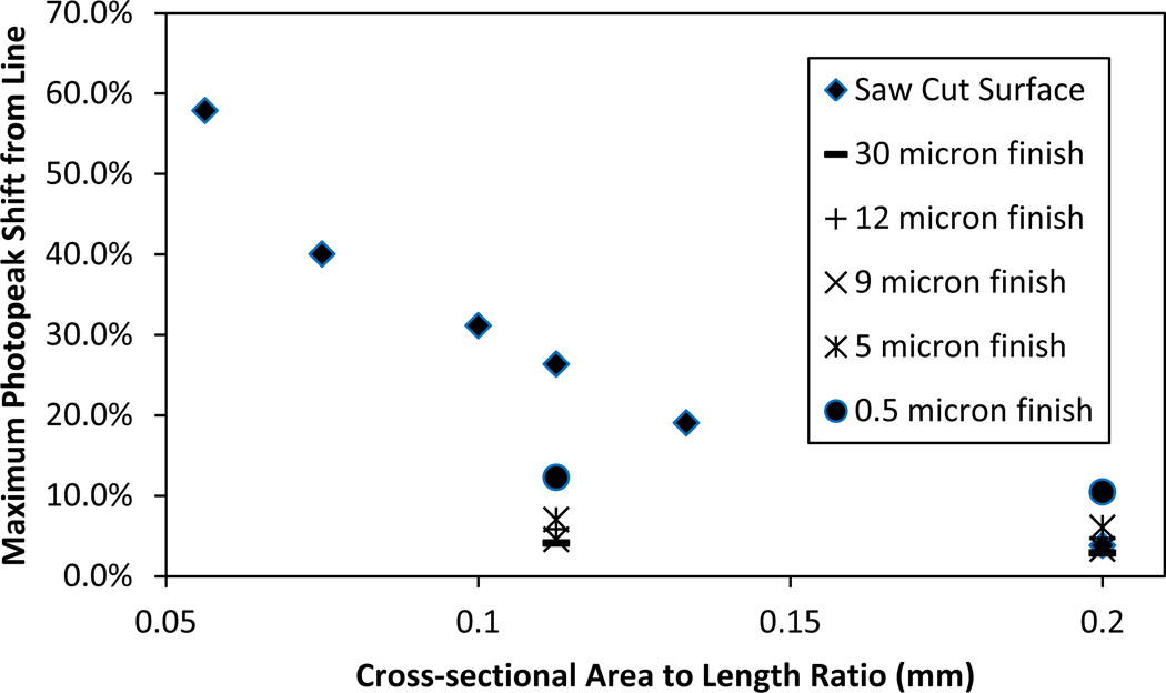
One feature to note is that all crystals with severe light loss are those with manufacturer produced surface finishing, either 0.5 µm polished or saw cut, as shown in Fig 10. Notice that the greatest light loss in the 1.5×1.5×20 mm3 crystals is from the saw cut crystals, followed by the 0.5 µm highly polished crystals. However, there is no significant light loss among the crystals of the same geometry but finished with different grades of lapping film at our lab.
Fig. 10.
Light loss comparison among crystals as a function of different geometry (cross-sectional area vs length) and surface finishes. Crystals with 0.5 µm and saw cut finishes were prepared by the manufacturer (solid dots and diamonds), while the remainders were prepared at our lab with lapping films. Note the tight grouping of all crystals prepared through lapping film regardless of surface roughness.
4. Discussion and Conclusion
In this study, only DOI resolutions of single LYSO scintillation crystals were analyzed, and so array effects such as optical crosstalk, Compton scatter, and light capture by adjacent crystals within an array were not measured. Nevertheless, single scintillator studies provide a simple, convenient and effective approach to explore different surface finishes and understand their correlation with DOI resolution and overall detector performance. This knowledge is essential to the development and evaluation of a full and expensive scintillator array. This study focused mainly on scintillators with 1.5×1.5 and 2×2 mm2 cross sections and 20 mm length due to limited resources and the suitability of these sizes to high resolution PET scanners.
This study has demonstrated that 1.5×1.5×20 mm3, and 2×2×20 mm3 crystals of any surface finish, coupled to SiPM arrays generate appropriate energy and timing resolutions for PET applications. The surface treatment does not significantly affect the energy and timing resolutions in these shorter crystals, but does change the DOI response function and DOI resolution. In crystals with a more extreme cross sectional area to length ratio light loss is observable as demonstrated by the photopeak shifting of the sum signals, and energy and timing degradations follow the light loss. That is, crystals with more significant light loss demonstrate greater timing and energy resolution degradation than crystals with more uniform light output, and depths within a crystal with greater light loss demonstrate more severe energy and timing degradations compared to depths of the same crystal with higher light output. Also, the trend is that the most measurable changes along a crystal length is first the light loss, followed by timing degradation, then by energy degradation, indicating that the light loss is a leading or most sensitive indicator of detector performance changes with different crystal properties.
For DOI measurement with DES readout techniques, it is essential to optimize the scintillator surface finish in order to achieve good DOI resolution without significantly degrading the other detector performance parameters, mainly the energy and coincident timing resolutions. An ideal crystal will keep the photopeak signal level, as calculated in Eq. (2), constant along the axial length, yet vary the ratio defined in Eq.(3) significantly over different DOI positions. However, previous studies had shown that rough surface finishes did improve the DOI resolutions but in some cases reduced the energy and coincident timing resolutions [7, 12]. However, in these previous studies an acid etching of less than one minute had significant effects on light output, even though this short time does not appear to have a noticeable effect on the DOI resolution. Similarly, this study has shown that the timing and energy resolutions are relatively uniform across the crystal length for crystal surfaces finished by lapping films with different surface roughness.
Notice in Fig. 10 the clear trend of light loss as a function of the cross-sectional area to length ratio for the saw cut crystals. The effect is less severe in the manufacturer polished crystals, but any such trends are smaller than the sensitivity of the measurement for all crystals finished by lapping films with different surface roughness. This indicates that light loss is not strongly correlated to the roughness of the surface among our samples, but arises from some different causes. We believe that the nature of large scale crystal preparation machining, even when adapted to single crystal preparation, leaves surface defects or residues that are difficult to detect but can cause minor light absorption. The light loss may be caused either by surface contamination with particles or chemicals that are difficult to remove, or by a chemical reaction between the crystal and lubricating liquid during the crystal preparation process. In our opinion the latter is more likely, since subsequent crystal surface cleaning did not affect light loss. Even if the light absorption is on the order of 2%, half of the light will be absorbed in 34 reflections, a number of reflections that is highly possible in long narrow crystals. In the study by Yang et al, the light absorption in both polished and saw-cut LYSO crystal arrays is nearly identical [6]. Similarly, Shao et al demonstrated in a previous work that a large improvement in the light collection properties of acid etched crystals after 1 minute, with no improvement in light collection with further etching [7]. Similar results were shown in energy resolution studies with single-ended-scintillator readout, thus increased surface effects due to longer average path length of light propagation by both Slates et al and Huber et al [14, 15]. Taken together, these seem to indicate that the substantial improvement in crystal performance could be achieved regardless of its surface roughness by mitigating surface defects caused during the manufacturing process. This warrants further careful studies of the exact cause of light absorption in saw cut crystals, and whether manufacturing processing can be adapted to mitigate the effect of extra light loss.
In conclusion, this study has shown that SiPM based DES readout of crystals with a surface finished with a 30 micron lapping film combined with air gap and multi-layers external defuse reflectors generates good energy, coincident timing and DOI resolutions simultaneously. For the scintillators used in this study, we found that the mean and variations of energy and timing resolutions over the crystal depth were approximately the same across various scintillator geometries and surface finishes as long as there is no significant light loss, while the DOI resolution changed considerably with different surface finishes. Further work investigating the best method to improve crystal preparation may allow the use of very long and thin saw cut crystals for improving detection efficiency, since the light collection appears to be much more dependent on surface preparation than on surface roughness.
Acknowledgment
We gratefully acknowledge the assistance of Dr. Xishan Sun for setting up the experimental study, and Keith Vaigneur at Agile Technologies for providing the scintillators used in this work. This work was supported by award R21EB007581 from the National Institute of Biomedical Imaging and Bioengineering and an Institutional Research Grant (IRG) from The University of Texas M.D. Anderson Cancer Center.
Footnotes
Publisher's Disclaimer: This is a PDF file of an unedited manuscript that has been accepted for publication. As a service to our customers we are providing this early version of the manuscript. The manuscript will undergo copyediting, typesetting, and review of the resulting proof before it is published in its final citable form. Please note that during the production process errors may be discovered which could affect the content, and all legal disclaimers that apply to the journal pertain.
References
- 1.Bruyndonckx P, Leonard S, Tavernier S, et al. Neural network-based position estimators for PET detectors using monolithic LSO blocks. Nuclear Science, IEEE Transactions on. 2004;51(5):2520–2525. [Google Scholar]
- 2.Murayama H, Ishibashi I, Uchida H, et al. Depth encoding multicrystal detectors for PET. Nuclear Science, IEEE Transactions on. 1998;45(3):1152–1157. [Google Scholar]
- 3.Bartzakos P, Thompson CJ. A depth-encoded PET detector. Nuclear Science, IEEE Transactions on. 1991;38(2):732–738. [Google Scholar]
- 4.Moses WW, Derenzo SE. Design studies for a PET detector module using a PIN photodiode to measure depth of interaction. Nuclear Science, IEEE Transactions on. 1994;41(4):1441–1445. [Google Scholar]
- 5.Yamaya T, Mitsuhashi T, Matsumoto T, et al. A SiPM-based isotropic 3D PET detector X'ta; cube with a three-dimensional array of 1 mm3 crystals. Phys Med Biol. 2011;56:6974–6807. doi: 10.1088/0031-9155/56/21/003. [DOI] [PubMed] [Google Scholar]
- 6.Yang Y, Dokhale PA, Silverman RW, et al. Depth of interaction resolution measurements for a high resolution PET detector using position sensitive avalanche photodiodes. Phys Med Biol. 2006;51:2131–2142. doi: 10.1088/0031-9155/51/9/001. [DOI] [PubMed] [Google Scholar]
- 7.Shao Y, Meadors K, Silverman RW, et al. Dual APD array readout of LSO crystals: optimization of crystal surface treatment. Nuclear Science, IEEE Transactions on. 2002;49(3):649–654. [Google Scholar]
- 8.Herbert DJ, Saveliev V, Belcari N, et al. First results of scintillator readout with silicon photomultiplier. Nuclear Science, IEEE Transactions on. 2006;53(1):389–394. [Google Scholar]
- 9.Janecek M, Moses WW. Optical reflectance measurements for commonly used reflectors. IEEE Trans Nucl Sci. 2008;55(4) [Google Scholar]
- 10.Shao Y, Li H, Gao K. Initial experimental studies of using solid-state photomultiplier for PET applications. Nucl. Instr. Meth. 2007;A 580:944–950. [Google Scholar]
- 11.Miyaoka RS, Lewellen TK, Yu H, et al. Design of a depth of interaction (DOI) PET detector module. Nuclear Science, IEEE Transactions on. 1998;45(3):1069–1073. [Google Scholar]
- 12.Zhang J, Fourdray A, Olcott P, et al. Performance characterization of a novel thin position-sensitive avalanche photodiode for 1 mm resolution positron emission tomography. Nuclear Science, IEEE Transactions on. 2007;54(3):415–421. doi: 10.1109/TNS.2007.894129. [DOI] [PMC free article] [PubMed] [Google Scholar]
- 13.Burr KC, Ivan A, Castleberry DE, et al. Evaluation of a prototype small-animal PET detector with depth-of-interaction encoding. Nuclear Science, IEEE Transactions on. 2004;51(4):1791–1798. [Google Scholar]
- 14.Slates R, Charziioannou A, Fehlberg B, et al. Polishing of LSO crystals to increase light output. Nuclear Science, IEEE Transactions on. 2000;47(3) [Google Scholar]
- 15.Huber JS, Moses WW, Andreaco MS, et al. Geometry and surface treatment dependence of the light collection from LSO crystals. Nucl. Instr. Meth. 1999;A 437:374–380. [Google Scholar]


