Abstract
Integration of nano-materials in optical microfluidic devices facilitates the realization of miniaturized analytical systems with enhanced sensing abilities for biological and chemical substances. In this work, a novel method of integration of gold nano-islands in a silica-on-silicon-polydimethylsiloxane microfluidic device is reported. The device works based on the nano-enhanced evanescence technique achieved by interacting the evanescent tail of propagating wave with the gold nano-islands integrated on the core of the waveguide resulting in the modification of the propagating UV-visible spectrum. The biosensing ability of the device is investigated by finite-difference time-domain simulation with a simplified model of the device. The performance of the proposed device is demonstrated for the detection of recombinant growth hormone based on antibody-antigen interaction.
INTRODUCTION
Bovine growth hormone, also known as bovine somatotropin (bST) is a growth promoter widely used in some countries in dairy farming for increasing the production of milk and meat. With the injection of hormone to animals, the milk production has been reported to be increased more than 5% to 40%.1, 2, 3 The commercial use of growth hormone was made possible with the discovery of recombinant DNA technology, which could produce large amounts of artificial growth hormone called recombinant bovine somatoropin (rbST) using hybridization technique. The use of rbST in dairy farming is still controversial due to its potential effects on the health of cattle and consumers.4, 5, 6 Therefore, a rapid and precise method of detection of rbST has a lot of demand for regulation.
The enzyme-linked immunosorbent assay (ELISA),7, 8 radioimmunoassay (RIA),9 bioassay method,10 surface plasmon resonance (SPR)11 and localized surface plasmon resonance (LSPR)-based sensor12 are reported for the detection of growth hormone. The fluorescent tagging and detection using a lab-on-a-chip platform13 and the use of a novel cascaded waveguide coupler (CWC)14 on silica-on-silicon platform are also attempted. ELISA can predict the concentration of rbST in a relative form that is based on the concentration and affinity. The liquid chromatography-mass spectrometry (LC-MS),15, 16 combined with electrospray ionization is a very powerful technique which can discriminate the natural and artificial form of the growth hormone, however, the method is complex and expensive. In this work, a miniaturized senor platform is developed for the detection of recombinant growth hormone. The sensor uses a label-free detection methods by using the LSPR property of nano-island on silica-silicon waveguide integrated in a microfluidic device.
The optical detection is one of the most widely used methods of bio-detection.17 Labeled18 and label free19, 20 detection are the two major approaches of the optical detection method. In the labeled detection, fluorescence dye molecules are tagged with biomolecules and detected in an optical microfluidics platform. Labeled detection is an expensive and time consuming process as it needs the optimization of the flurophore-biomoelcule labeling conditions, also the accuracy depends on the labeling process. As a result, label-free detection has gained increased attentions in biomedical field. The label-free detection methods reported in the literatures are autofluorescence,21 confocal Raman spectroscopy,22 surface plasmon resonance,23 localized surface plasmon resonance,20, 24 and evanescence.25, 26, 27
The SPR is a widely reported label-free detection of biological and chemical species. The SPR sensor works based on the plasmon waves produced by coupling the light to a thin layer of metal by using grating coupler or field excitation. The basic mechanism of SPR sensor is the modulation of plasmon resonance band with the adsorption of bio-species to the metal layer. Metallic nanoparticles such as gold and silver exhibit strong plasmonic property called LSPR in the ultraviolet and visible region of electromagnetic spectrum. LSPR is due to the collective oscillation of electrons of the metallic nanoparticles for a certain wavelength of light, which leads to absorption of light. The plasmonic property of the gold nanoparticle is widely reported28, 29 for the detection of biological species as the plasmonic properties of gold nanoparticles (NPs) are sensitive to the change in the refractive index of the surrounding medium. Conventionally, the biosensors reported by using metallic NPs are substrate-based.30 In this method, the NPs are immobilized on a transparent substrate and the biomolecules are adsorbed and detected by monitoring the changes of plasmon band by using the transmission or reflection spectroscopy. The advantages of LSPR based detection over the SPR detection are that there is no need of any complex light coupling optics and the feasibility of modifying the plasmonic property by tuning the shape and size of the nanoparticles.
Evanescent-wave is the exponentially decaying tail of the propagating wave in a waveguide, which can interact with bio-species immobilized on the waveguide. Evanescent wave sensors by using optical fibers31 or planar waveguides32 are reported for the labeled and label-free detection of the bio-species. For the label-free evanescent sensor, the interaction of evanescent wave with the biomolecules immobilized on the core of the waveguide results in the loss of the propagating waves due to the absorption of evanescent wave. Since the depth of penetration of evanescent wave sensor implemented by a straight waveguide having uniform diameter is less, the sensitivity is less. However, the sensitivity can be increased by increasing the species evanescent-wave interaction length. Alternatively, the sensitivity of the evanescent wave sensors was reported to be increased by techniques such as selective ray launching,33 tapering of fiber probes,26 and use of bends34 in waveguides. In this work, a novel method of integration of gold nano-islands on silica-on-silicon waveguide is used for the development of an evanescent wave senor integrated in a polydimethylsiloxane (PDMS) microfluidic chip.
Recently, the integration of nano-materials in the microfluidics environments has gained a lot of attentions due to the feasibilities of developing micro total analysis systems (μTAS) or lab-on-a-chips (LOCs) devices with higher sensitivity.35 Lab-on-a-chips are gaining increased interest because of their capability to perform biological and chemical detections with reduced consumption of reagents and materials.36, 37 Since the LOCs are miniaturized devices, they are portable and capable of performing the detection and analysis faster than the macroscopic instruments. By miniaturizing and integrating various process modules such as fluidics and optical detections components in a single chip, the LOCs have been able to perform different bio-analytical processes. Integration of microfluidics with optical components is one of the challenging tasks in the fabrication of optical LOCs. Also, the fabrication techniques of integration of nano-features in the microfluidic environments are gaining more attentions,35 because of the unique optical properties of nano-structure that are useful for the biosensing.
Miniaturizations of conventional SPR systems are reported for biosensing purpose.38, 39 Some of the commercial devices such as Biacore systems are already available with the integration of SPR sensors in microfludics, wherein a flat layer of gold is used in a Kretschmann configuration with a prism coupling of light to excite plasmon waves. However, the microfluidics based SPR system is complex and it needs complicated optics and expensive instruments. Integration of nanoparticle in the microfluidic device is a useful approach as the optical setup required for such a sensor is simple, as compared with SPR or confocal Raman spectroscopy based sensors. However, the integration of nanoparticles in microfluidics requires novel nanofabrication techniques compatible with the microfluidic fabrication process and materials.
Optical biosensors can be implemented by using both the single and multimode waveguides. Single mode waveguides are more suitable to implement biosensors with higher sensitivity. However, the coupling of light to single mode waveguide requires complex light coupling apparatus. Recently, Kayani et al.40 reported a work on a single mode sensor and suggested a novel method of manipulating the modal properties based on dielectrophoresis of randomly dispersed nanoparticles in microfluidic channel. Surface enhanced Raman scattering (SERS) of silver nanoparticles41 and nanoporous42 are also reported to be enhanced by dielectrophoresis in microfluidics device leading to the enhancement of detection sensitivity.
In this work, a nano-enhanced evanescent wave biosensor integrated with gold nano-islands on a multimode silica-on-silicon waveguide is presented. A miniaturized analytical device is developed by integrating gold nano-islands on a silica-on-silicon (SOS) waveguide. The SOS waveguide is further hybrid integrated in a microfluidic device fabricated on PDMS. As the nano-islands are on the core of the waveguide, the evanescent tail of the propagating waves interacts with the gold and changes the transmittance spectrum. The bio-species adsorbed on the gold nano features change the local refractive index of the gold, which essentially modifies the transmittance spectrum of the light propagating through the SOS waveguide, hence a nano-enhanced evanescent mechanism is achieved. The integration process of gold nano-islands on the SOS chip is compatible for the fabrication of a lab-on-a-chip. In this design, the sensor chip is integrated into a microfluidic environment by using soft lithography on PDMS for the realization of a low cost LOC. The proposed nano-integrated LOC is demonstrated for the detection of recombinant growth hormone.
In order to understand the enhancement of evanescent sensing, a simplified model of the proposed device is simulated by 3D finite-difference time-domain (FDTD) method by using the Rsoft, FullWAVE.
MATERIALS AND METHOD
Materials
Recombinant bovine somototropin (rbST, MW 22 kDa) and its antibody (Anti-bST) were received from Cedarlane, ON, Canada. The rbST diluted in phosphate buffered saline (PBS) at a concentration of 5000 ng/ml was used as stock solution and stored at 3-5 °C. The anti-bST obtained in powder form was dissolved in PBS at a concentration of 5000 ng/ml and stored in refrigerator at 3-5 °C. Hydrogen tetrachloroaurate (III) trihydrate (HAuCl4.3H2O) was received from Alfa Aesar. Sodium citrate, 11-mercaptoundecanoic acid in ethanol (Nano Thinks Acid 11), N,N’-diisopropylcarbodiimide and N-hydroxysuccinimide PBS were obtained from Sigma Aldrich, Canada. PBS dissolved in DI water at a concentration of 0.1 M and pH of 7.2. The SYLGARD184 elastomer kit and curing agent for the PDMS fabrication were obtained from Dow Corning.
Gold nano-islands integrated LOC
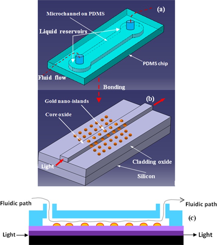
The integration process of the proposed device is illustrated in Fig. 1. The device has two main parts, one is the SOS waveguide with gold nano-islands integrated on it and the other part is a PDMS microfluidic chips. The SOS waveguide has two layers of silicon dioxide deposited on silicon substrates. The first silicon dioxide layer acts as the bottom cladding layer for the waveguide, while the second layer with higher refractive index than the cladding acts the core of the waveguide. The core layer is micromachined to certain width for the lateral confinement of light. The gold nano-islands are integrated on the core to modify the evanescent field of the waveguide due to the localized surface plasmon property of the gold nano-islands. The schematic of the SOS waveguide integrated with gold nano-islands is shown in Fig. 1b.
Figure 1.
Schematic diagram of integration process of the LOC, (a) PDMS microfluidic chip, (b) SOS optical chip integrated with gold nano-islands, and (c) sectional view of the LOC.
The PDMS chip has a microfluidic channel and two liquid reservoirs as shown in Fig. 1a. The chip is bonded with the SOS waveguide so that the bio-species can be pumped through the gold nano-islands integrated on the SOS waveguide. The fluidic tubes are fixed with the liquid reservoir to facilitate the microfluidic flow through the device. When the bio-species are adsorbed to the gold nano-islands, their bio-interaction influences the evanescent field as measured through the waveguide.
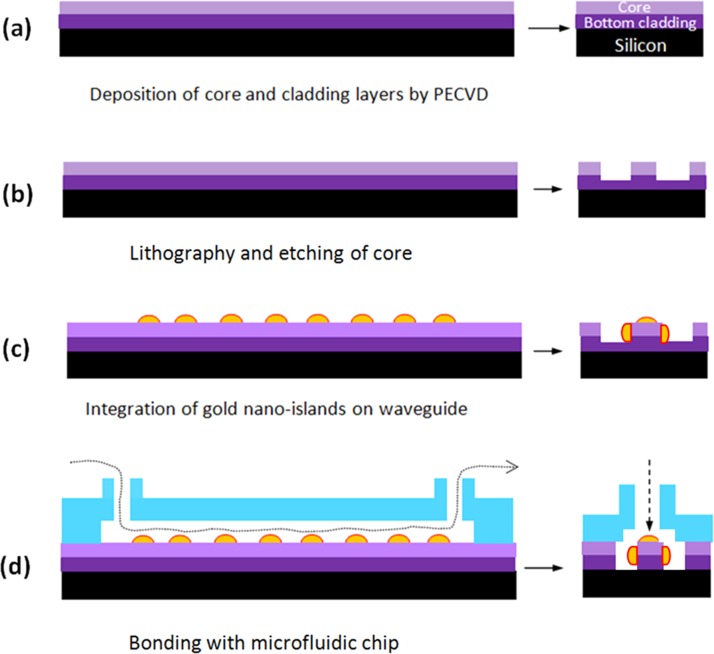
The fabrication process flow of the nano-islands integrated LOC is shown in Fig. 2. The device is fabricated on SOS waveguide. Fig. 2b shows the SOS waveguide with two layers of silicon dioxide. The first layer with lower refractive index and the second layer with higher refractive index act as the bottom cladding and core of the waveguide, respectively.
Figure 2.
Fabrication process steps of gold nano-islands integrated LOC.
Then the nano-islands are integrated on the core of the SOS waveguide by convective assembly (Fig. 2c). Subsequently, the microfluidic chip fabricated on PDMS by soft-lithography is bonded with the SOS waveguide and the LOC is realized as shown in Fig. 2d. The fabrication details of all the steps given in Fig. 2 are explained in Secs. 3–5.
FABRICATION OF SILICA-ON-SILICON OPTICAL CHIP
The fabrication of silica-on-silicon waveguide involves the deposition and micromachining of silicon dioxide layers. The plasma enhanced chemical vapor deposition (PECVD) was used for the deposition of silicon dioxide layers. For the PECVE deposition, PlasmaLab 80 Plus instrument of Oxford instruments is used. Different deposition process parameters are optimized to achieve necessary refractive indices for the cladding and core. For depositing the cladding oxide, the chamber pressure and substrate temperature were set 1000 mT and 300 °C, respectively. The gas mixture of silane and nitrogen (5% SiH4, 95% N2) was introduced to the chamber at the flow rate of 170 sccm. The nitrous oxide (N2O) was introduced to the PECVD chamber at the flow rate of 710 sccm. Then the plasma was created by RF power of 20 W at 13.56 MHz. The deposition rate was 50 nm/min. The deposition was carried out for 4 h and 30 min. The thickness of oxide layer was approximately 14 μm for the bottom cladding of the waveguide. To obtain higher refractive index for the core layer, the flow rate of the silane and nitrogen mixture and N2O was increased to 500 sccm, and the RF power was increased 200 W. The refractive indices of the silicon dioxide layers were measured by ellipsometry (Spectroscopic ellipsometer, Model: VASE, Sopra). The refractive indices for the core and cladding were 1.445 and 1.457, respectively at a wavelength of 635 nm.
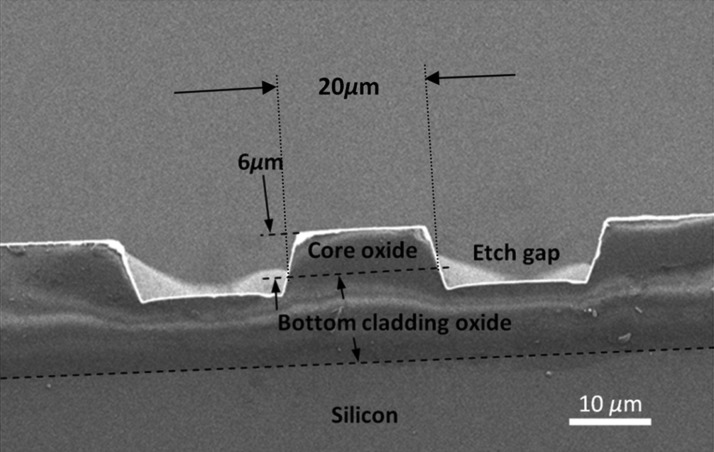
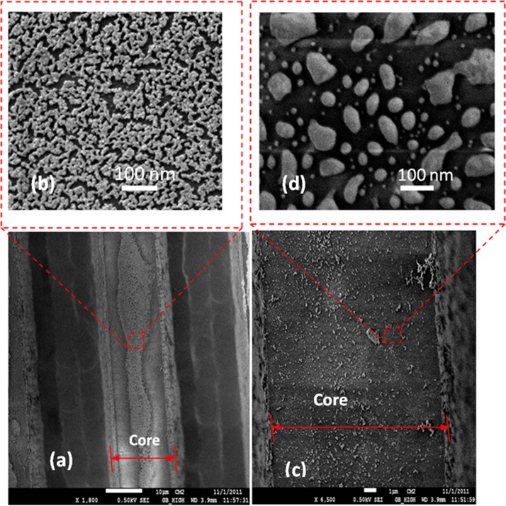
The micromachining of the core was carried out by using direct write lithography (DWL) and reactive ion etching (RIE). The mask pattern was designed in L-edit software and used in the DWL-66 laser writer and the patterns were written directly on the wafer. The DWL write head of 2 mm having a resolution of 500 nm was used. The AZ1518 photoresist was used for the lithography. The resist layer of thickness of 2 μm was spun at 3000 rpm for 30 s and baked at 110 °C for 2 h in an oven. The pattern was etched in MERIE P5000 plasma machine of applied materials. For the RIE, the chamber pressure was set to 50 mT and the process gases, CHF3, Ar and CF4 were introduced at the flow rate of 45, 70, and 7 sccm, respectively. The plasma was created by the RF power of 300 W. This process gives the etch rate of 0.3 μm/min. RIE was carried out for 1 h including the 30 min of etch pause steps to prevent the burring of photoresist, which resulted in the etch depth of the 10 μm. The SEM micrograph of the waveguide is shown in Fig. 3.
Figure 3.
SEM image of the SOS waveguide showing the sectional view of waveguide with the core and cladding dimensions.
INTEGRATION OF NANO-ISLANDS ON THE SILICA-ON-SILICON WAVEGUIDE
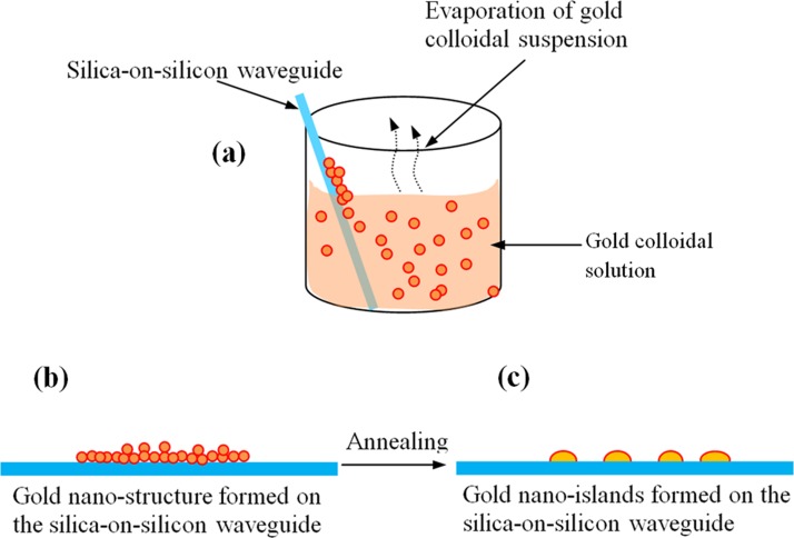
The nano-islands are integrated on the SOS waveguide using angled convective assembly12 in colloidal gold solution that was prepared by Turkevich's method.43 The spherical gold nanoparticles were absorbed to the SOS waveguide by evaporating the aqueous solution containing the gold nanoparticles as shown in Fig. 4a.
Figure 4.
Illustration of the method of integration of gold nano-islands on the silica-on-silicon optical chip. (a) SOS waveguide in gold colloidal solution, (b) gold nano-structure on the waveguide, and (c) gold nano-islands on silica-on-silicon optical chip.
The process of integration of gold nano-islands on the silica-on-silicon waveguide is illustrated in Fig. 4. Before the deposition, the SOS waveguides were cleaned with soap solution and DI water, then rinsed with acetone, dried and finally rinsed with 2-propanol. The waveguides were silanized and heated at 100 °C for 1 h and immersed in the gold colloid solution and kept in an oven at temperatures between 60 and 80 °C as shown in Fig. 4a. The solution was evaporated entirely in 2 days. During the evaporation of the aqueous solution, the gold nanoparticles from the solution drive to the surface and a nano-cluster were deposited on the waveguide (Fig. 4b). The nano-cluster morphology was transformed to nano-islands by a post deposition annealing as shown in Fig. 4c. In order to investigate the morphology of the deposited gold nanoparticle, SEM characterization was carried out. As the proposed convective assembly is not a controlled process, the morphology of the deposited layer of gold is found to be of nano-clusters as shown in Fig. 5a. A closer view of the nano-cluster formed on the waveguide is shown in Fig. 5b.
Figure 5.
SEM micrograph of gold nano-islands integrated silica-on-silicon waveguide: (a) waveguide with gold nano-cluster, (b) closer view of the nano clusters, (c) the waveguide after annealing, and (d) closer view of waveguide after annealing.
The plasmonic property of the nano-cluster formed on the glass substrate was already measured,12, 44 which showed that the nano-cluster morphology has a wide LSPR band and it was found not good for the biosensing. By using a post deposition annealing process, the morphology of the deposition was transformed to nano-islands. During the annealing, the nano-cluster melts and due to high surface tension of the molten metal, a nano-island morphology is formed as shown in Fig. 5d.
FABRICATION OF THE GOLD NANO-ISLAND INTEGRATED LOC
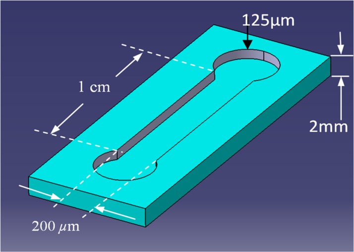
In order to fabricate the proposed device, the SOS optical chip with nano-islands was bonded with microfluidic chip. The microfluidic chip was fabricated on the PDMS using soft lithography technique. The microfluidic chips consist of a microchannel of width 200 μm and length 1 cm with two liquid reservoirs at the ends of the microchannel as shown in Fig. 6. The schematic of the microfluidic chip is shown in Fig. 6.
Figure 6.
Schematic of the microfluidic chip.
The PDMS chip was fabricated by soft lithography. A mold for casting the PDMS was fabricated by using SU8 photoresist. The mold is the negative pattern of the chip shown in Fig. 6. During the bonding of the SOS chip with PDMS chip, the core of the waveguide must be inside the microchannel, hence the width of the channel was chosen to 200 μm to simplify the aligning task during the bonding. The depth of the channel was chosen to 125 μm to avoid the possible collapsing of the channel to the core during the bonding. The mold for the microfluidic chip was fabricated by UV- photolithography on SU8 photoresist. A negative photoresist (SU8-2035 Microchem) was spun twice on a silicon substrate for 30 s at 2000 rpm to form the resist layer with thickness of 125 μm. The resist was beaked at 80 °C for 10 min after each spinning. Then the resist was exposed by UV light for 30 s through a mask. After the UV exposure, the resist was baked again and the pattern was developed in 15 min. The mold was silanized before casting the PDMS. The base and curing agent of the PDMS was mixed and degassed in a vacuum desiccator to remove the gas bubble and casted in the mold. The PDMS was cured at 80 °C for 5 h and the microfluidic chip was removed from the mold.
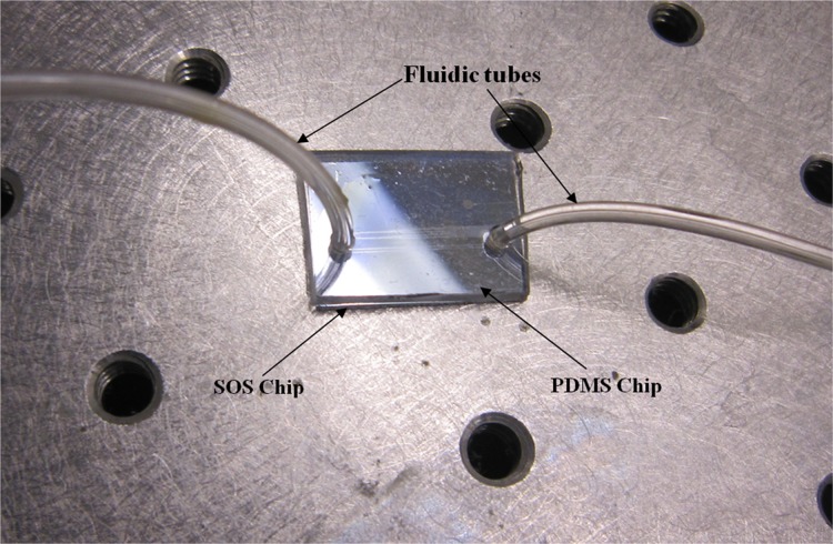
The chips were bonded by oxygen plasma techniques. The PDMS chip and the waveguide were cleaned by DI water and dried and loaded to oxygen plasma instrument. The samples were exposed to the oxygen plasma for 35 s. The bonding was carried out under a microscope to align the microfluidic channel with the waveguide. The fluidic tubes are inserted to the reservoirs and fixed to pump the bio-liquids to the device. PDMS was put on the SOS-PDMS interface to prevent the leakage through the etch gap of SOS waveguide, and immediately baked in an oven to prevent the flow of PDMS into the microchannel. Fig. 7 shows the gold nano-island integrated LOC.
Figure 7.
Gold nano-islands integrated LOC.
FDTD SIMULATION OF THE DEVICE
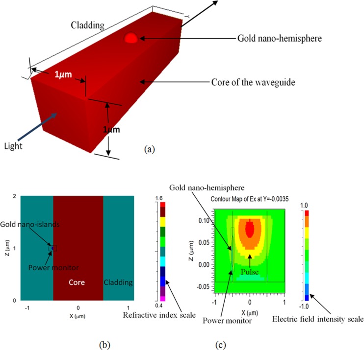
In order to investigate the effects of nano-islands on the propagation of light through the SOS optical chip, a simplified model of device is simulated by using FDTD technique. The FDTD method solves the Maxwell's differential equations by discretizing using central difference in space and time followed by solving them numerically by computers. The simulation domain is discretized into small elements called grid, and the accuracy of the FDTD computation depends on the size of the grid elements. As the simulation of real device require large computational resources, a simplified model of the device with a waveguide having the square cross section of 1 × 1 μm and a gold nano-hemisphere on the core of the waveguide is used for the FDTD simulation. The FDTD model used for the simulation is shown in Fig. 8.
Figure 8.
(a) FDTD model of the device. (b) Refractive index of the model. (c) Electric field distribution in the model.
The refractive index of the core was set to 1.46. A gold nano-hemisphere having the diameter of 70 nm is placed on the surface of the core. In order to assess the biosensing performance of the device, the refractive index of the cladding, that is, the region around the core is varied between 1 and 1.4 in the simulation. In order to compute the absorbance of the light due to the gold nano-sphere a power monitor is placed around the nano-hemisphere. An optical pulse with wavelength of 500 nm is used as the excitation source in the simulation. The power monitor placed with the nano-island can calculate the absorbance spectrum by using fast Fourier transform (FFT) algorithm.
Figs. 8b, 8c show the refractive index distribution of the model and the FDTD simulation showing the propagation of pulse through the waveguide. Fig. 8c shows the electric field distribution in the model computed by FullWAVE during propagation of light pulse.
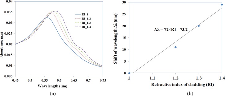
Fig. 9 shows the FDTD simulation results of the gold nano-islands integrated device. Fig. 9a shows the absorbance spectra of the gold nano-island with diameter of 70 nm located on the surface of the core of the waveguide. As the evanescent filed of the light propagating through the waveguide is extending to the cladding, the gold nano-island located at the core-cladding interface are excitated by the evanescent field, which results in a collective oscillation of electrons of the gold nano-island at certain wavelengths and the absorption of light. This phenomenon is referred to as LSPR. The Fig. 9a shows the LSPR spectrum of the gold nano-islands by the excitation of evanescence field. The LSPR peak was measured at 560 nm when the cladding index was 1. The LSPR is sensitive to the local refractive index of the gold nano-island. The simulations carried out by changing the cladding index to 1.2, 1.3, and 1.4 showed that LSPR peak is shifting to higher wavelength and also the band is becoming wider as shown in Fig. 9a. The intensity of the LSPR band is also found increasing with the refractive index. A linear trend in the shift of LSPR peak against the refractive index is observed as presented in Fig. 9b. The sensitivity of the device against the refractive index is measured as 72 nm/RIU, which is the slope of the trend line in Fig 9b.
Figure 9.
(a) LSPR spectrum of the gold nano-island integrated on the core of the SOS waveguide and (b) shift of LSPR peak wavelength against the refractive index of the cladding of the SOS waveguide.
The figure of merit (FoM) of the sensor is estimated as the ratio of the refractive index sensitivity to the spectral width of the absorbance spectrum of the gold nano-islands as explained in Ref. 45. Since the absorbance spectrum of the gold nano-islands is an asymmetrical spectrum, the spectral width is measured at 90% of the absorbance peak as 65 nm. The FoM of the device is estimated as 1.107.
The FDTD simulation demonstrates that the nano-island integrated waveguide is useful for the biosensing applications. During the biosensing, the bio-species are adsorbed to the gold nano-islands and the local refractive index changes, hence the spectrum of the propagating light modifies, is the basic mechanism of the proposed device.
EXPERIMENTAL SETUP OF NANO-ISLANDS INTEGRATED LOC
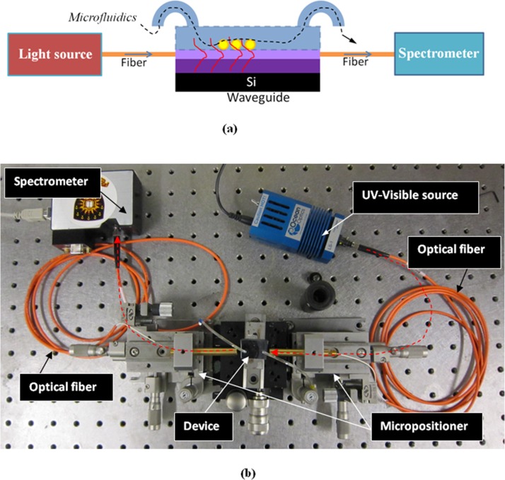
The schematic and photograph of the experimental setup of the device are shown in Fig. 10. The setup includes an UV-visible source, device under test (DUT) and spectrometer as shown in Fig. 10a. Light from the UV-visible source (Ocean optics LS-1) is coupled to the SOS waveguide through a fiber using a high precision micropositioners. The device is fixed in single axis controllable stage between the two 5 axis controllable micropositioner stages. Similarly, spectrometer (Ocean Optics USB 2000) is coupled to the output side of the waveguide using a multimode fiber as shown in Fig. 10b.
Figure 10.
Testing setup for nano-enhanced evanescence measurement: (a) schematic of the experimental setup and (b) photograph of the experimental setup.
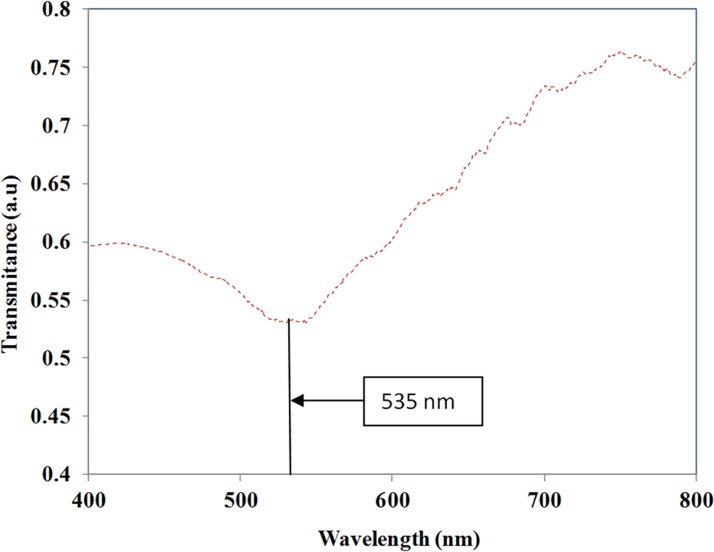
Before starting the bio-sensing experiments in the device, a device without nano-islands was fixed in the setup and a reference spectrum corresponds to the source signal was recorded by the spectrometer. This reference spectrum was used for measuring the transmittance spectrum of the nano-islands integrated LOC. PBS solution was pumped to the device during all the measurements. After taking the reference spectrum, the nano-island integrated LOC was fixed to the measurement setup. The transmittance spectrum recorded from nano-island integrated LOC is shown in Fig. 11.
Figure 11.
Transmittance spectrum recorded in the nano-island integrated LOC.
Fig. 11 shows the transmittance spectrum of the light propagating through the device. When the UV-visible light was coupled to the device, due to interaction of evanescent waves with gold nano-island, certain wavelengths are absorbed by the localized surface plasmon resonance of the gold nano-island. Minimum transmittance was observed in the transmittance spectrum at 535 ± 10 nm for the measurements taken in 10 devices. The transmission minimum corresponds to the absorbance peak due to the LSPR of the gold nano-islands.
BIOSENSING
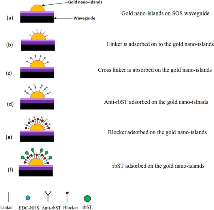
Biosensing experiments are carried out by pumping the reagents and rbST solutions to the device. Fig. 12 illustrates various steps in the detection of recombinant growth hormone. Before starting the experiments, de-ionized water was pumped to the device for 1 min to clean the device.
Figure 12.
Steps used in the detection of rbST in the nano-islands integrated LOC.
Fig. 12a represents gold nano-islands on the silica-on-silicon waveguide in the microfluidic device. Then the linker solution, mercaptoundecanoic acid in ethanol was pumped to the device and kept for 1 h and washed by passing PBS for 10 s. Fig. 12b shows sample after passing the linker solution. Then the cross-linker solution (N, N′-diisopropylcarbodiimide and N-hydroxysuccinimide (EDC-NHS)) was pumped and kept for 1 h and washed by pumping PBS solution for 10 s. The linker and cross-linker modify the surface of the gold so that the biomolecules can be attached to the gold. Fig. 12c shows the gold nano-island after pumping the cross-linker. Then the antibody (ant-rbST) was pumped to the device and kept for 1 h followed by washing in PBS. Fig. 12d represents the sample after anti-rbST was adsorbed to the gold nano-hemisphere. Then the transmittance spectrum was measured after anti-rbST was adsorbed to the gold nano-island. During the measurement of transmittance spectrum, PBS solution was filled in the microchannel. In order to prevent the non-specific binding of rbST to the gold nano-islands, a blocker solution prepared from the non fat milk powder was used. The milk solution (1%) was pumped to the device and kept for 1 h and washed with PBS. Fig. 12e represents the sample after the blocker solution was adsorbed to the sample. Finally, the rbST was pumped to the device and kept for 1 h and washed with PBS (Fig. 12d). Then the transmittance spectrum was recorded with PBS filled in the microchannel. The red shift of the transmittance minimum from the step (d) to (f) is estimated as a measure of the antigen-antibody interaction of the rbST. The sensitivity of the device was investigated for various concentration of rbST.
RESULTS AND DISCUSSION
The antibody-antigen interaction of rbST that occurs on the gold nano-islands and waveguide change the refractive index and/or the thickness of the biolayer absorbed on the gold nano-island. The change of local refractive index modifies the plasmonic band of the gold nano-islands. The shift of the plasmonic band is used as a measure of the antibody-antigen interaction of rbST. In the present work, the transmittance spectrum of the light propagating through the device is analyzed to detect rbST. Fig. 13 shows the transmittance spectrum recorded at various steps of the biosensing process.
Figure 13.
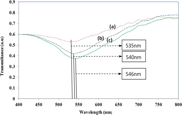
Change of transmittance spectrum against the antibody-antigen interaction of rbST, (a) spectrum with gold nano-islands on the waveguide, (b) spectrum after antibody (anti-rbST: 100 ng/ml) is absorbed to the gold nano-islands, and (c)spectrum after antigen (rbST: 800 ng/ml) is absorbed to gold nano-islands.
Fig. 13a shows the transmittance spectrum recorded before starting the biosensing process. The spectrum with minimum transmittance recorded at 535 nm corresponds to the absorbance peak of the gold nano-islands integrated on the waveguide. The spectrum was shifted to 540 nm after the antibody of a concentration of 100 ng/ml was immobilized to the gold nano-islands. The band is found to become wider as shown in Fig. 13b. Fig. 13c shows the spectrum recorded after rbST at a concentration of 800 ng/ml interacted with antibody immobilized on the gold nano-islands. The band became wider and also the transmittance minimum was further red shifted to 546 nm. A red shift of 6 nm in the transmittance spectrum is due to the modification of LSPR property of the gold nano-islands due to the interaction of the anti-rbST and rbST.
The suitability of the sensor for the quantitative measurements of rbST is investigated with various concentrations of rbST. The concentration of the anti-rbST was kept at 100 ng/ml and concentration of rbST is varied between 10 and 800 ng/ml.
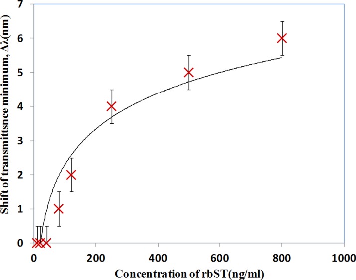
Fig. 14 shows the tested variation of the shift of minimum transmittance against the concentration of the rbST. Variation of shift in the transmittance spectrum can be observed as shown in Fig. 14. The sensor response is found slightly saturating after 500 ng/ml. A shift of 1 nm is observed when the concentration of rbST was reduced to 80 ng/ml. The minimum concentration of the rbST that was detected in the present device is 80 ng/ml. A trend line is fitted to the data in Fig. 14 and the limit of detection is measured at the point where the trend line crosses the concentration axis. The limit of detection of the device is estimated to be as low as 20 ng/ml.
Figure 14.
Effect of concentration of rbST on the shift of minimum transmittance due to antibody-antigen interaction of rbST.
The concentration of bST in milk is reported to be of the order of 1-10 ng/ml.46 The rbST may be found in the milk of the cattle treated with rbST, and concentration of rbST present in the milk may be of the order of hundreds of ng/ml,47 depending on the quantity of the rbST used for the production of milk. Hence the proposed device is suitable for the detection of rbST in milk.
CONCLUSION
A lab-on-a-chip is developed by integrating gold nano-islands on the silica-on-silicon waveguide and PDMS microfluidic chips. The device works based on the modification of transmittance spectrum due to the absorption of light by the enhanced evanescence due to the gold nano-islands. The transmittance spectrum is modified due to the interaction of evanescent field of the propagating light with the gold nano-island. The device is demonstrated for the detection of recombinant growth hormone. The effect of concentration of rbST on the shift of transmittance spectrum is investigated and the detection limit of the device is estimated. The detection limit of the device is found to be 20 ng/ml.
ACKNOWLEDGMENTS
Authors would like to thank Ministère du Développement économique, innovation et exportation (MDEIE) Québec and Valeo Gestion, Montreal, Canada for the financial support for the project.
References
- Burton J. H. et al. , “ Overall efficacy of chronically administered recombinant bovine somatotropin to lactating dairy cows,” J. Dairy Sci. 73(8 ), 2157–2167 (1990). 10.3168/jds.S0022-0302(90)78896-0 [DOI] [PubMed] [Google Scholar]
- McBride B. W. et al. , “ Use of recombinant bovine somatotropin for up to two consecutive lactations on dairy production traits,” J. Dairy Sci. 73(11 ), 3248–3257 (1990). 10.3168/jds.S0022-0302(90)79017-0 [DOI] [PubMed] [Google Scholar]
- Etherton T. D. and Bauman D. E., “ Biology of somatotropin in growth and lactation of domestic animals,” Physiol. Rev. 78(3 ), 745–761 (1998). [DOI] [PubMed] [Google Scholar]
- Buttel F. H., “ The recombinant BGH controversy in the United States: Toward a new consumption politics of food?,” Agric. Human Values 17(1 ), 5–20 (2000). 10.1023/A:1007636911210 [DOI] [Google Scholar]
- Burkhardt J., “ On the ethics of technical change: The case of bST1,” Technol. Soc. 14(2 ), 221–243 (1992). 10.1016/0160-791X(92)90005-U [DOI] [Google Scholar]
- Molnar J. J., Cummins K. A., and Nowak P. F., “ Bovine somatotropin: Biotechnology product and social issue in the United States Dairy Industry,” J. Dairy Sci. 73(11 ), 3084–3093 (1990). 10.3168/jds.S0022-0302(90)78996-5 [DOI] [Google Scholar]
- Castigliego L. et al. , “ Natural and recombinant bovine somatotropin: Immunodetection with a sandwich ELISA,” J. Dairy Res. 74(01 ), 79–85 (2007). 10.1017/S0022029906002159 [DOI] [PubMed] [Google Scholar]
- Zhao X. et al. , “ Somatotropin and insulin-like growth factor-I concentrations in plasma and milk after daily or sustained-release exogenous somatotropin administrations,” Domest. Anim. Endocrinol. 11(2 ), 209–216 (1994). 10.1016/0739-7240(94)90028-0 [DOI] [PubMed] [Google Scholar]
- Groenewegen P. P. et al. , “ Bioactivity of milk from rbST treated cows,” J. Nutr. 120, 514–520 (1990). [DOI] [PubMed] [Google Scholar]
- Zwickl C. M., Smith H. W., and Bick P. H., “ Rapid and sensitive ELISA method for the determination of bovine somatotropin in blood and milk,” J. Agric. Food Chem. 38(6 ), 1358–1362 (1990). 10.1021/jf00096a013 [DOI] [Google Scholar]
- Heutmekers T. H. J. et al. , “ A rapid surface plasmon resonance (SPR) biosensor immunoassay for screening of somatotropins in injection preparations,” Anal. Chim. Acta 586(1–2 ), 239–245 (2007). 10.1016/j.aca.2006.11.047 [DOI] [PubMed] [Google Scholar]
- Ozhikandathil J., Badilescu S., and Packirisamy M., “ Gold nanoisland structures integrated in a lab-on-a-chip for plasmonic detection of bovine growth hormone,” J. Biomed. Opt. 17, 077001 (2012). 10.1117/1.JBO.17.7.077001 [DOI] [PubMed] [Google Scholar]
- Ozhikandathil J., Badilescu S., and Packirisamy M., “ Detection of fluorophore-tagged recombinant bovine somatotropin (rbST) by using a silica-on-silicon (SOS)-PDMS lab-on-a-chip,” IEEE Sens. J. 12, 2791–2798 (2011). 10.1109/JSEN.2012.2202105 [DOI] [Google Scholar]
- Ozhikandathil J. and Packirisamy M., “ Detection of recombinant growth hormone by evanescent cascaded waveguide coupler on silica-on-silicon,” J. Biophotonics (to be published). 10.1002/jbio.201200094 [DOI] [PubMed]
- Scippo M. L. et al. , “ Identification of bovine somatotropine-treated cows; Identification des vaches laitieres traitees a la somatotropine bovine,” Ann. Med. Vet. (Belgium) 141, 381–390 (1997). [Google Scholar]
- Rochut N. et al. , “ ESI-MS for the measurement of bovine and porcine somatotropins: Mass spectrometry for the study of natural mechanisms,” Analusis 28(4 ), 280–284 (2000). 10.1051/analusis:2000280280 [DOI] [Google Scholar]
- Götz S. and Karst U., “ Recent developments in optical detection methods for microchip separations,” Anal. Bioanal. Chem. 387(1 ), 183–192 (2007). 10.1007/s00216-006-0820-8 [DOI] [PMC free article] [PubMed] [Google Scholar]
- Wood B. T., Thompson S. H., and Goldstein G., “ Fluorescent antibody staining. 3. Preparation of fluorescein-isothiocyanate-labeled antibodies,” J. Immunol. 95(2 ), 225 (1965). [PubMed] [Google Scholar]
- Nath N. and Chilkoti A., “ Label free colorimetric biosensing using nanoparticles,” J. Fluoresc. 14(4 ), 377–389 (2004). 10.1023/B:JOFL.0000031819.45448.dc [DOI] [PubMed] [Google Scholar]
- Endo T. et al. , “ Label-free detection of peptide nucleic acid-DNA hybridization using localized surface plasmon resonance based optical biosensor,” Anal. Chem. 77(21 ), 6976–6984 (2005). 10.1021/ac0513459 [DOI] [PubMed] [Google Scholar]
- Emmelkamp J. et al. , “ The potential of autofluorescence for the detection of single living cells for label-free cell sorting in microfluidic systems,” Electrophoresis 25(21–22 ), 3740–3745 (2004). 10.1002/elps.200406070 [DOI] [PubMed] [Google Scholar]
- Romano A. C. et al. , “ Different cell sizes in human limbal and central corneal basal epithelia measured by confocal microscopy and flow cytometry,” Invest. Ophthalmol. Visual Sci. 44(12 ), 5125–5129 (2003). 10.1167/iovs.03-0628 [DOI] [PubMed] [Google Scholar]
- Stuart D. A.et al. , in IEE Proceedings in Nanobiotechnology, Anonymous (IET, 2005), pp. 13–32. [DOI] [PubMed]
- Fujiwara K. et al. , “ Measurement of antibody binding to protein immobilized on gold nanoparticles by localized surface plasmon spectroscopy,” Anal. Bioanal. Chem. 386(3 ), 639–644 (2006). 10.1007/s00216-006-0559-2 [DOI] [PubMed] [Google Scholar]
- Chandrasekaran A. and Packirisamy M., “ Experimental investigation of evanescence-based infrared biodetection technique for micro-total-analysis systems,” J. Biomed. Opt. 14, 054050 (2009). 10.1117/1.3210766 [DOI] [PubMed] [Google Scholar]
- Golden J. P. et al. , “ An evanescent wave biosensor. II. Fluorescent signal acquisition from tapered fiber optic probes,” IEEE Trans. Biomed. Eng. 41(6 ), 585–591 (1994). 10.1109/10.293246 [DOI] [PubMed] [Google Scholar]
- Srivastava R., Bao C., and Gomez-Reino C., “ Planar-surface-waveguide evanescent-wave chemical sensors,” Sens. Actuators, A 51(2–3 ), 165–171 (1996). [Google Scholar]
- Ye J. et al. , “ Enhanced localized surface plasmon resonance sensing on three-dimensional gold nanoparticles assemblies,” Colloids Surf., A 321(1–3 ), 313–317 (2008). 10.1016/j.colsurfa.2008.01.028 [DOI] [Google Scholar]
- Haes A. J. et al. , “ Nanoscale optical biosensor: short range distance dependence of the localized surface plasmon resonance of noble metal nanoparticles,” J. Phys. Chem. B 108(22 ), 6961–6968 (2004). 10.1021/jp036261n [DOI] [Google Scholar]
- Nath N. and Chilkoti A., “ Label-free biosensing by surface plasmon resonance of nanoparticles on glass: Optimization of nanoparticle size,” Anal. Chem. 76(18 ), 5370–5378 (2004). 10.1021/ac049741z [DOI] [PubMed] [Google Scholar]
- Radhakrishnan P., Nampoori V. P., and Vallabhan C. P., “ Fiber optic sensor based on evanescent wave absorption,” Opt. Eng. 32, 692–694 (1993). 10.1117/12.61282 [DOI] [Google Scholar]
- Bürck J. et al. , “ Integrated optical NIR-evanescent wave absorbance sensorfor chemical analysis,” Fresenius' J. Anal. Chem. 354(3 ), 284–290 (1996). [DOI] [PubMed] [Google Scholar]
- Singh C. D. et al. , “ Effect of launching angle of light on critical micelle concentration determination using an optical fiber sensor based on adsorption effect,” Jpn. J. Appl. Phys., Part 1 43, 3429 (2004). 10.1143/JJAP.43.3429 [DOI] [Google Scholar]
- Gupta B. D., Dodeja H., and Tomar A. K., “ Fibre-optic evanescent field absorption sensor based on a U-shaped probe,” Opt. Quantum Electron. 28(11 ), 1629–1639 (1996). 10.1007/BF00331053 [DOI] [Google Scholar]
- Medina-Sánchez M., Miserere S., and Merkoçi A., “ Nanomaterials and lab-on-a-chip technologies,” Lab Chip 12, 1932–1943 (2012). 10.1039/C2LC40063D [DOI] [PubMed] [Google Scholar]
- Vilkner T., Janasek D., and Manz A., “ Micro total analysis systems. Recent developments,” Anal. Chem. 76(12 ), 3373–3386 (2004). 10.1021/ac040063q [DOI] [PubMed] [Google Scholar]
- Reyes D. R. et al. , “ Micro total analysis systems. 1. Introduction, theory, and technology,” Anal. Chem. 74(12 ), 2623–2636 (2002). 10.1021/ac0202435 [DOI] [PubMed] [Google Scholar]
- De Leebeeck A. et al. , “ On-chip surface-based detection with nanohole arrays,” Anal. Chem. 79(11 ), 4094–4100 (2007). 10.1021/ac070001a [DOI] [PubMed] [Google Scholar]
- Hoa X. D., Kirk A. G., and Tabrizian M., “ Towards integrated and sensitive surface plasmon resonance biosensors: A review of recent progress,” Biosens. Bioelectron 23(2 ), 151–160 (2007). 10.1016/j.bios.2007.07.001 [DOI] [PubMed] [Google Scholar]
- Kayani A. A. et al. , “ Dynamic manipulation of modes in an optical waveguide using dielectrophoresis,” Electrophoresis 33(14 ), 2075–2085 (2012). 10.1002/elps.201200083 [DOI] [PubMed] [Google Scholar]
- Chrimes A. F. et al. , “ Active control of silver nanoparticles spacing using dielectrophoresis for surface-enhanced Raman scattering,” Anal. Chem. 84(9 ), 4029–4035 (2012). 10.1021/ac203381n [DOI] [PubMed] [Google Scholar]
- Yazdi S. H. and White I. M., “ A nanoporous optofluidic microsystem for highly sensitive and repeatable surface enhanced Raman spectroscopy detection,” Biomicrofluidics 6(1 ), 014105–014105-9 (2012). 10.1063/1.3677369 [DOI] [PMC free article] [PubMed] [Google Scholar]
- Turkevich J., Stevenson P. C., and Hillier J., “ A study of the nucleation and growth processes in the synthesis of colloidal gold,” Discuss. Faraday Soc. 11, 55–75 (1951). 10.1039/df9511100055 [DOI] [Google Scholar]
- Ozhikandathil J., Badilescu S., and Packirisamy M., in International Conference on Nanotechnology, Fundamentals and Applications (International ASET Inc., 2010).
- Offermans P. et al. , “ Universal scaling of the figure of merit of plasmonic sensors,” ACS Nano 5, 5151–5157 (2011). 10.1021/nn201227b [DOI] [PubMed] [Google Scholar]
- McGrath M. F. et al. , “ Measurement of bovine somatotropin (bST) and insulin-like growth factor-1 (IGF-1) in bovine milk using an electrochemiluminescent assay,” J. Agric. Food Chem. 56(16 ), 7044–7048 (2008). 10.1021/jf800696d [DOI] [PubMed] [Google Scholar]
- Le Breton M. H. et al. , “ Detection of recombinant bovine somatotropin in milk and effect of industrial processes on its stability,” Anal. Chim. Acta 672(1 ), 45–49 (2010). 10.1016/j.aca.2010.04.030 [DOI] [PubMed] [Google Scholar]


