Abstract
Although avalanche amorphous selenium (a-Se) is a very promising photoconductor for a variety of imaging applications, it is currently restricted to applications with electron beam readout in vacuum pick-up tube called a High-gain Avalanche Rushing Photoconductor (HARP). The electron beam readout is compatible with high definition television (HDTV) applications, but for use in solid-state medical imaging devices it should be replaced by an electronic readout with a two-dimensional array of metal pixel electrodes. However, due to the high electric field required for avalanche multiplication, it is a technological challenge to avoid possible dielectric breakdown at the edges, where electric field experiences local enhancement. It has been shown recently that this problem can be overcome by the use of a Resistive Interface Layer (RIL) deposited between a-Se and the metal electrode, however, at that time, at a sacrifice in transport properties.
Here we show that optimization of RIL deposition technique allows for electroded avalanche a-Se with transport properties and time performance previously not achievable with any other a-Se structures. We have demonstrated this by detailed analysis of transport properties performed by Time-of-Flight (TOF) technique. Our results showed that a stable gain of 200 is reached at 104 V/μm for a 15-μm thick a-Se layer, which is the maximum theoretical gain for this thickness. We conclude that RIL is an enabling technology for practical implementation of solid-state avalanche a-Se image sensors.
Keywords: Amorphous selenium, Avalanche multiplication, Resistive interface layer, Photoconductivity
1. Introduction
The avalanche gain capability of a-Se is of high significance to the development of medical image sensors, where gain is often achieved by bulky, low quantum efficiency vacuum electro-optical devices. To date a-Se remains the only amorphous photoconductor where charge (holes), while drifting in high electric field, can avoid energy dissipation and hence can acquire enough energy to initiate impact ionization and secondary charge creation [1,2]. The avalanche multiplication gain gAV depends exponentially on the a-Se layer thickness d [3,4].. Hole impact ionization in a-Se is triggered at electric fields F exceeding an avalanche multiplication threshold FAV. FAV depends slightly on a-Se thickness and is equal to 70 V/μm for 15–30 μm thick a-Se layers.
Practical a-Se avalanche image sensors called High-gain Avalanche Rushing Photoconductors (HARP) have been developed for broadcasting devices and exhibit a high multiplication gain (gAV > 200 for d = 15 μm and gAV > 103 for d = 30 μm) which provides ultra-high sensitivity and allows for functionality in extremely low light conditions [5–7]. Furthermore, HARP has two other remarkable features, high quantum efficiency (~95% for blue light) and low dark current [4,8]. The latter was made possible by the development of a special blocking structure that effectively suppresses charge injection from electrodes, even at the high electric field needed for avalanche [8,9]. The combination of high multiplication gain with high optical quantum efficiency and low dark current makes avalanche a-Se photosensors an alternative to photomultiplier tubes for a variety of optical and medical imaging applications, e.g. Positron Emission Tomography (PET) [10–12].
Although promising for many imaging applications, practical a-Se HARP photosensors had previously been restricted to signal readout using a scanning electron beam, which requires a vacuum operation [5–7]. For use in medical imaging systems, electron beam has to be replaced by a two-dimensional array of pixel electrodes [10]. However, implementation of electronic readout to HARP structure has several technological challenges. First, metal contacts may degrade. Previous attempts to fabricate pixelated electrodes using gold (Au) have been unsuccessful, with the higher noise observed compared to electron beam readout [13]. This excess noise can be attributed to the gradual diffusion of Au into a-Se. Secondly, sporadic dielectric breakdown at the edges of metal electrodes may occur. This can happen because the high electric fields required for avalanche is further increased at the contact edge. An incipient breakdown causes a high current flow that can induce a phase transition due to Joule heating. This may result in irreversible crystallization of an area adjacent to contact [14].
The above challenges have hindered the development of electronic readout methods for avalanche a-Se photoconductors. Enabling stable operation of pixelated a-Se avalanche photosensors without contact degradation, sudden breakdown and associated structural transformations is an important issue in avalanche a-Se technology. We have shown previously that incipient breakdown can be prevented by coating the HARP free surface with a Resistive Interface Layer (RIL) made of a semi-insulating polymer, namely cellulose acetate (CA) [15]. CA has been chosen as RIL for the modified a-Se HARP structure as it bonds well to a-Se and is compatible with a-Se technology: CA has been used as a protective coating in a-Se xeroradiographic plates and in this application extended the plate life by a factor of approximately 10 [16]. Although an improvement of stability against breakdown was evident with our results [15], concern remained regarding possible degradation of transport properties. This issue is addressed here. By analysis of transport properties we show that while improving HARP blocking characteristics, thin (~1 μm) RIL does not degrade its transport properties: no charge trapping at HARP/RIL interface layer was observed and no deterioration of transient response was found. Furthermore, RIL prevents gold diffusion into a-Se structure. The above features make RIL a practical approach for the development of a-Se solid-state avalanche photosensor with extremely low dark current for a variety of applications in optical imaging and PET.
2. Methods
2.1. Sample preparation
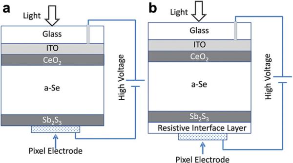
Two different types of solid-state a-Se detector structures were prepared based on the HARP target used in a vacuum tube device: standard pixelated HARP structure (Type 1), in which 0.8 mm2 gold contacts have been deposited by sputtering directly on a-Se blocking layer (Fig. 1 a), and modified pixelated HARP photosensor (Type 2) in which a 1 μm thick RIL (using CA) was spin-coated (in clean room environment, under controlled deposition parameters like: accelerating, decelerating, rotation speed and temperature) prior to the deposition of a 0.8 mm2 gold contact (Fig. 1 b). The HARP structure consists of a 15 μm a-Se photoconductor, sandwiched between 10 nm thick CeO2 layer and 0.5 μm thick Sb2S3 layer (hole and electron blocking layers, respectively), deposited on an ITO-coated glass substrate (Fig. 1). The details of this structure design can be found in Refs. [5–7].
Fig. 1.
Schematic picture of a-Se structures under investigation: (a) a-Se pixelated HARP blocking structure; (b) a-Se pixelated HARP blocking structure with Resistive interface layer between a-Se and metal electrode.
2.2. Time-of-flight measurement
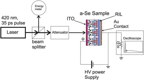
Time-Of-Flight (TOF) technique [17] was used to investigate transport and charge collection in both types of a-Se photosensors. For TOF measurements photosensors were exposed from the ITO side to a short (35 ps) laser pulses with the wavelength of 420 nm (which corresponds to the peak emission from scintillation crystals used in PET) and the current transients were monitored at various applied electric fields F by a 6 GHz bandwidth digital oscilloscope (Fig. 2). In both types of a-Se photosensors the electric field across the a-Se layer was created by connecting a positive voltage supply to an ITO layer (Fig. 2). The range of applied electric field was 10–104 V/μm for Type 2 samples (with RIL) and 10–80 V/μm for Type 1 (w/out RIL). Fields applied to Type 1 samples were restricted to prevent the dielectric breakdown which was found to occur above 80 V/μm after a few seconds of operation. It should be noted that in a signal mode (i.e. when a photosensor is exposed to a very short light pulse) the presence of CA layer does not affect either the photocurrent or charge collection from the structure since the capacitance of CA layer is 30 times larger than that of a-Se layer.
Fig. 2.
Schematic representation of Time-Of-Flight experimental apparatus which is used for measurement of electron-hole pair generation in a-Se.
Due to the short absorption depth in a-Se at 420 nm, electron-hole pairs (EHP) are generated close to the ITO/a-Se interface. The photogenerated holes traverse a distance equal d whereas the photogenerated electrons travel only a very short distance to the ITO contact. The duration of the laser pulse was negligible in comparison with both the RC constant of a-Se layer and the transit time for holes under all experimental conditions. All measurements were made at room temperature. Current transients for holes allowed us to calculate hole transient time and mobility while the integration of transient photocurrents allowed us to obtain the kinetics of charge collection at different electric field regimes. This in turn permits to derive the ratio between total collected electrons and holes (ne/nh). The importance of this ratio is that it allows an accurate calculation of the avalanche gain at different fields.
3. Results
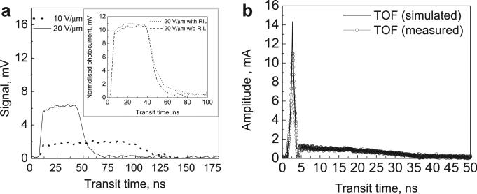
Our results confirm that modified HARP structures with 1 μm thick CA layer as a RIL withstand a very high electric field (about 100 V/μm) without dielectric breakdown: high electric field could be cycled up and down many times with no change in properties. In contrast, without CA coating standard HARP photosensor with metal electrodes undergoes breakdown after few seconds of operation if biased at about 80 V/μm or higher. However, the presence of a foreign layer like RIL may in principle enhance charge trapping at a-Se/RIL interface deteriorating transient performance. TOF measurements were performed to clarify this issue. Fig. 3 (a, b) show photocurrent pulses at electric fields below and above avalanche multiplication threshold FAV, respectively.
Fig. 3.
(a) Hole transit time curves for modified a-Se HARP blocking structure (with RIL) at different field intensities in the non-avalanche region. Insert shows comparison between structure, with and without RIL. (b) TOF signal from a-Se HARP blocking structure with RIL in avalanche regime for electric field 100 V/μm.
As it is seen from Fig. 3 (a) the hole transient profile for Type 2 structures at F < FAV has a quasi-rectangular shape with well-defined knee which corresponds to the hole transit time th (photogenerated electrons do not contribute significantly to the photocurrent since they are captured rapidly upon photogeneration travelling a very small distance to the positive electrode). The insert in Fig. 3 (a) compares hole transients for Type 1 and 2 samples at the same bias of 300 V. The similarity in photocurrent indicates that both, transport properties and th are unaffected by the presence of RIL.
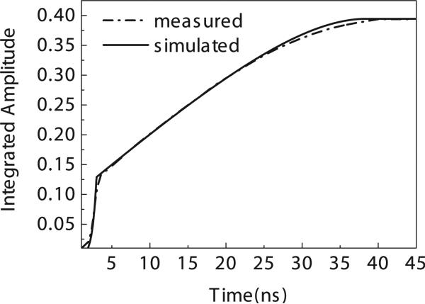
The shape of the photocurrent in avalanche regime (F>FAV) is different from that in non-avalanche regime (Fig. 3(b)) and exhibits rapid increase due to the motion of avalanching hole followed by comparatively long tail due to the slow motion of secondary non-avalanching electrons which are created in the trail of avalanching holes. Integrated TOF curve on Fig. 4 shows charge collection curve at a selected field F = 100 V/μm (above the avalanche multiplication threshold). As it is evident from Fig. 4, the fast leading edge due to the collection of avalanching holes is followed by a comparatively slow rise due to the collection of much slower non-avalanching electrons.
Fig. 4.
Variation with time, of the integrated TOF signal at 100 V/μm.
The slope change in integrated curves allows us to define the hole transit time th while saturation of the total collected charge allows us to define electron transit time te in avalanche regime. From the measurements of th and te we derive drift mobilities for holes and electrons, μh and μe, respectively:
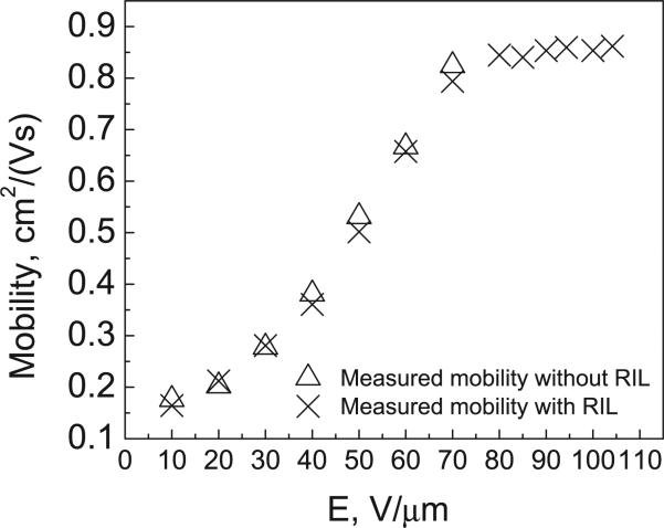
Field dependence of hole drift mobility μh is shown in Fig. 5. As it can be seen from Fig. 5, hole mobilities at F < FAV are similar for both types of photosensors. Electron drift mobility μe was found to be almost field independent in the range of F under consideration and with a magnitude of 0.06 cm2/(Vs). Electron and hole mobilities derived from the analysis of our TOF measurements were compared with the corresponding findings for a-Se insulating structures which have been used by Juska and Arlauskas [3,18] to demonstrate avalanche multiplication phenomenon in a-Se. In their work a-Se monolayer was confined between two insulating layers permitting application of high electric field needed for avalanche without charge injection. Although insulating structures cannot be used as practical photosensors (as no exit of mobile charge is possible because of insulating layers) they serve as a baseline for our research.
Fig. 5.
The variation of hole mobility with applied field.
4. Discussion
Comparative analysis of charge transport in standard and modified HARP structures clearly show that there is no noticeable trapping at a-Se/CA boundary. At sub-avalanche regime, transport in Type 2 structure remains non-dispersive like in “virgin” (Type 1) HARP structures and in a-Se insulating structures [3]: in both Type 1 and Type 2 structures a constant current and well-defined transit time (insert to Fig. 3) have been observed. Furthermore, as it is seen from Fig. 5, hole mobilities in non-avalanche regime are identical for Type 1 and Type 2 structures. The field dependence of hole drift mobilities for F < FAV is similar to that observed for a-Se insulating structures: mobility increases rapidly with field and reaches the value ~0.8 cm2/Vs at the threshold of avalanche multiplication FAV [3]. Because of breakdown it was impossible to measure hole mobility in avalanche regime (F>FAV) for Type I sample. These measurements were done for Type II sample with RIL only. As it is seen from Fig. 5 at F ≥ FAV holes propagate with mobility which nearly does not depend on field. This is a “prototype” behaviour for hole mobility in a-Se where hole transport is controlled by trapping into localised states within the band tails. An increase in electric field results in the heating of holes and the transition to field independent microscopic mobility at the threshold of avalanche multiplication [18]. This transition agrees well with the modified Lucky Drift (LD) model recently suggested for the explanation of avalanche multiplication in amorphous solids [1]. Indeed, the modified LD model requires carrier to move without trapping as a prerequisite for impact ionization. The microscopic mobility μ0 for a-Se insulating structures was found to be 0.8 cm2/Vs [18] in excellent agreement with our results.
Electron drift mobilities were calculated for Type 2 structures for F>FAV and were found to be field independent with a magnitude of 0.06 cm2/(Vs) in a good agreement with results obtained for a-Se insulating structures [18].
Thus obtained mobilities have been used as input parameters for the simulation of theoretical photoresponse in avalanche regime. For this simulation an analytical expression for the avalanche current was derived based on the following assumptions: (1) only holes can avalanche at applied fields; electrons do not avalanche with mobilities more than an order of magnitude smaller than those for holes (0.06 cm2/Vs for electrons vs 0.8 cm2/Vs for holes) (2) avalanche occurs uniformly through the a-Se thickness with multiplication coefficient which depends exponentially on traversed distance x [11]; (3) the photocurrent is not space-charge perturbed (the amount of charge in the bulk does not significantly affect the field). Under these assumptions and using Ramo's theorem, the induced current due to drift of avalanching holes is
| (1) |
where e is the elementary charge.
The induced current due to the drift of non-avalanching secondary electrons is:
| (2) |
where te = d/μeF is the electron transit time, γp is the hole impact ionization coefficient, n0, p0 is the number of electrons and holes respectively injected by a pulse of light at the positive contact.
| (3) |
Eq. (3) has been used to simulate total photocurrent at avalanche regime using experimentally measured field dependencies of μh,μe and gp [11]. p0 and n0 have been taken as free parameters to obtain the best possible fit to experimentally measured current transients. Good agreement of calculated and experimental results isseen from Fig. 3 (b) showing the validity of our analytical approach.
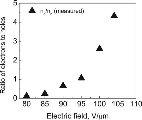
Charge collection curves (Fig. 4) have been used to analyse the relative contribution to photocurrent of secondary electrons and holes created as a result of impact ionization. The field dependence of electron-to-hole ratio (ne/nh) calculated from charge collection curves is shown in Fig. 6. As it is seen from Fig. 6 at comparatively low fields (below ~95 V/μm) (ne/nh) < 1 meaning that holes contribute more to the externally measured charge than electrons. At higher fields (ne/nh) exceeds unity and electrons become the major contributors to the measured signal. The inequality occurs because the charge induced in the external circuit depends on the distance traveled by a carrier as a fraction of detector thickness (Fig. 7). This distance in turn depends on the depth within the detector at which the impact ionization occurs and the charge is generated. At gAV = 1 electrons are created very close to the positive electrode and are rapidly collected with negligible contribution to the measured TOF signal, while the holes travel practically the entire depth of the detector, towards the negative electrode, creating the TOF signal. Therefore for F ≤ FAV the contribution to the signal is almost entirely due to holes. On the other hand, at F > FAV, as the drifting holes cause impact ionization, electrons are created at larger distances from the positive electrode and they start to contribute to the TOF signal traveling towards the positive electrode. At a gain of 5.2, the electrons and holes equally contribute to the TOF signal. As multiplication coefficient gAV depends exponentially on distance traveled, according to this equation:
| (4) |
Fig. 6.
The variation of the ratio of electrons to holes contributing to the TOF signal with applied field.
Fig. 7.
Distribution of hole concentration in bulk of a-Se in high electric field where impact ionization of holes occurs. Solid line and dash line corresponds to the motion of holes and electrons respectively.
The higher the gain, more secondary electron-hole pairs are created close to the negative surface of a-Se. Consequently holes are rapidly collected at the negative pole with minor contribution to the TOF signal while electrons traverse the entire thickness of the layer back to the positive electrode with major contribution to the measured signal (Fig. 7). At 104 V/μm, the electrons to holes ratio reaches a maximum of 4.6 (Fig. 6).
The experimentally measured electron-to-hole ratio provides a convenient method to measure the avalanche gain gAV independently of any other parameter. This is possible in a-Se because of the significant difference in the mobilities of holes and electrons as shown above. To derive (ne/nh) dependence on gAV we describe the number of carriers, dn, generated in the layer bounded by x and x + dx by impact ionization by the following differential equation:
| (5) |
With the solution:
| (6) |
The holes travel forward for a distance (d–x) therefore generating a signal:
| (7) |
Similarly, electrons while traveling in opposite direction for a distance x generate a signal:
| (8) |
The sum of these two signals gives dn. Combining these equations we obtain:
| (9) |
| (10) |
Which are solved to yield:
| (11) |
| (12) |
| (13) |
The ratio ne/nh is then obtained as:
| (14) |
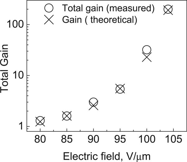
Equation (14) allows us to calculate numerically gAV for known (ne/nh). The results are plotted in Fig. 8 (open circles). The gain of 200 is achieved at F = 104 V/μm. Further increase in electric field will result in triggering of electrons impact ionization and self-sustaining avalanche breakdown (Geiger) process [3,12]. For comparison we have calculated gAV with the Eq. (4) using previously measured field dependence of hole impact ionization coefficient [1] (Fig. 8, crosses). The excellent agreement between measured and calculated results is obvious from Fig. 8 proving the validity of our approach.
Fig. 8.
The variation of the total gain of holes with the applied field.
5. Conclusion
The results on transport properties of the modified a-Se HARP structure show that a Resistive Interface Layer (RIL) made of Cellulose Acetate (CA) is a practical solution for the implementation of metal electrodes to avalanche a-Se photosensors: it improves stability against dielectric breakdown while hole transport is nondispersive and the mobility is not compromised as often happens if a “foreign” layer is introduced into the structure. A gain of 200 at 104 V/μm has been demonstrated for the modified HARP structure with 15 μm thick a-Se layer, which is the maximum theoretical gain for this thickness [4,12]. Moreover, the shape of the photocurrent and the field dependence of the hole mobility in the modified HARP are shown to be identical to those obtained in “prototype” insulating a-Se samples by Juska and Arlauskas [3,18], who discovered avalanche multiplication in a-Se in the early 80's using metal/polymer/a-Se/polymer/metal sandwich structures. In contrast to the insulating a-Se structure which cannot be used as a practical avalanche photosensor as no exit of mobile carriers were allowed, the presented modified a-Se HARP structure is the first practical approach to the a-Se avalanche photosensor with metal electrodes. We believe that the modified HARP represents the future of a-Se photodetectors in radiation medical imaging in both direct conversion detectors for low energy applications (like protein crystallography) and in indirect conversion detectors (like PET).
Acknowledgement
Financial support from Ontario Research Fund (gs1) - Research Excellence program and NIH (EB002655) is gratefully acknowledged.
References
- 1.Reznik A, Baranovskii SD, Rubel O, Juska G, Kasap S, Ohkawa Y, Tanioka K, Rowlands JA. J. Appl. Phys. 2007;102:053711. [Google Scholar]
- 2.Jandieri K, Rubel O, Baranovskii SD, Reznik A, Rowlands JA, Kasap SO. J. Mater. Sci. Mater. Electron. 2009;20:S221. [Google Scholar]
- 3.Juska G, Arlauskas K. Phys. Stat. Sol. (a) 1983;77:387. [Google Scholar]
- 4.Reznik A, Baranovskii SD, Rubel O, Jandieri K, Rowlands JA. Phys. Stat. Sol. (c) 2008;5:790. [Google Scholar]
- 5.Tanioka K, Yamazaki J, Shidara K, Taketoshi K, Kawamura T, Ishioka S, Takasaki Y. IEEE Electron Device Lett. 1987;8:392. [Google Scholar]
- 6.Yamazaki J, Kubota M, Maruyama H, Tanioka K, Shidara K, Hirai T, Tsuji K, Takasaki Y, Yamamoto M. Television Gakkai-shi. 1992;46:1189. [Google Scholar]
- 7.Ohkawa Y, Miyakawa K, Matsubara T, Kikuchi K, Suzuki S, Kubota M, Egami N, Kobayashi A. Phys. Status Solidi C. 2009;6(S1):S224–S226. [Google Scholar]
- 8.Kasap S, Frey JB, Belev G, Tousignant O, Mani H, Laperriere L, Reznik A, Rowlands JA. Phys. Status Solidi B. 2009;246:1794–1805. [Google Scholar]
- 9.Maruyama E. Jpn. J. Appl. Phys. 1982;21(2):213. [Google Scholar]
- 10.Reznik A, Lui BJM, Ohkawa Y, Matsubara T, Miyakawa K, Kubota M, Tanioka K, Kawai T, Zhao W, Rowlands JA. Nucl. Instrum. Methods Phys. Res. A. 2006;567:93. [Google Scholar]
- 11.Reznik A, Baranovskii SD, Rubel O, Jandieri K, Kasap SO, Ohkawa Y, Kubota M, Tanioka K, Rowlands JA. J. Non-Crystalline Solids. 2008;354:2691. [Google Scholar]
- 12.Reznik A, Zhao W, Ohkawa Y, Tanioka K, Rowlands JA. J. Mater. Sci. Mater. Electron. 2009;20:S63–S67. [Google Scholar]
- 13.Ohshima T, Tsuji K, Sameshima K, Hirai T, Shidara K, Teketoshi K. Jap. J. Appl. Phys. 1991;30:L1071. [Google Scholar]
- 14.Wronski M. Thesis. 2009. Development of a flat panel detector with avalanche gain for interventional radiology. [Google Scholar]
- 15.Wronski M, Zhao W, Reznik A, Tanioka K, Decscenzo G, Rowlands JA. A solid state amorphous selenium avalanche technology for low photon flux imaging applications. Med. Phys. 2010;37:9. doi: 10.1118/1.3483096. [DOI] [PMC free article] [PubMed] [Google Scholar]
- 16.Curry TS, Dowdey JE, Murry RC. Christensen's Physics of Diagnostic Radiology. fourth ed. Lipnicott Williams & Wilkins; 1990. [Google Scholar]
- 17.Street RA. In: Hydrogenated Amorphous Silicon. Cahn RW, Davis EA, Ward IM, editors. Cambridge University Press; 1991. pp. 62–95. Chapter 3. [Google Scholar]
- 18.Juska G, Arlauskas K. Impact ionization and mobilities of charge carriers at high electric fields in amorphous selenium. Phys. Stat. Sol (a) 1980;59:389–393. [Google Scholar]


