Abstract
The ability to manipulate quantum states of light by integrated devices may open new perspectives both for fundamental tests of quantum mechanics and for novel technological applications. However, the technology for handling polarization-encoded qubits, the most commonly adopted approach, is still missing in quantum optical circuits. Here we demonstrate the first integrated photonic controlled-NOT (CNOT) gate for polarization-encoded qubits. This result has been enabled by the integration, based on femtosecond laser waveguide writing, of partially polarizing beam splitters on a glass chip. We characterize the logical truth table of the quantum gate demonstrating its high fidelity to the expected one. In addition, we show the ability of this gate to transform separable states into entangled ones and vice versa. Finally, the full accessibility of our device is exploited to carry out a complete characterization of the CNOT gate through a quantum process tomography.
 As quantum information processing continues to develop apace, the need for integrated photonic devices becomes ever greater for both fundamental measurements and technological applications. To this end, Crespi et al. demonstrate a high-fidelity photonic controlled-NOT gate on a glass chip.
Incorporating the laws of quantum mechanics in data storage, processing and transmission may unleash new possibilities for information processing, ranging from quantum communication to quantum sensing, metrology, simulation and computing1,2,3,4. In the last few years photonic quantum technologies have been adopted as a promising experimental platform for quantum information science3. The realization of complex optical schemes consisting of many elements requires the introduction of waveguide technology to achieve desired scalability, stability and miniaturization of the device. Recently, silica waveguide circuits on silicon chips have been employed in quantum applications to realize stable interferometers for two-qubit entangling gates5. Such approach with qubits encoded into two photon optical paths, representing the logical basis {|0〉,|1〉}, yielded the first demonstration of an integrated linear optical controlled-NOT (CNOT) gate. In addition, quantum walk on a chip6,7 and enhanced quantum sensitivity in phase-controlled interferometers have been demonstrated with the same technology8,9,10,11. However, many quantum information processes and sources of entangled photon states are based on the polarization degree of freedom4,12, which allows one to implement quantum operations without the need of path duplication and thus with the simplest and most compact circuit layout. Up to now, integrated devices able to efficiently guide and manipulate polarization-encoded photonic qubits are still lacking13.
Femtosecond laser waveguide writing has been emerging as a powerful tool in the rapidly advancing field of quantum photonics14. This technique, which was first introduced by Davis et al. in 1996 (ref. 15), exploits nonlinear absorption of focused femtosecond pulses to induce permanent and localized refractive index increase in transparent materials. Waveguides are directly fabricated in the bulk of the substrate by translation of the sample at constant velocity with respect to the laser beam, along the desired path. This maskless and single-step technique allows fast and cost-effective prototyping of new devices, potentially exploiting also three-dimensional geometries impossible to obtain with conventional lithography. Several devices, from simple Y-splitters16 to increasingly complex ones17,18,19, have been demonstrated with applications ranging from telecommunications to integrated biosensing20,21. This technique is capable of producing high-quality waveguides with low birefringence, which are indeed suited for the propagation of polarization-encoded qubits, as we recently reported in refs 22,23, where a polarization-insensitive directional coupler has been demonstrated.
Here we report on the first integrated photonic CNOT gate for polarization-encoded qubits and on the complete characterization of its quantum behaviour. The demonstration of this quantum gate has been made possible by the fabrication in a glass chip of integrated devices acting as partially polarizing beam splitters (PPBSs). Precisely, we show that femtosecond laser writing enables direct inscription of directional couplers with fine and independent control on the splitting ratio for the horizontal (H) and vertical (V) polarizations.
Results
Directional couplers as partially polarizing beam splitters
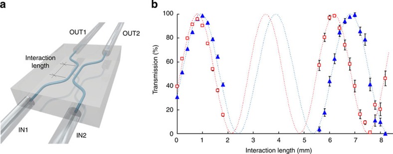
Directional couplers are the integrated optical analogue of bulk beam splitters (BSs) and are thus fundamental building blocks of quantum optical circuits. In these devices (see the schematic representation in Fig. 1a) two distinct waveguides are brought close together for a certain propagation length, called interaction length, so that the two propagating modes become coupled through evanescent field overlap. In analogy to bulk BSs, reflectivity and transmissivity ratios of the directional coupler can be conveniently defined: when light is launched into port IN1 (Fig. 1a), R=POUT1/(POUT1+POUT2) and T=1−R=POUT2/(POUT1+POUT2), respectively (P indicates the optical power); the symmetry of the device guarantees that the same relations hold when light is launched into port IN2, by simply inverting the two indices. Optical power transfer from one waveguide to the other follows a sinusoidal law with the interaction length, whose oscillation period (beating period) depends upon the coupling coefficient of the two guided modes according to coupled mode theory24. If some waveguide birefringence is present, the coupling coefficient, and hence the beating period, can be different for the two polarizations (Fig. 1b). With high birefringence waveguides, this aspect has been exploited to implement polarizing beam splitters for telecom applications25.
Figure 1. Partially polarizing directional couplers.
(a) Schematic representation of a waveguide directional coupler; IN1 and IN2 are the input ports, whereas OUT1 and OUT2 are the output ports of the device. (b) H (squares) and V (triangles) polarization transmissions of directional couplers with different interaction lengths, based on slightly birefringent waveguides. First, the 0–2 mm interaction length range was investigated to evaluate the beating length difference between the two polarizations; the interval of interest to obtain the required PPDCs was estimated to be in the 5.6–8.2 mm range, which was consequently explored. Transmission for 0 mm interaction length is non-zero, because some coupling already occurs in the curved portions of the approaching/departing waveguides. Error bars indicate fabrication reproducibility.
However, high birefringence waveguides are not suitable for the propagation of polarization-encoded qubits as they would cause decoherence between the photons typically generated by parametric down conversion, which are characterized by a large bandwidth Δλ>1 nm. The optimal waveguides for a polarization-based quantum gate would therefore need to find the best compromise on the birefringence value, which should be low enough to preserve the coherence between photons, and high enough to enable polarization-dependent processing. Such compromise is found in femtosecond laser written waveguides in a borosilicate glass. In fact, thanks to their low birefringence, these waveguides allow to propagate polarization-encoded qubits without any perturbation and also to achieve practically polarization-insensitive devices, as demonstrated in refs 22,23. However, in this work we demonstrate that the same waveguides are also capable of performing polarization-based processing of the qubits. In fact, if sufficiently long interaction lengths, covering a few beating periods, are implemented in directional couplers, it is possible to strongly enhance the difference in the polarization behaviour of the device. This approach, as shown in Figure 1b, allows to finely tailor the splitting ratios for the two polarizations and enables us to realize integrated PPBSs for the first time.
Integrated quantum gates for polarization-encoded qubits
We will now demonstrate how this technology can be exploited to realize quantum optical gates. In the polarization-encoding approach, a generic qubit α|0〉+β+1〉 is implemented by a coherent superposition of H and V polarization states, α|H〉+β|V〉, of single photons. To achieve universal quantum computation, single qubit transformations together with a two-qubit gate are sufficient26. One-qubit logic gates are straightforwardly implemented by using birefringent waveplates. The most commonly exploited two-qubit gate is the CNOT that flips the target qubit (T) depending on the state of the control one (C). The CNOT action is described by a unitary transformation acting on a generic superposition of two qubit quantum states. In the computational basis {|00〉,|01〉,|10〉,|11〉} for the systems C and T, the matrix associated to the CNOT is:
 |
1 |
A striking feature of this gate is given by the ability to entangle and disentangle qubits. Precisely, the input states |±〉C|0〉T and |±〉C|1〉T, where  , evolve into the following output states
  and
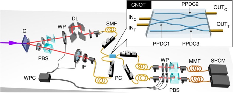
and  , which are the so-called Bell states. Photonic two-qubit gates need an interaction between the two photons that carry the information, and this would suggest that a strong optical nonlinearity is required. However, it was demonstrated that scalable quantum computing is possible by using only linear optical circuits, mainly consisting of beam splitters28. The most simple scheme to implement the polarization CNOT exploits three PPBSs with suitable polarization-dependent transmissivites29,30. The two-photon interaction occurs by a Hong–Ou–Mandel effect31 in a single PPBS, whereas the other two PPBSs operate as compensators. Up to now such a scheme has been experimentally implemented only using bulk optics32,33,34,35 or fibre couplers36. The integrated CNOT gate is achieved by the optical scheme given in the inset of Figure 2: it consists of a first partially polarizing directional coupler (PPDC1), with transmissivities TH(1)=0 and
  for horizontal and vertical polarization, respectively, where target and control qubits interfere, followed by two other directional couplers (PPDC2 and PPDC3), with
  and
and  , where the horizontal and vertical polarization contributions are balanced. In this scheme, the following correspondence between logical qubits and physical states holds: |0〉C≡|V〉C, |1〉C≡|H〉C, |0〉T≡|A〉T, |1〉T≡|D〉T where
  and
and  . The CNOT operation succeeds with probability
  .
.
Figure 2. Experimental setup.
Sketch of the experimental setup that can be conceptually divided into three parts. The first part is the source: photon pairs at wavelength λ=806 nm are generated via spontaneous parametric down conversion in a 1.5 mm β-barium borate crystal (C) cut for type-II non-collinear phase matching, pumped by a CW diode laser with power P=50 mW (ref. 27). Photon polarization states are prepared by using polarizing beam splitters (PBSs) and waveplates (WPs). A delay line (DL) is inserted to control the temporal superposition of the photons, which are then coupled to single mode fibres (SMFs) and injected into the integrated CNOT gate. Interference filters (IFs) determine the photon bandwidth Δλ=6 nm. The second part shows the integrated CNOT for polarization-encoded qubits (see inset) realized by ultrafast laser writing technique. The final part represents the analysis apparatus: the polarization state of qubits emerging from the chip is analyzed by standard analysis setups (WP+PBS). Photons are then delivered to single photon counting modules (SPCM) through multimode fibres (MMFs) and coincidences between the two channels are measured. Polarization controllers (PCs) are used before and after the CNOT device to compensate polarization rotations induced by the fibres. A waveplate controller (WPC) drives the motorized waveplates to automatize the measurements.
The PPDCs have been fabricated by the femtosecond laser waveguide writing technique above described. To calibrate the fabrication parameters, several directional couplers have been produced with different interaction lengths ranging from 0 mm to 2 mm and from 5.6 mm to 8.2 mm (see Fig. 1). The distance between the two waveguides in the interaction region was kept constant at 7 μm. It can be observed that for an interaction length L1≃7.4 mm a device with TH=0 and  is obtained, fulfilling the requirements for PPDC1, whereas a length L2≃7 mm provides
  and TV=1 and can be adopted for PPDC2 and PPDC3. Several CNOTs have been fabricated according to the schematic of Figure 2 (inset) with slightly different interaction lengths around the values of L1 and L2 to take into account possible fabrication imperfections. The footprint of each integrated CNOT is 500 μm×3 cm. After characterization with a classical laser source, the devices providing the best estimated performance have been selected. The device used in the experiments has the following parameters:
 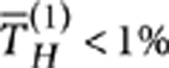 ,
,  ,
,  ,
,  ,
,  , and
, and  . To improve the robustness and stability of the device, single-mode fibre arrays have been permanently bonded to the input and output ports.
Quantum measurements
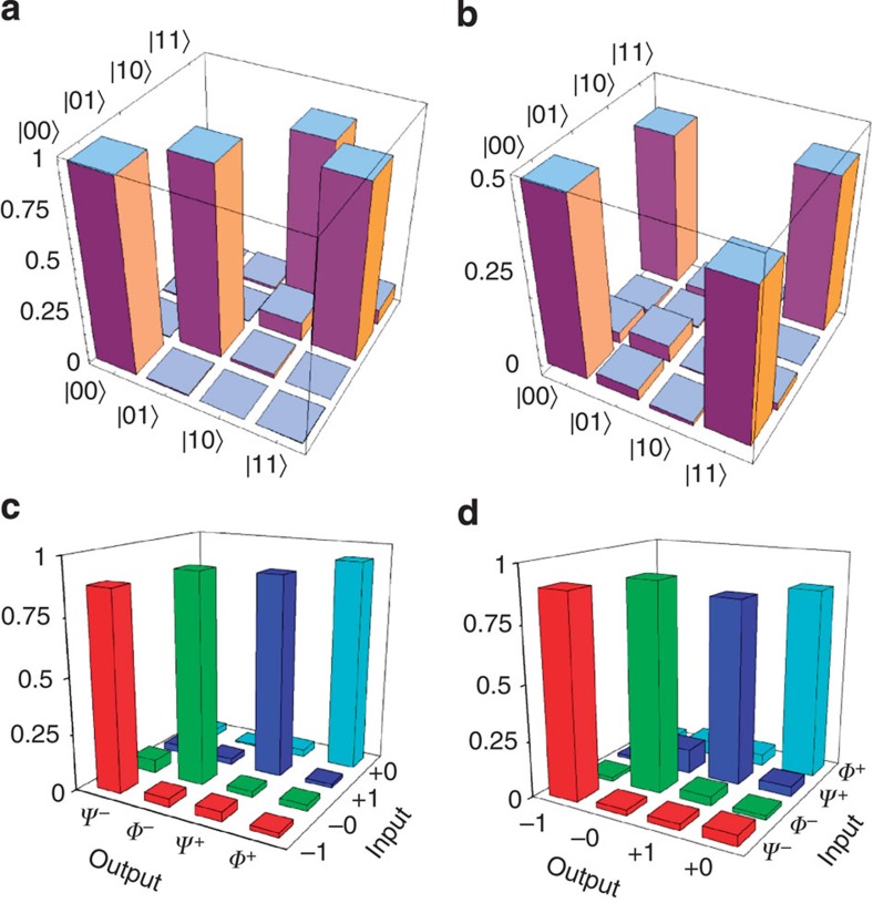
As a first quantum experiment we determined the truth table of the device operated as a CNOT gate. On this purpose we used the experimental setup represented in Figure 2. Temporal superposition of photon wavepackets in PPDC1 was obtained by acting on the delay line. Then we injected into the chip the four computational basis states |0〉C|0〉T, |0〉C|1〉T, |1〉C|0〉T and |1〉C|1〉T and measured the probability of detecting each of them at the output. The obtained truth table is reported in Figure 3a. The average measured fidelity of the logical basis32 has been calculated as F=0.940±0.004. We can compare this value with the expected fidelity of the device  , estimated by taking into account the measured transmissivities of the PPDCs. We attribute the discrepancy between the experimental and expected fidelities mainly to a partial distinguishability of photon wavepackets and non-perfect compensation of the rotation of the polarization in the single-mode optical fibres.
Figure 3. Truth table and entanglement generation.
(a) Measured truth table. (b) Experimental tomographic reconstruction of the Bell state |Φ+〉 obtained by injecting the separable state |+0〉 in the CNOT. (c) Measured probabilities of the output Bell states corresponding to the different input separable states. (d) Measured probabilities of the output separable states corresponding to the different input Bell states.
As already mentioned, the CNOT can also be exploited as an entangling gate. We experimentally verified this behaviour by injecting into the device the states {|±〉C|0〉T,|±C|1〉T} and measuring a set of observables to obtain a tomographic reconstruction of the density matrices of the output states. As expected the action of the CNOT converts the separable states into the maximally entangled Bell states. We report in Figure 3b one of the reconstructed density matrices and in Figure 3c the probabilities to generate the different Bell states. The fidelities of the output density matrices compared with those of the corresponding Bell states are 


 with average value
  . We also checked that the CNOT gate can be adopted to discriminate the four Bell states. Indeed, the four entangled states
  are transformed into four orthogonal separable states, which can be easily discriminated, as shown in Figure 3d. The discrimination probability is 0.877±0.007, slightly lower than the previous fidelities due to imperfections in the entanglement source.
To provide a full characterization of the quantum device we carried out a quantum process tomography37, first experimentally demonstrated for a CNOT gate in ref. 38. This requires preparing the photons in a complete set of input basis states, and characterizing the output. A generic quantum process  acting on a two-qubit density matrix ρ, can be expressed as
  where the operators Γm are defined as tensor products of Pauli matrices {Γm≡σi
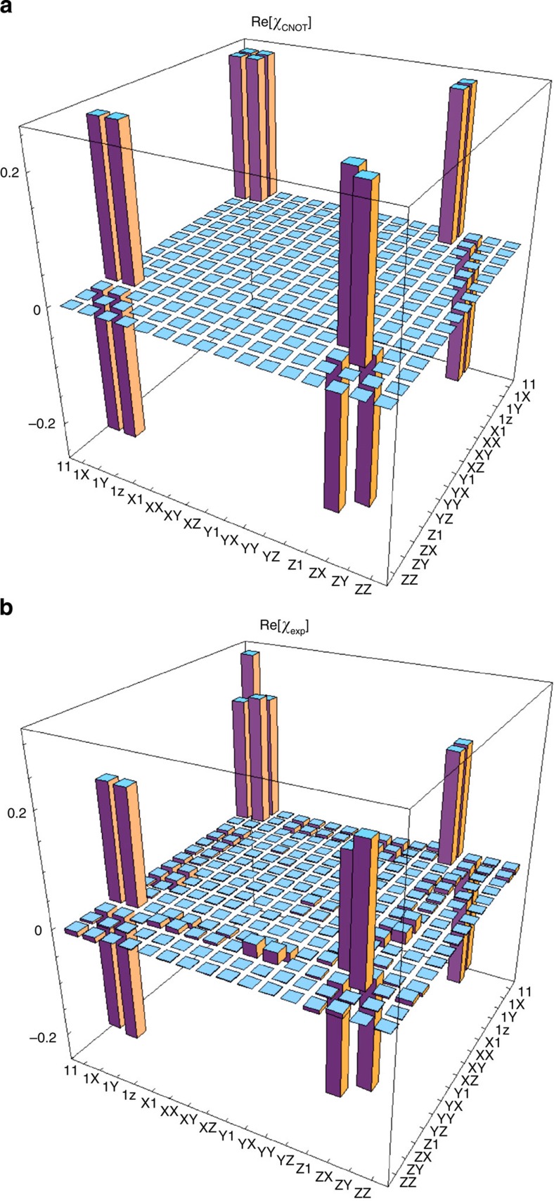
 σj}, i, j=0, ..., 3, m=0, ..., 15. The matrix χmn contains all the information of the process. We reconstructed the 16×16 matrix χexp shown in Figure 4. The process fidelity39 (see Methods) with the ideal CNOT gate was measured as exp=0.906±0.003.
Figure 4. Process matrix measurement.
(a) Ideal χCNOT and (b) experimental χexp matrices (real part) obtained from the quantum process tomography of the CNOT gate. Imaginary part of χexp is negligible. X, Y and Z correspond to Pauli matrices σ1, σ2 and σ3, respectively.
Discussion
We reported on the integration of partially polarizing beam splitters on a glass chip, enabling the demonstration of the first integrated photonic CNOT gate based on polarization encoding. From the fabrication point of view this work shows the capability of femtosecond laser microfabrication to produce also polarization-sensitive waveguide devices, thus further enriching the portfolio of applications that can be addressed by this simple and flexible fabrication technique. It is important to note that the polarization sensitivity/insensitivity of the directional coupler can be selected by acting on geometrical parameters and not on physical properties of the waveguides22,23. This enables simple and flexible designs of complex integrated quantum devices, where polarization-sensitive and polarization-insensitive processing can be easily cascaded. This work represents a major step towards the development of integrated photonic technology, which could provide a viable solution for quantum information processing and paves the way to the integration of a wealth of polarization-based quantum algorithms. Future research will be devoted to the on-chip implementation of both preoriented and tunable waveplates to integrate also one-qubit gates. The present results open new perspectives towards joint integrated handling of hybrid quantum states based on different degrees of freedom of light40,41,42,43,44,45, such as polarization, path and orbital angular momentum. This would significantly improve the computational power of a quantum device.
The capability to process polarization-entangled photons could also benefit the quantum simulation field. As an example, exploiting the different statistics of singlet and triplet polarization-entangled states, it is possible to simulate how symmetric and antisymmetric particles travel through a quantum walk7,23, paving the way to advanced investigations on complexity physics phenomena.
Methods
Chip fabrication and characterization
Waveguides were micromachined in borosilicate glass substrate (Corning EAGLE2000, Corning Inc) using a commercial HighQLaser FemtoREGEN femtosecond laser, which provides 400 fs pulses at 960 kHz repetition rate. For the waveguide fabrication pulses with 240 nJ energy were focused 170 μm under the glass surface, using a 0.6 numerical aperture microscope objective whereas the sample was translated at a constant speed of 20 mm s−1 by high precision, three-axis air-bearing stages (Aerotech FiberGlide 3D, Aerotech Inc). The guided mode at 806 nm is slightly elliptical, measuring 8 μm×9 μm. Measured propagation losses are 0.8 dB cm−1 and coupling losses to single mode fibres about 1.3 dB per facet. Birefringence of these waveguides is on the order of B=7×10⁻⁵, as characterized in ref. 22. For the curved segments in the directional couplers composing the integrated CNOT a 30 mm bending radius was adopted, which gives <1 dB of additional bending losses on the whole device.
Quantum process tomography
The full characterization of a quantum device is provided by quantum process tomography37. Following the procedure adopted in ref. 39. we performed the quantum process tomography of our device and reconstructed the associated χ matrix. The experimental setup is the same one adopted in the previous measurements (see Fig. 2): we prepared 16 different input states and measured the projections of the output states on the set {|ij〉}, where i, j=H,V,D,A,R,L, that is, horizontal, vertical, diagonal, antidiagonal, righthanded and lefthanded polarization, using standard polarization analysis setups. The obtained χ matrix is reported in Figure 4. To evaluate the quality of the acquired data we calculated the process fidelity39 as
 |
2 |
where χCNOT is the process matrix of the ideal CNOT gate.
Author contributions
A.C., R.R., R.O., L.S., F.S., G.V., and P.M. conceived and designed the integrated CNOT gate for polarization qubits. A.C., R.R., R.O. fabricated the integrated CNOT chip and performed the characterization measurements in the classical regime. L.S., I.B., F.S., G.V., PM carried out the characterization measurements in the quantum regime. All authors discussed the results and participated in the manuscript preparation.
Additional information
How to cite this article: Crespi, A. et al. Integrated photonic quantum gates for polarization qubits. Nat. Commun. 2:566 doi: 10.1038/ncomms1570 (2011).
Acknowledgments
This work was supported by PRIN 2009: Circuiti Integrati per l'Informazione Quantistica, FIRB-Futuro in Ricerca HYTEQ, ERA-Net CHISTERA-QUASAR.
Footnotes
A.C., R.R., R.O., L.S., F.S., G.V. and P.M. are listed as inventors on an Italian patent pending application (PD2011A000140) entitled 'Porta logica in ottica integrata per qubit quantistici codificati in polarizzazione e relativo metodo di realizzazione ed utilizzo' dealing with the implementation of an integrated optics quantum logic gate according to the results presented in this paper
References
- Ladd T. D. et al. Quantum computers. Nature 464, 45–53 (2010). [DOI] [PubMed] [Google Scholar]
- O'Brien J. L., Furusawa A. & Vuckovic J. Photonic quantum technologies. Nat. Photon. 3, 687–695 (2009). [Google Scholar]
- Kok P. et al. Linear optical quantum computing with photonic qubits. Rev. Mod. Phys. 79, 135–174 (2007). [Google Scholar]
- Ursin R. et al. Entanglement-based quantum communication over 144 km. Nat. Phys. 3, 481–486 (2007). [Google Scholar]
- Politi A., Cryan M. J., Rarity J. G., Yu S. & O'Brien J. L. Silica-on-silicon waveguide quantum circuits. Science 320, 646–649 (2008). [DOI] [PubMed] [Google Scholar]
- Peruzzo A. et al. Quantum walks of correlated photons. Science 17, 1500–1503 (2010). [DOI] [PubMed] [Google Scholar]
- Matthews J. C. F. et al. Simulating quantum statistics with entangled photons: a continuous transition from bosons to fermions. Preprint at 〈http://arXiv.org/abs/1106.1166〉 (2011).
- Politi A., Matthews J. C. F. & O'Brien J. L. Shor's quantum factoring algorithm on a photonic chip. Science 325, 1221 (2009). [DOI] [PubMed] [Google Scholar]
- Smith B. J., Kundys D., Thomas-Peter N., Smith P. G. R. & Walmsley I. A. Phase-controlled integrated photonic quantum circuits. Opt. Express 17, 13516–13525 (2009). [DOI] [PubMed] [Google Scholar]
- Laing A. et al. High-fidelity operation of quantum photonic circuits. Appl. Phys. Lett. 97, 211109 (2010). [Google Scholar]
- Matthews J. C. F. et al. Manipulation of multiphoton entanglement in waveguide quantum circuits. Nat. Photon. 3, 346–350 (2009). [Google Scholar]
- Walther P. et al. Experimental one-way quantum computing. Nature 434, 169–176 (2005). [DOI] [PubMed] [Google Scholar]
- Politi A., Matthews J., Thompson M. & O'Brien J. Integrated quantum photonics. IEEE J. Sel. Top. Quant. Electron. 15, 1673–1684 (2009). [Google Scholar]
- Marshall G. D. et al. Laser written waveguide photonic quantum circuits. Opt. Express 17, 12546–12554 (2009). [DOI] [PubMed] [Google Scholar]
- Davis K. M. et al. Writing waveguides in glass with a femtosecond laser. Opt. Lett. 21, 1729–1731 (1996). [DOI] [PubMed] [Google Scholar]
- Homoelle D. et al. Infrared photosensitivity in silica glasses exposed to femtosecond laser pulses. Opt. Lett. 24, 1311–1313 (1999). [DOI] [PubMed] [Google Scholar]
- Gattass R. R. & Mazur E. Femtosecond laser micromachining in transparent materials. Nat. Photon. 2, 219–225 (2008). [Google Scholar]
- Della Valle G., Osellame R. & Laporta P. Micromachining of photonic devices by femtosecond laser pulses. J. Opt. A 11, 013001–013018 (2009). [Google Scholar]
- Osellame R. et al. Femtosecond writing of active optical waveguides with astigmatically shaped beams. J. Opt. Soc. Am. B 20, 1559–1567 (2003). [Google Scholar]
- Eaton S. M. et al. Telecom-band directional coupler written with femtosecond fiber laser. IEEE Phot. Technol. Lett. 18, 2174–2176 (2006). [Google Scholar]
- Osellame R. et al. Femtosecond laser microstructuring: an enabling tool for optofluidic lab-on-chips. Laser Phot. Rev. 5, 442–463 (2011). [Google Scholar]
- Sansoni L. et al. Polarization entangled state measurement on a chip. Phys. Rev. Lett. 105, 200503 (2010). [DOI] [PubMed] [Google Scholar]
- Sansoni L. et al. Two-particle bosonic-fermionic quantum walk via 3D integrated photonics. Preprint at 〈http://arXiv.org/abs/1106.5713〉 (2011). [DOI] [PubMed]
- Yariv A. Coupled-mode theory for guided-wave optics. IEEE J. Quantum Electron. 9, 919–933 (1973). [Google Scholar]
- Kiyat I., Aydinli A. & Dagli N. A compact silicon-on-insulator polarization splitter. IEEE Phot. Technol. Lett. 17, 100–102 (2005). [Google Scholar]
- Nielsen M. & Chuang I. Quantum Computation and Quantum Information, Cambridge University Press, 2000. [Google Scholar]
- Kwiat P. G. et al. New high-intensity source of polarization-entangled photon pairs. Phys. Rev. Lett. 75, 4337–4341 (1995). [DOI] [PubMed] [Google Scholar]
- Knill E., Laflamme R. & Milburn G. J. A scheme for efficient quantum computation with linear optics. Nature 409, 46–52 (2001). [DOI] [PubMed] [Google Scholar]
- Ralph T. C., Langford N. K., Bell T. B. & White A. G. Linear optical controlled-NOT gate in the coincidence basis. Phys. Rev. A 65, 062324 (2002). [Google Scholar]
- Hofmann H. F. & Takeuchi S. Quantum phase gate for photonic qubits using only beam splitters and postselection. Phys. Rev. A 66, 024308 (2002). [Google Scholar]
- Hong C. K., Ou Z. Y. & Mandel L. Measurement of subpicosecond time intervals between two photons by interference. Phys. Rev. Lett. 59, 2044 (1987). [DOI] [PubMed] [Google Scholar]
- Kiesel N., Schmid C., Weber U., Ursin R. & Weinfurter H. Linear optics controlled-phase gate made simple. Phys. Rev. Lett. 95, 210505 (2005). [DOI] [PubMed] [Google Scholar]
- Okamoto R., Hofmann H. F., Takeuchi S. & Sasaki K. Demonstration of an optical quantum controlled-NOT gate without path interference. Phys. Rev. Lett. 95, 210506 (2005). [DOI] [PubMed] [Google Scholar]
- Langford N. K. et al. Demonstration of a simple entangling optical gate and its use in bell-state analysis. Phys. Rev. Lett. 95, 210504 (2005). [DOI] [PubMed] [Google Scholar]
- O'Brien J. L. et al. Demonstration of an all-optical quantum controlled-NOT gate. Nature 426, 264–267 (2003). [DOI] [PubMed] [Google Scholar]
- Clark A. S. et al. All-optical-fiber polarization-based quantum logic gate. Phys. Rev. A 79, 030303(R) (2009). [Google Scholar]
- Chuang I. L. & Nielsen M. A. Prescription for experimental determination of the dynamics of a quantum black box. J. Mod. Opt. 44, 2455–2467 (1997). [Google Scholar]
- O'Brien J. L. et al. Quantum process tomography of a controlled- NOT gate. Phys. Rev. Lett. 93, 080502 (2004). [DOI] [PubMed] [Google Scholar]
- Bongioanni I., Sansoni L., Sciarrino F., Vallone G. & Mataloni P. Experimental quantum process tomography of non trace-preserving maps. Phys. Rev. A 82, 042307 (2010). [Google Scholar]
- Rossi A., Vallone G., Chiuri A., De Martini F. & Mataloni P. Multipath entanglement of two photons. Phys. Rev. Lett. 102, 153902 (2009). [DOI] [PubMed] [Google Scholar]
- Chiuri A. et al. Hyperentangled mixed phased Dicke states: optical design and detection. Phys. Rev. Lett. 105, 250501 (2010). [DOI] [PubMed] [Google Scholar]
- Gao W.- B. et al. Experimental realization of a controlled-NOT gate with four-photon six-qubit cluster states. Phys. Rev. Lett. 104, 020501 (2010). [DOI] [PubMed] [Google Scholar]
- Nagali E. et al. Optimal quantum cloning of orbital angular momentum photon qubits through Hong-Ou-Mandel coalescence. Nat. Photon. 3, 720–723 (2009). [Google Scholar]
- Nagali E. et al. Experimental optimal cloning of four-dimensional quantum states of photons. Phys. Rev. Lett. 105, 073602 (2010). [DOI] [PubMed] [Google Scholar]
- Barreiro J. T., Wei T.- C. & Kwiat P. G. Beating the channel capacity limit for linear photonic superdense coding. Nat. Phys. 4, 282–286 (2008). [Google Scholar]


