Abstract
High-resolution characterization methods play a key role in the development, analysis and optimization of nanoscale materials and devices. Because of the various material properties, only a combination of different characterization techniques provides a comprehensive understanding of complex functional materials. Here we introduce correlative infrared–electron nanoscopy, a novel method yielding transmission electron microscope and infrared near-field images of one and the same nanostructure. While transmission electron microscopy provides structural information up to the atomic level, infrared near-field imaging yields nanoscale maps of chemical composition and conductivity. We demonstrate the method's potential by studying the relation between conductivity and crystal structure in ZnO nanowire cross-sections. The combination of infrared conductivity maps and the local crystal structure reveals a radial free-carrier gradient, which inversely correlates to the density of extended crystalline defects. Our method opens new avenues for studying the local interplay between structure, conductivity and chemical composition in widely different material systems.
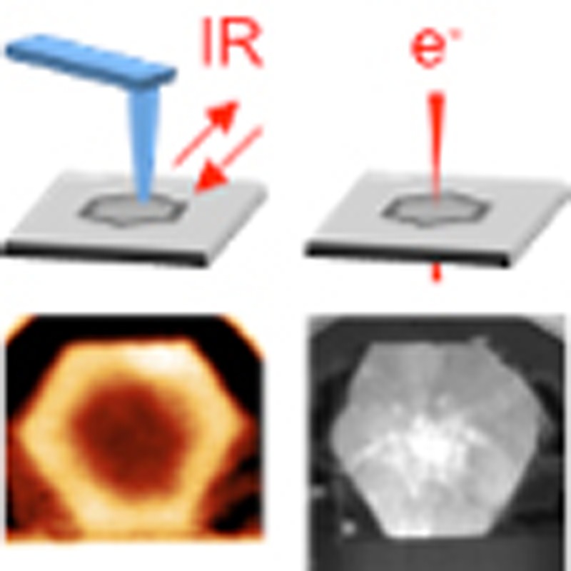 High-resolution characterisation techniques enable us to better understand the properties of nanoscale materials and devices. By combining electron microscopy and infrared nanoscopy, Stiegler et al. demonstrate a general approach to simultaneously probe the structural, chemical and electronic properties of a nanostructure.
Modern characterization of materials, devices or biological matter relies on a variety of high-resolution imaging techniques. Among the most important and well-established techniques is transmission electron microscopy (TEM)1 that allows for atomic-scale imaging of crystal structure and element distribution. Scanning probe microscopy2, on the other hand, provides surface topography and nanoscale information about mechanical, electrical and magnetic properties of the surface. For example, scanning tunnelling microscopy has been used successfully to study the structural and electrical properties among others of semiconductors3,4, and molecules5,6,7, however, it is limited to conductive samples. With the introduction of scattering-type scanning near-field optical microscopy (s-SNOM)8,9,10,11,12,13, even nanoscale infrared (IR) and terahertz imaging became possible. s-SNOM offers superior sensitivity to local chemical composition11,12,14,15,16 and conductivity9,13,17,18,19,20. It is typically based on an atomic force microscope (AFM). For probing local dielectric material properties, a metalized tip is used and illuminated by a focused laser beam. The metallic tip functions as an IR antenna converting the illuminating radiation into a highly localized and enhanced near-field at the tip apex13,21,22,23, similar to tip-enhanced Raman spectroscopy24,25,26,27. Owing to the optical near-field interaction between tip and sample, the light scattered by the tip is modified in both its amplitude and its phase, depending on the local dielectric properties of the sample28. Interferometric detection of the backscattered light thus yields nanoscale-resolved IR amplitude and phase images, revealing local structural properties29,30, material composition13,15,31,32,33,34, and the free-carrier concentration13,18,20,35.
Despite the intriguing capabilities of the individual characterization tools, it is the correlation of the physical and chemical properties obtained from different tools that will further a more comprehensive understanding of functional materials and complex devices. In materials research and biosciences, for example, correlative light–electron microscopy is a well-established and brilliant technique, providing unique insights into the relationship between the local structure and the function of semiconductor nanowires36,37,38,39,40,41 and biological matter42,43, respectively.Here, we introduce correlative IR–electron nanoscopy as a novel analytical tool for materials, bio- and nanosciences, allowing for the correlation of TEM images and nanoscale-resolved IR s-SNOM images of one and the same nanostructure or device. To demonstrate an application example of high technological relevance, we study the widely unexplored relation between local crystal structure and local conductivity in chemically grown ZnO nanowires. ZnO nanowire arrays have a high application potential in different technological domains, such as (opto-)electronics, solar cells and piezoelectrics, and have thus attracted great interest among emerging nanoscale materials44,45,46. This interest is owing to their unique combination of a peculiar morphology and (opto-)electronic properties. Apart from costly and technologically complicated vapour growth processes, arrays of ZnO single-crystal nanowires can be grown by low-temperature and cost-effective techniques such as hydrothermal47,48 and electrochemical49 deposition. Thus, low-temperature grown ZnO nanowires arrays are an ideal candidate for large-scale production, allowing the nanowire integration into devices using low-cost thin-film technology. These nanowires, however, exhibit a high density of defects, and it has been found experimentally that annealing can improve the performance of the nanowires in several applications. Although previous TEM studies have revealed a significant amount of defects in ZnO nanowires44,47,50, information about their influence on the local conductivity has been elusive. However, it is this information that is of utmost importance for the optimization of the growth process and thus the performance of the nanowires. Here, we study cross-sections of electrochemically grown ZnO nanowires by correlative IR–electron nanoscopy. We find a radial free-carrier profile in as-grown ZnO nanowires, which can be explained by a radial varying crystal quality caused by a combined core-shell growth of the nanowires.
Results
s-SNOM study of mechanically polished ZnO nanowire arrays
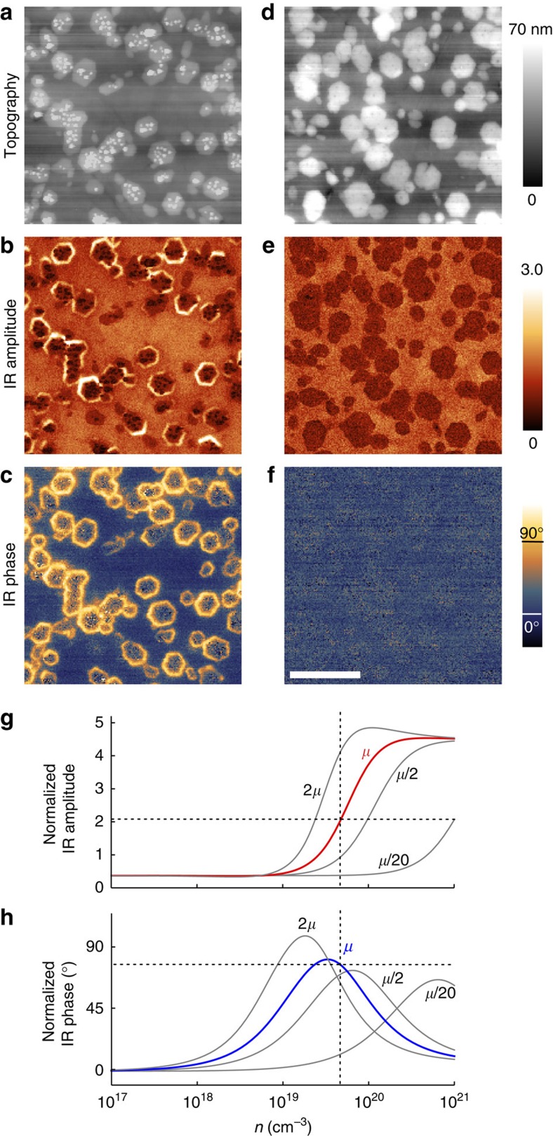
As a first step, we demonstrate the capability of s-SNOM for radial free-carrier profiling of semiconductor nanowires. To that end, we prepared mechanically polished cross-sections of electrochemically grown as-deposited (Fig. 1a–c) and annealed (Fig. 1d–f) ZnO nanowires (see Methods) embedded into a CuSCN matrix—a typical configuration in light-emitting diode (LED) applications44,51. IR near-field imaging was performed with a commercial s-SNOM (Neaspec GmbH) using a metalized AFM tip for simultaneous topography and near-field mapping. The topography images (Fig. 1a,d) clearly reveal the hexagonal shape of the nanowires, which were polished less than the surrounding CuSCN matrix, owing to their different mechanical hardness. For IR near-field imaging, the tip is illuminated with the focused beam of a CO2 laser (wavelength λ=10.74 μm). By interferometric detection of the scattered light, we obtain nanoscale-resolved IR amplitude and phase images. In both of them, the as-deposited nanowires exhibit a bright ring (Fig. 1b,c), which vanishes completely after annealing (Fig. 1e,f) at 450 °C. From previous s-SNOM studies14,16 it is well known that a simultaneous amplitude and phase contrast reveals a resonant near-field excitation in the sample. In doped semiconductors, it typically stems from the resonant excitation of collective free-carrier oscillations (plasmons), which at mid-IR frequencies requires a free-carrier concentration in the order of 1019 carriers cm−3. We thus conclude that the bright ring reveals a rather high free-carrier concentration, which is significantly reduced by annealing.
Figure 1. s-SNOM images of mechanically polished ZnO nanowire samples.
(a) Topography, (b) IR amplitude and (c) phase images of as-deposited and (d) topography, (e) IR amplitude and (f) phase images of annealed ZnO nanowires embedded into a CuSCN-matrix. In the as-deposited sample, remainders (small particles) from the mechanical polishing are visible in the topography image as small white dots. To exclude an influence of these remainders on the nanowire contrast, we provide near-field images of a sample without polishing residues in Supplementary Fig. S1. The scale bar denotes 1 μm. (g) Calculated near-field amplitude and phase (h) signals. The solid red line in (g) and the solid blue line in (h) show the calculated s-SNOM signals for a mobility of μ=7.6 cm2V−1 s−1 and a fixed wavelength of 10.74 μm are shown as a function of the free-carrier concentration n. Experimental values are depicted by horizontal dashed lines. The calculations were carried out using the finite-dipole model. Both experimental and theoretical values are normalized to CuSCN matrix. The grey lines show calculations where the mobility was enhanced by factor of 2, respectively, reduced by factors of 2 and 20.
To corroborate our conclusion and to quantify the local conductivity, we used the finite-dipole model of s-SNOM52 for calculating the IR near-field amplitude and phase contrast of ZnO as a function of the free-carrier concentration n and mobility μ, analogous to our previous studies of InP nanowires20. The finite-dipole model derives the amplitude and phase of the scattered IR light from the near-field interaction between the tip and the sample, the latter being described by its dielectric function found in the literature53. The free-carriers are taken into account by adding a Drude term characterized by n, μ and the effective carrier (that is, electron) mass. Comparing the experimental amplitude and phase images with the calculations, we find for the bright outer ring of the as-deposited nanowires a free-carrier concentration of n≈4.3×10¹⁹ carriers cm−3 and an IR mobility of 7.6 cm2V−1 s−1.
For illustration of the concentration-dependent IR contrasts of ZnO, we show the calculated IR near-field amplitude (solid red line in Fig. 1g) and phase (solid blue line in Fig. 1h) as a function of the free-carrier concentration n for the fixed illumination wavelength of λ=10.74 μm and the mobility μ=7.6 cm2V−1 s−1, normalized to the near-field amplitude and phase values obtained for the CuSCN matrix. We see that with increasing n both the IR near-field amplitude and phase increase. The phase exhibits a characteristic maximum at about 1019 carriers cm−3, indicating the near-field induced plasmon resonance. From the intersection of the calculated graphs and the experimental values (horizontal dashed lines) the free-carrier concentration is determined. In the core of the as-deposited nanowire, the low IR amplitude and the absence of an IR phase contrast between the core and the matrix can be explained either by a free-carrier concentration lower than n=1018 carriers cm−3 or by a markedly reduced electron mobility. The latter can be seen from calculations where the free-carrier mobility was reduced by a factor of 2, respectively, 20 (see grey curves in Fig. 1g,h). Although our values confirm previous free-carrier concentration estimates from electrochemical measurements54, the images visualize directly and for the first time the markedly inhomogeneous, radial conductivity profile ( n·μ) in single-step grown and unintentionally doped ZnO nanowires. This observation thus reveals a significant difference to the commonly assumed homogeneous and direct electrical pathway in single-crystalline ZnO nanowires.
The calculations of Fig. 1g and h also help to understand the IR contrast of the nanowires after annealing. The strongly decreased amplitude signal on the shell, as well as the vanishing phase contrast between the nanowire shell and the matrix, can be explained only by a decreasing free-carrier concentration (<1018 carriers cm−3) or due to a marked reduction of the free-carrier mobility (see grey curves in Fig. 1g,h). As the free-carrier mobility in semiconductors typically increases on annealing, we conclude that the free-carrier concentration in the nanowire shell has decreased.
Correlative IR–electron nanoscopy of single nanowires
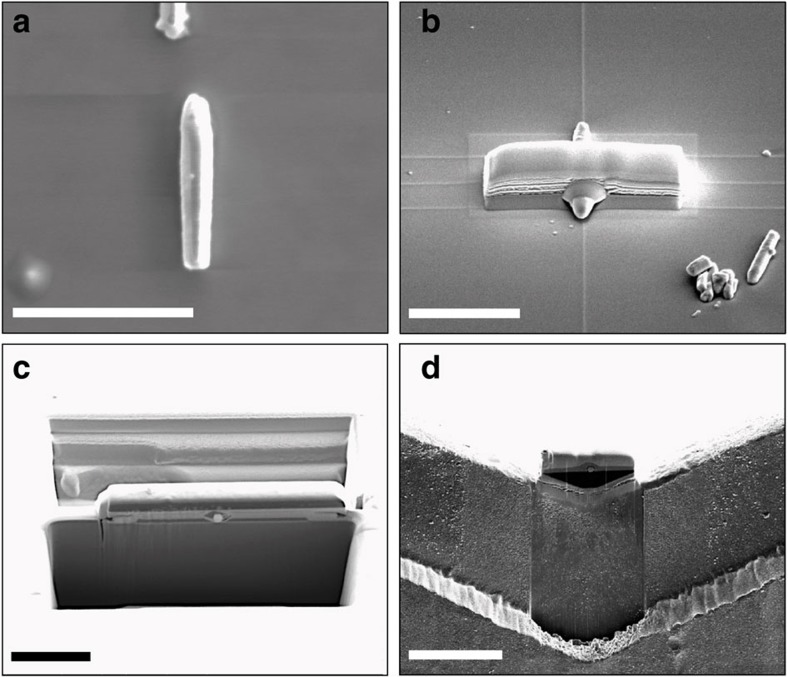
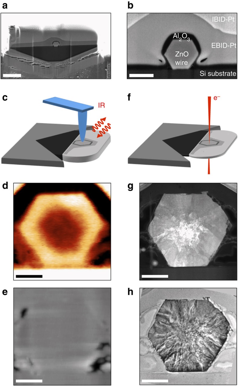
In the next step, we explore the relation between free-carriers density and local crystal structure by correlative IR–electron nanoscopy studies. Because of the strong IR contrast variation between different nanowires in the LED device (Fig. 1), unambiguous conclusions require IR and TEM images of one and the same nanowire cross-section. We show that a suitable sample can be obtained by using focused ion beam (FIB) sample preparation of a nanowire lamella. First, ZnO nanowires are mechanically transferred onto a Si substrate and sputter-coated by a metal oxide (for example, Al2O3 or MgO) layer to protect the nanowires from electron and ion-beam induced crystal damage and possible implantation. Following our particular FIB protocol for TEM sample preparation (see Fig. 2), a thick (~2 μm) lamella containing a cross-section of the ZnO nanowire is prepared. Figure 3a shows a scanning electron microscopy image of the lamella attached to a TEM grid. The hexagonal ZnO nanowire cross-section is clearly visible in between the Si substrate and the Al2O3 coating (Fig. 3b). The lamella is first imaged with IR s-SNOM (Fig. 3c–e) and then thinned from the backside to 20–50 nm to enable high-resolution TEM and scanning TEM (HRTEM and STEM, respectively) imaging (Fig. 3f–h).
Figure 2. Sample preparation for correlative IR–electron nanoscopy.
(a) Two ZnO nanowires on a Si substrate after sputter-coating with a metal oxide (Al2O3) protection layer. (b) Using electron and ion beam-induced deposition (EBID and IBID), respectively, Pt is grown as a second protection layer on top of a selected nanowire. The Pt layer increases the area around the nanowire, which facilitates the s-SNOM imaging of the nanowire cross-section after the final lamella fabrication. (c) FIB milling is used to prepare a lamella containing the nanowire cross-section. (d) Lamella fixed seamlessly to a M-shaped copper grid using IBID-Pt deposition. The seamless attachment of the lamella increases the area for approaching the scanning probe tip to the lamella and thus simplifies s-SNOM imaging. All scale bars denote 5 μm. Note that the images are taken from different nanowires.
Figure 3. Correlative IR–electron nanoscopy of individual ZnO nanowire cross-sections.
(a) Scanning electron microscopy (SEM) image of a FIB prepared lamella that contains a single ZnO nanowire. The scale bar denotes 2 μm. (b) Zoom-in SEM image of the nanowire cross-section. The scale bar denotes 500 nm. (c) Illustration of s-SNOM imaging of the lamella. (d) IR amplitude and (e) topography image of the nanowire cross-section. (f) Illustration of (S)TEM imaging of the lamella. (g) STEM and (h) TEM image of the nanowire cross-section. The scale bars in (d,e,g,h) denote 200 nm.
Figure 3d and e shows the IR near-field amplitude and topography images, respectively, of a representative cross-section of an as-deposited ZnO nanowire. The topography reveals the smooth surface of the lamella with only a few holes (which were formed during the electron beam induced Pt deposition), whereas the IR images exhibit strong materials contrasts between the Al2O3 layer, the Pt coating and the Si substrate. Because of the low near-field signal of Al2O3, we can readily recognize the hexagonal ZnO nanowire. Most importantly, we clearly see that the nanowires exhibit a bright ring surrounding a dark core, resembling the general observations made in Fig. 1a. This finding validates that FIB milling does not alter the free-carrier concentration and distribution significantly. Thus, FIB milling is an appropriate method for the preparation of samples for correlative IR–electron nanoscopy (see Supplementary method section for a detailed discussion of a possible influence of the sample preparation on the IR image contrast). After s-SNOM, we perform ADF STEM (annual dark field STEM, shown in Fig. 3g) and TEM (Fig. 3h; Titan 80-300 G2, FEI, The Netherlands) imaging of the same nanowire cross-section (Fig. 3g,h). Interestingly, the ADF STEM image (Fig. 3g) exhibits a strong contrast between the core and the outer region of the nanowire, although a detailed analysis (see below) shows that the nanowire is mono-crystalline over the whole cross-section. The ADF STEM contrast arises from a high density of nanopores and grain boundaries (see Fig. 4d) in the core of the nanowire. This observation together with previous knowledge50 let us conclude that the fast growth in axial direction is the major cause of defects, whereas the relatively slow shell growth in radial direction allows the formation of an almost defect-free outer shell. More importantly, by comparing both IR s-SNOM and (S)TEM images, we can establish a clear correlation between the local conductivity and local crystal structure: regions of better crystallinity in as-deposited nanowire exhibit a higher conductivity.
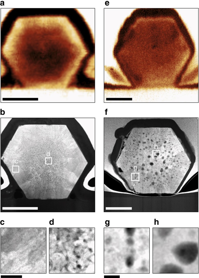
Figure 4. Structure-conductivity relation in ZnO nanowires revealed by IR–electron nanoscopy.
(a) IR near-field amplitude and (b) high-resolution STEM images of an as-deposited ZnO nanowire. (c,d) Enlargements of the regions marked in (b). (e) IR near-field amplitude and (f) STEM images of an annealed ZnO nanowire. (g,h) Enlargements of the regions marked in (f). The nanowire cross-sections were prepared and imaged as described in Fig. 3. The scale bars in (a,b,e,f) denote 250 nm, and in (c,d,g,h) 20 nm.
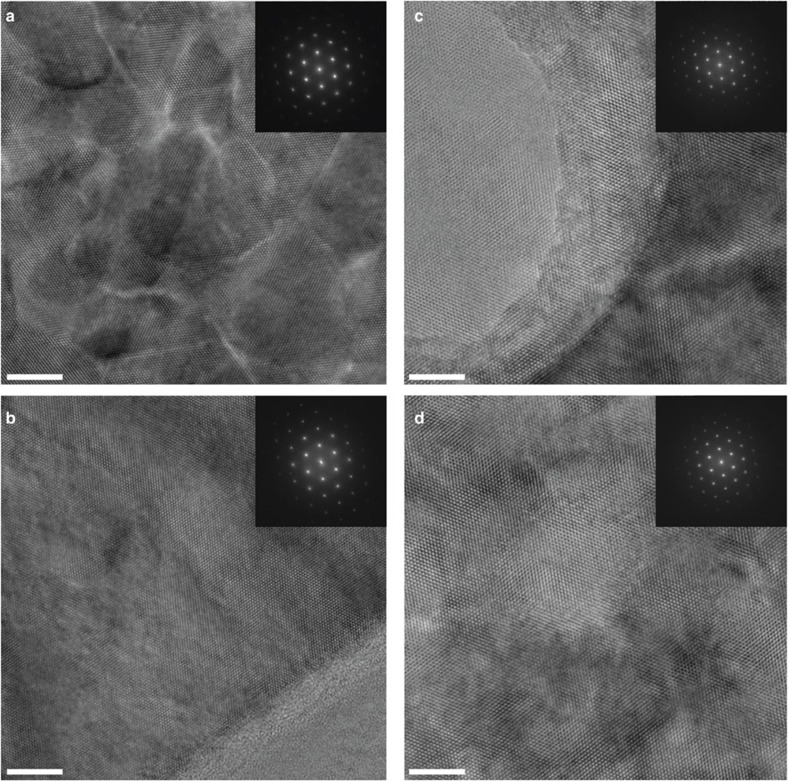
To trace the effect of annealing, we compare cross-sections of as-deposited (Fig. 4a–d) and annealed (Fig. 4e–h) ZnO nanowires. As before in Fig. 1, the radial free-carrier (conductivity) contrast in the s-SNOM images of the as-deposited nanowires (bright ring in Fig. 4a) vanishes after annealing (Fig. 4e), that is, the s-SNOM signal in the nanowire shell decreases. Inside the core, the s-SNOM contrast relative to the Si substrate remains nearly unchanged on annealing. HRTEM images of the same cross-sections (shown in Fig. 5) confirm the mono-crystalline structure of both nanowires. However, the as-deposited nanowire exhibits nanopores and 5–20 nm size grains in its core and a few defects in its shell, as seen in the enlarged high-angular ADF STEM (HAADF STEM) images (Fig. 4c,d). After annealing, we observe large voids in the HAADF STEM images (Fig. 4f–h) with diameters up to 50 nm. The size of the voids decreases in the direction of the nanowire surface. From these HAADF STEM images we conclude that by annealing the large crystal defects (nanopores and grain boundaries) inside the core are transformed into large voids, as seen previously for thin ZnO films55. Within the shell region, the crystal structure remains nearly unchanged on annealing (apart the void formation; see HRTEM images in Fig. 5a and c).
Figure 5. HRTEM images of ZnO nanowire cross-sections.
(a) Image of the core region of the as-deposited ZnO nanowire. Contrast variations over the field of view indicate the presence of a large number of crystal defects, nanopores, probably small angle grain boundaries and threading dislocations. The inset shows a fast Fourier transform (FFT) of the image showing a set of reflections corresponding to [0001] crystallographic zone of ZnO. The slight azimuthal elongation of reflections in FFT reveals a mutual rotation of parts of the crystal lattice in the core, amounting to a few degrees. (b) Image of the shell region of the as-deposited ZnO nanowire, showing an almost defect-free crystal structure. (c) Image of the core region of the annealed ZnO nanowire, showing that large voids (bright region at the left part of the image) have been formed. The FFT analysis displays a good crystallinity. The absence of a crystal rotation substantiates that grain boundaries vanish after annealing. (d) Image of the shell region of the annealed ZnO nanowire, showing a small number of voids (bright region in the centre of view), however, much smaller in size than the voids in the core (Fig. 5c). The FFT analysis confirms the good crystallinity, and shows that annealing did not change the crystal structure. All scale bars denote 5 nm.
Discussion
The correlation of both IR and (S)TEM images yields interesting insights into the local structure–conductivity relationship of the nanowires. The bright ring in the s-SNOM images of the as-deposited nanowire (Figs 1a–c and 4a) reveals a large amount of free-carriers (high conductivity) in the shell region, which due to the nearly perfect crystal structure we can assign to point defects (vacancies, interstitials and extrinsic dopants, such as hydrogen, not seen in (S)TEM) acting as free-carrier donors. The low conductivity (low IR signal) in the core of the as-deposited nanowire, (Figs 1a–c and 4a) we can explain either by a lower free-carrier concentration due to trapping of free carriers at the grain boundaries, or by a reduced free-carrier mobility due to scattering at grain boundaries. On annealing, the vanishing bright ring in the s-SNOM images (Figs 1d–f and 4e) reveals that the free-carrier concentration in the shell region is reduced (as discussed before with the help of Fig. 1h). Because of the unchanged crystal structure in the shell, we can thus conclude that annealing reduces the point defects (free-carrier donors) in the shell. In the core of the annealed nanowire we find a clearly improved crystallinity (see Fig. 5c). The carrier mobility is thus expected to increase, which would come along with an increase of the near-field amplitude and phase (see Fig. 1g). However, the near-field amplitude and phase in the core do not change on annealing, which lets us conclude that the free-carrier concentration is below 1018 carriers cm−3, where any change of the mobility is not detectable.
Our observations provide detailed and spatially resolved insights into the nanowire growth and how annealing affects the free-carrier distribution in unintentionally doped ZnO nanowires. This knowledge will be essential for optimizing ZnO nanowires for applications in (opto-)electronic devices. On the other hand, our studies reveal that a large local free-carrier concentration within a nearly perfect crystalline structure can be achieved by lateral nanowire growth. Such nanowires are highly interesting for applications where a high conductivity simultaneously to optical transparency is required (for example, transparent electrodes). Furthermore, our findings explain why etching of as-deposited ZnO nanowires yields tailored ZnO nanotubes56,57,58: because of its high defect density, the core is strongly and selectively etched, leaving an almost defect-free outer shell.
In conclusion, we have demonstrated correlative IR–electron nanoscopy, a novel analytical imaging tool providing nanoscale-resolved IR images and atomically resolved TEM images of one and the same nanostructures. Applying it to ZnO nanowires, we obtained nanoscale-resolved real-space maps of radial free-carrier distributions, exhibiting a clear correlation to structural defects seen by TEM. We point out that correlative IR–electron nanoscopy has a wide application potential far beyond nanowire research. We envision highly interesting and novel insights into exotic conductors, such as graphene or topological insulators, where the interplay between local conductivity and local crystal structure is a widely unexplored terrain. Because of the high chemical sensitivity of IR light, correlative IR–electron nanoscopy could be also applied for combined nanoscale chemical and structural mapping of organic and biological matter.
Methods
IR s-SNOM
The setup comprises a s-SNOM (from Neaspec GmbH), which is based on an AFM. The AFM tip is illuminated with the focused beam of a CO2 laser operating at 10.74 μm. Operating the AFM in tapping mode, the tip is vertically vibrating with an amplitude of about 60 nm at a frequency of Ω≈300 kHz. Background-free near-field IR imaging is achieved by pseudo-heterodyne interferometric detection of the backscattered light and subsequent demodulation of the detector signal at the n-th harmonic of the tapping frequency, n·Ω. In the present experiments, the signal amplitude s3 and phase Φ3 images (n=3) were recorded simultaneously with the AFM topography.
Electrodeposition of ZnO nanowire arrays
ZnO nanowire arrays were electrodeposited from the reduction of dissolved molecular oxygen in zinc chloride aqueous solutions59,60.The electrodeposition experiment was performed in a three-electrode electrochemical setup using a VMP3 BioLogic-Science Multichannel Workstation. The cathode was a commercial conducting glass/SnO2:F (TEC15, Hartford Glass Co) substrate. A Pt spiral wire was used as the anode and a saturated calomel electrode as the reference electrode. The electrolyte was a 5×10⁻⁴ M ZnCl2 (>98.0 %), 3.4 M KCl (>99.5 %) ultrapure aqueous solution, saturated with bubbling oxygen. The electrodeposition was performed at 80 °C under constant potential (V~−1.0 V versus saturated calomel electrode).
Annealing of ZnO nanowire arrays
The post-deposition thermal annealing was performed in an open horizontal tubular furnace. The ZnO nanowire arrays were air annealed at 450 °C during 1 h.
Deposition of metal oxide protection layer
The metal oxide (Al2O3 or MgO) protection layer was deposited by radio frequency magnetron sputtering at room temperature and at a pressure of 3 mTorr. We emphasize that in case of the annealed nanowires, the coating of the nanowires was performed after annealing to avoid diffusion between ZnO and the coating.
Author contributions
R.H. developed the concept of correlative IR–electron nanoscopy and together with J.M.S., R.T.-Z. and A.C. conceived and designed the experiments. R.T.-Z. grew the ZnO nanowire arrays and ZnO/CuSCN heterostructures. J.M.S. performed the s-SNOM experiments and calculations. A.C. prepared the FIB lamellas and performed the TEM studies. J.M.S. and O.I. contributed to sample preparation. All authors analysed and discussed the data. R.H. wrote the manuscript together with J.M.S., supported by R.T.-Z. and A.C.
Additional information
How to cite this article: Stiegler J. M. et al. Correlative infrared–electron nanoscopy reveals the local structure–conductivity relationship in zinc oxide nanowires. Nat. Commun. 3:1131 doi: 10.1038/ncomms2118 (2012).
Supplementary Material
Supplementary Figure S1, Supplementary Methods and Supplementary References
Acknowledgments
We thank Christopher Tollan for help with the fabrication of mechanically polished samples. This study was financially supported by the Spanish Ministerio de Ciencia e Innovacion (Projects MAT2009-08398 and HOPE CSD2007-0007 (Consolider-Ingenio 2010)) and the Basque Government (nanoIKER Etortek). R.T-Z. acknowledges the support of the Programme Ramón y Cajal. O.I. acknowledges the Basque Government for fellowship no. BFI09.284. We also acknowledge financial support from FEI Company (The Netherlands) within the framework of a collaborative project.
Footnotes
R.H. is co-founder of Neaspec GmbH, a company producing s-SNOM systems, such as the one used in this study. The remaining authors declare no competing financial interests.
References
- Williams D. B. & Carter C. B. Transmission Electron Microscopy 2 edn, (Springer, 2009). [Google Scholar]
- Meyer E., Hug H. J. & Bennewitz R. Scanning Probe Microscopy 1 edn. (Springer, 2004). [Google Scholar]
- Mikkelsen A. et al. Direct imaging of the atomic structure inside a nanowire by scanning tunnelling microscopy. Nat. Mater. 3, 519–523 (2004). [DOI] [PubMed] [Google Scholar]
- Mikkelsen A., Skold N., Ouattara L. & Lundgren E. Nanowire growth and dopants studied by cross-sectional scanning tunnelling microscopy. Nanotechnology 17, S362–S368 (2006). [Google Scholar]
- Hansma P. K., Elings V. B., Marti O. & Bracker C. E. Scanning tunneling microscopy and atomic force micrsocopy—application to biology and technology. Science 242, 209–216 (1988). [DOI] [PubMed] [Google Scholar]
- Widrig C. A., Alves C. A. & Porter M. D. Scanning tunneling microscopy of ethanethiolate and normal-octadecanethiolate monolayers spontaneously adsorbed at gold surfaces. J. Am. Chem. Soc. 113, 2805–2810 (1991). [Google Scholar]
- Stipe B. C., Rezaei M. A. & Ho W. Single-molecule vibrational spectroscopy and microscopy. Science 280, 1732–1735 (1998). [DOI] [PubMed] [Google Scholar]
- Kawata S. & Inouye Y. Scanning probe optical microscopy using a metallic probe tip. Ultramicroscopy 57, 313–317 (1995). [Google Scholar]
- Bachelot R., Gleyzes P. & Boccara A. C. Near-field optical microscope based on local perturbation of a diffraction spot. Opt. Lett. 20, 1924–1926 (1995). [DOI] [PubMed] [Google Scholar]
- Zenhausern M., Martin Y. & Wickramasinghe H. K. Scanning interferometric apertureless microscopy: optical imaging at 10 angstrom resolution. Science 269, 1083–1085 (1995). [DOI] [PubMed] [Google Scholar]
- Knoll B. & Keilmann F. Near-field probing of vibrational absorption for chemical microscopy. Nature 399, 134–137 (1999). [Google Scholar]
- Hillenbrand R., Taubner T. & Keilmann F. Phonon-enhanced light-matter interaction at the nanometre scale. Nature 418, 159–162 (2002). [DOI] [PubMed] [Google Scholar]
- Huber A. J., Keilmann F., Wittborn J., Aizpurua J. & Hillenbrand R. Terahertz near-field nanoscopy of mobile carriers in single semiconductor nanodevices. Nano Lett. 8, 3766–3770 (2008). [DOI] [PubMed] [Google Scholar]
- Taubner T., Hillenbrand R. & Keilmann F. Nanoscale polymer recognition by spectral signature in scattering infrared near-field microscopy. Appl. Phys. Lett. 85, 5064–5066 (2004). [Google Scholar]
- Raschke M. B. et al. Apertureless near-field vibrational imaging of block-copolymer nanostructures with ultrahigh spatial resolution. ChemPhysChem 6, 2197–2203 (2005). [DOI] [PubMed] [Google Scholar]
- Huth F. et al. Nano-FTIR absorption spectroscopy of molecular fingerprints at 20 nm spatial resolution. Nano Lett. 12, 3973–3978 (2012). [DOI] [PubMed] [Google Scholar]
- Huber A. J., Kazantsev D., Keilmann F., Wittborn J. & Hillenbrand R. Simultaneous IR material recognition and conductivity mapping by nanoscale near-field microscopy. Adv. Mater. 19, 2209–2212 (2007). [Google Scholar]
- Samson J.- S. et al. Setup of a scanning near field infrared microscope (SNIM): imaging of sub-surface nano-structures in gallium-doped silicon. Phys. Chem. Chem. Phys. 8, 753–758 (2006). [DOI] [PubMed] [Google Scholar]
- Qazilbash M. M. et al. Mott transition in VO2 revealed by infrared spectroscopy and nano-imaging. Science 318, 1750–1753 (2007). [DOI] [PubMed] [Google Scholar]
- Stiegler J. M. et al. Nanoscale free-carrier profiling of individual semiconductor nanowires by infrared near-field nanoscopy. Nano Lett. 10, 1387–1392 (2010). [DOI] [PubMed] [Google Scholar]
- Sanchez E. J., Novotny L. & Xie X. S. Near-field fluorescence microscopy based on two-photon excitation with metal tips. Phys. Rev. Lett. 82, 4014–4017 (1999). [Google Scholar]
- Cvitkovic A., Ocelic N., Aizpurua J., Guckenberger R. & Hillenbrand R. Infrared imaging of single nanoparticles via strong field enhancement in a scanning nanogap. Phys. Rev. Lett. 97, 060801 (2006). [DOI] [PubMed] [Google Scholar]
- Brehm M., Schliesser A., Cajko F., Tsukerman I. & Keilmann F. Antenna-mediated back-scattering efficiency in infrared near-field microscopy. Opt. Express 16, 11203–11215 (2008). [DOI] [PubMed] [Google Scholar]
- Stockle R. M., Suh Y. D., Deckert V. & Zenobi R. Nanoscale chemical analysis by tip-enhanced Raman spectroscopy. Chem. Phys. Lett. 318, 131–136 (2000). [Google Scholar]
- Hartschuh A., Sanchez E. J., Xie X. S. & Novotny L. High-resolution near-field Raman microscopy of single-walled carbon nanotubes. Phys. Rev. Lett. 90, 095503 (2003). [DOI] [PubMed] [Google Scholar]
- Anderson M. S. Locally enhanced Raman spectroscopy with an atomic force microscope. Appl. Phys. Lett. 76, 3130–3132 (2000). [Google Scholar]
- Hayazawa N., Inouye Y., Sekkat Z. & Kawata S. Near-field Raman scattering enhanced by a metallized tip. Chem. Phys. Lett. 335, 369–374 (2001). [Google Scholar]
- Keilmann F. & Hillenbrand R. Near-field microscopy by elastic light scattering from a tip. Philos. T. Roy. Soc. A 362, 787–805 (2004). [DOI] [PubMed] [Google Scholar]
- Huber A. J., Ziegler A., Kock T. & Hillenbrand R. Infrared nanoscopy of strained semiconductors. Nat. Nanotech. 4, 153–157 (2009). [DOI] [PubMed] [Google Scholar]
- Kehr S. C. et al. Anisotropy contrast in phonon-enhanced apertureless near-field microscopy using a free-electron laser. Phys. Rev. Lett. 100, 256403 (2008). [DOI] [PubMed] [Google Scholar]
- Cvitkovic A., Ocelic N. & Hillenbrand R. Material-specific infrared recognition of single sub-10 nm particles by substrate-enhanced scattering-type near-field microscopy. Nano Lett. 7, 3177–3181 (2007). [DOI] [PubMed] [Google Scholar]
- Akhremitchev B. B., Sun Y., Stebounova L. & Walker G. C. Monolayer-sensitive infrared imaging of DNA stripes using apertureless near-field microscopy. Langmuir 18, 5325–5328 (2002). [Google Scholar]
- Arsov Z., Quaroni L. & Havenith M. Nanoscale depth resolution in scanning near-field infrared microscopy. Opt. Express 16, 7453–7459 (2008). [DOI] [PubMed] [Google Scholar]
- Ogawa Y., Minami F., Abate Y. & Leone S. R. Nanometer-scale dielectric constant of Ge quantum dots using apertureless near-field scanning optical microscopy. Appl. Phys. Lett. 96, 063107 (2010). [Google Scholar]
- Knoll B. & Keilmann F. Infrared conductivity mapping for nanoelectronics. Appl. Phys. Lett. 77, 3980–3982 (2000). [Google Scholar]
- Spirkoska D. et al. Structural and optical properties of high quality zinc-blende/wurtzite GaAs nanowire heterostructures. Phys. Rev. B 80, 245325 (2009). [Google Scholar]
- Lopez F. J., Hemesath E. R. & Lauhon L. J. Ordered stacking fault arrays in silicon nanowires. Nano Lett. 9, 2774–2779 (2009). [DOI] [PubMed] [Google Scholar]
- Lim S. K. et al. Direct correlation between structural and optical properties of III-V nitride nanowire heterostructures with nanoscale resolution. Nano Lett. 9, 3940–3944 (2009). [DOI] [PubMed] [Google Scholar]
- Heiss M. et al. Direct correlation of crystal structure and optical properties in wurtzite/zinc-blende GaAs nanowire heterostructures. Phys. Rev. B 83, 045303 (2011). [Google Scholar]
- Schroer M. D. & Petta J. R. Correlating the nanostructure and electronic properties of InAs nanowires. Nano Lett. 10, 1618–1622 (2010). [DOI] [PubMed] [Google Scholar]
- Thelander C., Caroff P., Plissard S., Dey A. W. & Dick K. A. Effects of crystal phase mixing on the electrical properties of InAs nanowires. Nano Lett. 11, 2424–2429 (2011). [DOI] [PubMed] [Google Scholar]
- Sartori A. et al. Correlative microscopy: bridging the gap between fluorescence light microscopy and cryo-electron tomography. J. Struct. Biol. 160, 135–145 (2007). [DOI] [PubMed] [Google Scholar]
- Polishchuk R. S. et al. Correlative light-electron microscopy reveals the tubular-saccular ultrastructure of carriers operating between Golgi apparatus and plasma membrane. J. Cell Biol. 148, 45–58 (2000). [DOI] [PMC free article] [PubMed] [Google Scholar]
- Könenkamp R., Word R. C. & Godinez M. Ultraviolet electroluminescence from ZnO/polymer heterojunction light-emitting diodes. Nano Lett. 5, 2005–2008 (2005). [DOI] [PubMed] [Google Scholar]
- Xu S. et al. Self-powered nanowire devices. Nat. Nanotechnol. 5, 366–373 (2010). [DOI] [PubMed] [Google Scholar]
- Xu J. et al. Arrays of ZnO/ZnxCd1−xSe nanocables: band gap engineering and photovoltaic applications. Nano Lett. 11, 4138–4143 (2011). [DOI] [PubMed] [Google Scholar]
- Vayssieres L. Growth of arrayed nanorods and nanowires of ZnO from aqueous solutions. Adv. Mater. 15, 464–466 (2003). [Google Scholar]
- Joo J., Chow B. Y., Prakash M., Boyden E. S. & Jacobson J. M. Face-selective electrostatic control of hydrothermal zinc oxide nanowire synthesis. Nat. Mater. 10, 596–601 (2011). [DOI] [PMC free article] [PubMed] [Google Scholar]
- Peulon S. & Lincot D. Cathodic electrodeposition from aqueous solution of dense or open-structured zinc oxide films. Adv. Mater. 8, 166–170 (1996). [Google Scholar]
- Tena-Zaera R., Elias J., Wang G. & Levy-Clement C. Role of chloride ions on electrochemical deposition of ZnO nanowire arrays from O2 reduction. J. Phys. Chem. C 111, 16706–16711 (2007). [Google Scholar]
- Zhang Q. et al. n-ZnO nanorods/p-CuSCN heterojunction light-emitting diodes fabricated by electrochemical method. Electrochim. Acta 55, 4889–4894 (2010). [Google Scholar]
- Cvitkovic A., Ocelic N. & Hillenbrand R. Analytical model for quantitative prediction of material contrasts in scattering-type near-field optical microscopy. Opt. Express 15, 8550–8565 (2007). [DOI] [PubMed] [Google Scholar]
- Itoh T. et al. Optical properties of conductive ZnO films near infrared frequency. Phys. Status Solidi C 6, S110–S113 (2009). [Google Scholar]
- Tena-Zaera R. et al. Influence of the potassium chloride concentration on the physical properties of electrodeposited ZnO nanowire arrays. J. Phys. Chem. C 112, 16318–16323 (2008). [Google Scholar]
- Richardson J. J. et al. Thermally induced pore formation in epitaxial ZnO films grown from low temperature aqueous solution. Cryst. Growth Des. 11, 3558–3563 (2011). [Google Scholar]
- Vayssieres L., Keis K., Hagfeldt A. & Lindquist S.- E. Three-dimensional array of highly oriented crystalline ZnO microtubes. Chem. Mater. 13, 4395–4398 (2001). [Google Scholar]
- Elias J., Tena-Zaera R., Wang G.- Y. & Lévy-Clément C. Conversion of ZnO nanowires into nanotubes with tailored dimensions. Chem. Mater. 20, 6633–6637 (2008). [Google Scholar]
- She G.- W. et al. Controlled synthesis of oriented single-crystal ZnO nanotube arrays on transparent conductive substrates. Appl. Phys. Lett. 92, 053111–053113 (2008). [Google Scholar]
- Peulon S. & Lincot D. Mechanistic study of cathodic electrodeposition of zinc oxide and zinc hydroxychloride films from oxygenated aqueous zinc chloride solutions. J. Electrochem. Soc. 145, 864–874 (1998). [Google Scholar]
- Tena-Zaera R. et al. Electrodeposition and impedance spectroscopy characterization of ZnO nanowire arrays. Phys. Status Solidi A 205, 2345–2350 (2008). [Google Scholar]
Associated Data
This section collects any data citations, data availability statements, or supplementary materials included in this article.
Supplementary Materials
Supplementary Figure S1, Supplementary Methods and Supplementary References


