Abstract
Asymmetric light propagation is crucial to the development of optical-based functional components in nanophotonics. Diverse configurations and structures have been proposed to allow asymmetrical propagation of photonic signal, but on-chip integration is difficult to achieve due to their complex structure and/or relatively large footprint. Here we report the first design and realization of asymmetric light propagation in single semiconductor nanowires with a composition gradient along the length. We show the asymmetric nanowire waveguides can be synthesized using a simple thermal evaporation and vapor transport approach without involving complicated and costly fabrication processes. Our studies demonstrate the asymmetric nanowire waveguides offer some significant advantages over previous designs, including ultra-low operation power, tunable working wavelength and nanoscale footprint, making them attractive building blocks for integrated photonic circuits.
Structures that allow unidirectional propagation of electrical current represent the most fundamental building blocks for all-semiconductor electronic devices and circuits, including transistors and logic gates that are responsible for the revolution of electrical computing and information technology in the past half century. Stimulated by the widespread applications of this one-way propagation of electrical current, several other counterpart devices with unidirectional transport of heat flow1,2 and acoustic energy flux3,4 have been recently demonstrated. Similarly, considerable effort has been dedicated to the study of asymmetric (unidirectional) light propagation or photonic rectification5,6,7,8,9,10,11,12, which may find potential applications in developing next generation of all-optical computing and processing devices and system. A number of asymmetric configurations and/or nonlinear structures have been proposed for unidirectional optical action, including planar chiral structure5,6, liquid crystal heterojunctions7, photonic crystals13,14,15, absorbing multilayer structures16, concentration-gradient fluorescent dyes17, asymmetric optical resonators18 and so on8,10,19,20. However, these reported schemes to date often suffer from the requirement of complex structures, costly fabrication processes, high operation threshold intensity and poor non-reciprocities, which have seriously limited their potential applications. Additionally, most of these structures take too large a footprint to be suitable for applications in on-chip photonic circuits.
With the unique one-dimensional (1D) structural characteristics and versatile physical/chemical properties, semiconductor nanowires have emerged as the building blocks for a variety of fundamental optical components, including nanoscale lasers21,22,23,24, photodetectors25 and optical waveguides26,27. However, asymmetric light propagation has not yet been realized in common composition-homogeneous nanowires owing to the difficulty in breaking time reversal symmetry of light-matter interaction9,10,13,15.
Here we report for the first time the design and realization of asymmetric light propagation in single composition-graded semiconductor nanowires. The absorption or loss of the guided light within the wires is highly dependent on the propagation direction as a result of the existence of the intrinsic spatially-graded composition and bandgap along their length, which provides the physical base of the asymmetric light propagation. These graded nanowire-based asymmetric waveguides feature simple fabrication process, ultra-low operating power, readily tunable working wavelength and nanoscale footprint, making them attractive candidates for straightforward nanophotonic applications.
Results
Theoretical design of asymmetric light propagation
In composition-homogeneous nanostructures, asymmetric light propagation is hardly achievable as a result of the time reversal symmetry of light-matter interaction. Here we consider semiconductor alloy nanowires with a spatial composition/bandgap gradient along their length direction. As schematically shown in Fig. 1a, the energy gap at a local position l of a composition-graded nanowire with a length of L, Eg(l), gradually increases from left (Eg(0)) to right (Eg(L)) along its length. According to the fundamental theory of 1D semiconductor waveguides27,28,29, the spectrum at the position l (propagation length) of the nanowire can be written as
where S0 is the input spectrum at the initial position l = 0, α(hv) is the optical absorption coefficient, which can be given with different expressions at different energy scale27,28,29
where A0 is a structure-related constant, kT is the thermal energy at room temperature, h is Planck's constant, v is the photon frequency and σ is a composition-dependent dimensionless phenomenological fitting parameter.
Figure 1. Theoretical design of asymmetric light propagation.
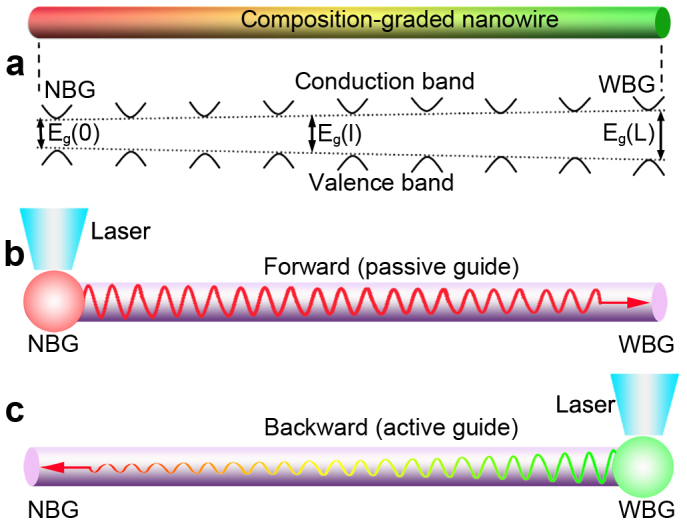
(a) Schematic diagrams of a composition-graded nanowire and its corresponding bandgap structure. (b, c) Schematic illustration of asymmetric light propagation mechanism.
When the narrow bandgap (NBG) end of the nanowire is locally excited by a focused laser (Fig. 1b), the photon energy (E) of the emitted light from near-bandedge states is smaller than the bandgap energy of any other positions along the nanowire, and the absorption equation (2) dominates the light-matter interaction process while the light is propagating along the bandgap-increasing direction (forward). In this case, interband optical absorption cannot take place and the nanowire acts as a passive optical cavity. The guided light will transmit mainly through total internal reflections, just like light transmits in a transparent optical fiber. The propagation loss (both the optical intensity and the photon energy) is dominated by the disorder-induced band-tail absorption and non-perfect geometry-caused leakage, which should be relatively small for high-quality nanowire waveguides (smooth surface, uniform diameter and high crystallinity). In comparison, when the wide bandgap (WBG) end of the nanowire is excited with the same power (Fig. 1c), the situation, however, is entirely different. The emitted light would be guided toward the NBG end mainly obeying the absorption equation (3) since the photon energy (E) of the guided light is larger than the bandgap energy of any positions along the guiding media. Here the nanowire acts as an active optical cavity and the excited light will travel along the bandgap-decreasing direction (backward) through incessantly repeated band-to-band re-absorption and re-emitting processes27. During this active propagation, the wavelength of the guided light will change and redshift continuously. Despite the same propagation loss from structural disorder or surface scattering as the passive waveguiding along the opposite direction, the total loss in this case would be significantly increased, coming from the nonradiative loss involved in each band-to-band re-absorption and re-emitting process.
On the basis of the above discussion, the light propagation mechanisms along the two opposite directions of the same nanowire are totally different, with much lower optical loss along the forward direction than that of backward direction. Therefore, the intensity of the optical signal after the forward propagation is expected to be much higher than that of the backward propagation, resulting in a strong intensity contrast, which provides a new working principle for realizing asymmetric light propagation and maybe hold significant potential for future integrated photonic circuits.
Experimental realization of asymmetric light propagation
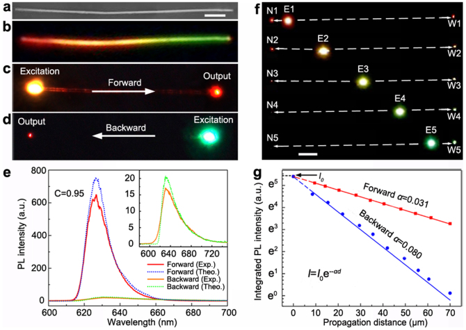
To realize the asymmetric light propagation in semiconductor nanowires, composition-graded CdSxSe1-x alloy nanowires were grown via an evaporation source controlled (with a moving source) CVD route30,31. The bandgap of these nanowires can be maximally tuned from ~2.42 eV (x = 1, WBG end) to ~1.74 eV (x = 0, NBG end) along their axial directions. Moreover, the specific bandgap variation (both tunable range and gradient) of the grown nanowires can be well controlled by precisely adjusting the growth parameters (pressure, growth time and the moving speed of source boats). Fig. 2a shows the SEM observation of a representative composition-graded CdSSe nanowire (70 μm long and 400 nm in width with uniform diameter). The position dependent micro-EDS information confirms that the contents of S and Se elements are gradually changed along the length of the nanowire (see Supplementary Fig. S1). Under the illumination of a diffused laser (405 nm), the exhibited photoluminescence (PL) color of the wire is continuously varied from green to red along its entire length (Fig. 2b), with the PL peak wavelength spanning from ~520 nm to ~625 nm along its entire length (see Supplementary Fig. S2). Fig. 2c and 2d give the real-color PL photographs of the nanowire excited with a focused laser (488 nm, photon energy above the WBG) at one of its ends, respectively. The excitation power densities were kept the same for effectively contrasting the detected signals at the two opposite output ends. As shown in the photographs, the forward output end has a large and bright light spot, which shows significant contrast with the small and obscure one at the backward output end. This observation clearly indicates that the propagation efficiencies along the two opposite directions are entirely different. The corresponding PL spectra further quantitatively demonstrate that the total integrated intensity of the forward output light is forty times stronger than that of the backward one (Fig. 2e), demonstrating the propagation efficiency of these nanowires is highly sensitive to the propagation direction. To quantitatively estimate the asymmetry of the light propagation, we defined the intensity contrast (C) between the two output end as, C = (I+−I−)/(I++I−), where I+ and I− are the forward and backward output intensity, respectively20. According to this definition, the calculated C value of the examined nanowire reaches 0.95. After examining dozens of such composition-graded nanowires, the obtained intensity contrasts usually varied from 0.8 to 0.97, which further confirms that these nanowires possess excellent asymmetric light propagation ability.
Figure 2. Experimental and theoretically simulated performance of asymmetric light propagation.
(a) SEM image of an examined composition-graded nanowire. Scale bar, 7 μm. (b) Real-color PL photograph of the nanowire under the illumination of a diffused 405-nm semiconductor laser, taken with a 405-nm notch filter. (c, d) Real-color PL photographs with local excitation at one of its ends. (e) Corresponding PL spectra at the output ends. The solid lines (red and orange) represent the experimental results and dashed lines (blue and green) representing the theoretical results, respectively. Inset is the enlarged backward output PL spectra. See Supplementary Fig. S4 for more simulation details. (f) Real-color PL photographs of the nanowire, with local excitation at different spots (E1–E5) along its length. W1–W5 and N1–N5 showing the emission of the guided light at the WBG and NBG ends, respectively. Scale bar, 7 μm. (g) Propagation distance-dependent PL integrated intensity (integral area) at the WBG end (forward) and the NBG end (backward), respectively.
To study the propagation efficiency along the two opposite directions, the nanowire was locally excited in turn at various positions (E1–E5 in Fig. 2f) along its length by the same focused laser (488 nm) and the output optical signals from its both ends (W1–W5 and N1–N5 in Fig. 2f) were detected simultaneously (see Supplementary Fig. S3 for the corresponding PL spectra). Fig. 2g gives the propagation distance-dependent PL integrated intensity (integral area of each detected PL spectra) for the both propagation directions. Each of them can be well fitted into an exponential decay function, I = I0e−αd, where I0 is the initial intensity, d is the propagation distance, α is the decay coefficient. The results show that the decay coefficient of the backward propagation (0.080) is much larger than that of the forward propagation (0.031). It is this large difference of the intensity decay that results in the large intensity contrast in the output signals, and provides the working principle for the nanowire-based asymmetric waveguides.
Theoretical simulation of asymmetric light propagation
The asymmetric light propagation in these composition-graded nanowires can be further quantitatively confirmed using the finite element simulation on the basis of the fundamental optical absorption theory of semiconductors27,28,29. Supposing the graded nanowire with length L is divided into n sections, each section can be considered as a composition-homogenous medium as long as L/n is small enough. Therefore, the bandgap within i section, Eg(i), is a constant value, which can be given as
The spectrum Si after transmit i sections will be given by
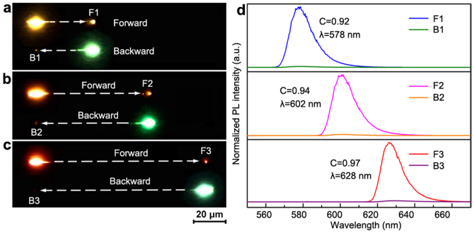
where αi(hv) is the absorption coefficient within the i section, which can be calculated according to equation (2) and (3) for different energy scale. For the examined nanowire in Fig. 2, L = 70 μm, Eg(0) = 2.05 eV, Eg(L) = 2.39 eV, A0 = 3×104 cm−1·eV−1/2, kT = 25 meV, and n = 70. S0 for equation (4) is the intensity-normalized near-bandedge emission at the two ends and σ is composition-dependent (see Supplementary Fig. S4). The output spectra after the two opposite propagations along the nanowire were individually simulated and shown in Fig. 2e. The lineshape and the spectrum position of the simulated results (dash lines) are in good agreement with the experiments (solid lines) for both the forward and the backward output signals. The slightly larger decrease of the optical intensity observed in experiment than that in simulation can be attributed to the imperfection or geometry structure induced energy loss at the surfaces. These analyses confirm definitely that the graded bandgap structure provides the physical basis for the asymmetric light propagation. In addition, both the experiments and the simulations further show that the detected signals from the two output ends of the examined wire have the same peak wavelength (~625 nm), which is determined by the bandgap of its NBG end. On the basis of this principle, the working wavelength of this asymmetric light propagation can be tuned by using nanowires with different compositions (bandgaps) at the NBG end. Fig. 3a–c show the real-color images of three representative results, with their working wavelength at 578, 602 and 628 nm, respectively (Fig. 3d).
Figure 3. Asymmetric waveguides with variable working wavelengths.
(a–c) Real-color PL photographs. The outlines of the nanowires are tracked with dashed arrows. (d) Corresponding output spectra for both forward and backward propagations. The spectra were normalized in intensity, and vertically shifted for clarity.
Excitation wavelength and power dependent performance of asymmetric light propagation
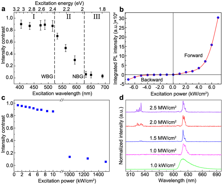
It is worth noting that all the above discussion and results are based on the excitation energies above the WBG of the wire. What would be happen if the excitation energies below the WBG? Fig. 4a shows the excitation wavelength dependent intensity contrast of the nanowire waveguide, which indicates that the asymmetric performance is highly sensitive to the excitation wavelength (energy). For excitation energies above the WBG (Zone I in Fig. 4a), the nanowire waveguides exhibit excellent asymmetric effect, with the obtained C values typically larger than 0.80. When the excitation energy is located between the WBG and the NBG (Zone II in Fig. 4a), the intensity contrast gradually decreases with lowering the excitation energy, denotes the asymmetric effect is gradually “turn off”. When the excitation energies is bellow the NBG (Zone III in Fig. 4a), the intensity contrast turns to be very small, which means the asymmetric effect almost completely disappeared. As discussed previously in this paper, the asymmetric propagation effect of these composition graded wires is related to the active propagation at the backward direction. When the excitation energy is below the WBG, the active propagation distance decreases with reducing the excitation energy, leading to the weakening of the asymmetric effect (Fig. 4a). For more details about the interpretation of this excitation energy dependent intensity contrast, see Supplementary Fig. S5 and its corresponding discussion.
Figure 4. Excitation wavelength and power dependent performance of asymmetric waveguide.
(a) Excitation wavelength dependent intensity contrast. The error bar for each excitation wavelength is obtained from the statistical results of 10 nanowires. (b) Excitation power dependent output intensity. The positive and negative excitation power denote the excitation at the NBG end and WBG end, respectively, and the positive and negative PL intensities denote the output intensities at the WBG end and the NBG end, respectively. The dots are experimental results and the lines are exponential fitting results. (c) Excitation power dependent intensity contrast at the two ends. (d) Backward output spectra (at the NBG end) of the asymmetric waveguide with different pumping power density at the WBG end. The spectra were normalized in intensity and vertically shifted for clarity.
We have also investigated the excitation power dependent light propagation characteristics along these composition graded wires. Here we define the excitation at the NBG end and WBG end as the positive and negative excitation, respectively, and the output intensities at the WBG end and the NBG end as positive and negative PL intensities, respectively. According to this definition, the plot of the power-dependent output intensity for both the forward and the backward propagation is very similar to the characteristic curve of a rectifier (Fig. 4b), which further confirms the excellent asymmetric effect of these wires. The power-dependent intensity contrast (Fig. 4c) reveals that the asymmetric propagation ability is well preserved at low excitation power (<10 kW/cm2) but decreases at high power (>1 MW/cm2). The low operating power is important for applications in nanophotonics12,14,20,24. The decreasing intensity contrast with the increasing excitation power is attributed to the absorption saturation effect32 of the backward active propagation at high excitation power, which can be further demonstrated by exciting the WBG end of the wire under very high powers. As shown in Fig. 4d, when the excitation was increased to 1 MW/cm2, the linewidth of the backward output signal narrowed significantly, indicating the output signal has undergone the transition from spontaneous emission to stimulated emission21,22,23,24. More interestingly, further elevating the pumping power to an extremely high level (~1.5 MW/cm2), some new emission lines from the in situ excited PL (centered at ~520 nm) at the WBG end were simultaneously detected from the backward output signal at the NBG end, indicating that the absorption at the backward active process was completely saturated. In this case, the guided light can no longer hold the unidirectional propagation ability, in analogy to the electrical breakdown of an electronic diode at high reverse electric bias voltage.
Asymmetric light propagation in branched nanowire structure
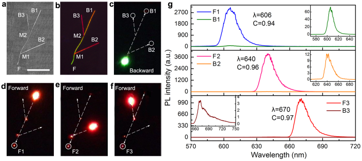
As described in the previous section (Fig. 2e and Fig. 3), the output wavelength of the asymmetric guiding is determined by the bandgap energy at the NBG end of the nanowires, independent from the bandgap value at the WBG end. At the same time, the wavelength of the guided light continuously change (redshift) during the active propagation along the bandgap-decreased direction of the wire, which was well demonstrated by the simulated results27 (see Supplementary Fig. S6). On the basis of these principles, asymmetric waveguides with different working wavelengths is expected to be simultaneously realized by constructing a branched nanowire structure using a composition-graded nanowire as the backbone. The construction of the branched nanowire structure was carried out under an optical microscope (Zeiss, Imager.A2) equipped with superlong-working distance objectives. In general, the branched nanowire structures with designed layout can be rationally assembled on a substrate using micromanipulation (move, pick up and transfer) approach with a homemade fiber probes (drawn from a standard single-mode optical fiber (Corning, SMF-28)27,33. Fig. 5a and b show the SEM and real-color PL images of a representative branched nanowire structure, respectively. This branched structure consists of two composition- homogeneous CdSSe alloy nanowires branches, M1B2 and M2B3, with their respective near-bandedge emission wavelength centered at 640 nm and 670 nm, physically linked to a composition-graded CdSSe nanowire trunk, FB1, with its near-bandedge emission scanning from 540 to 606 nm along its length. On the basis of this configuration, the guided light within the branches can effectively pass through the junctions (M1, M2) and then side-by-side couple into the trunk wire and vice versa24,27,33, even though some connection losses inevitably exist. As shown in Fig. 5c, when the WBG end of the backbone nanowire (F) is excited (488 nm), the emitted light is guided actively toward to B1, B2 and B3 with very large absorption-induced propagation loss. In comparison, when the narrow bandgap branches (B1, B2 or B3) are excited, the emitted light is guided passively to the WBG end (F) with negligible absorption-induced optical loss (see the real-color PL photographs in Fig. 5d–f). In this case, the branched structure can be considered as the integration of three independent asymmetric waveguides, F1B1, F2B2 and F3B3, respectively. As confirmed by their corresponding spectra (Fig. 5g), all the three structures exhibit excellent asymmetric propagation ability when their ends were excited by the same focused laser (488 nm), with output (working) wavelength the same as their corresponding in situ emission wavelengths at the NBG ends (606, 640 and 670 nm, respectively). Therefore, the branched nanowire structure forms an integrated asymmetric waveguides with multiple operating wavelengths. It is worth noting that the connection losses of the guided light at the junctions of the branched structures would not induce any additional asymmetric effects considering the fact that the connection losses are the same for both forward and backward propagations. In this artificially constructed branched structure, the asymmetric effect of the light propagation is also originated from the bandgap graded structure of the nanowire trunk. Nevertheless, it is important to effectively avoid these connection losses for their practical applications. An ideal solution for overcoming this issue might be direct growth of these branched nanowire structures.
Figure 5. Asymmetric light propagation in branched nanowire structure.
SEM image (a) and real-color PL photograph (b) of a branched nanowire structure with two composition-homogeneous CdSSe nanowires linked to a composition-graded CdSSe nanowire, which can be considered as an integration of three independent asymmetric waveguides, B1F, B2F, B3F, respectively. Scale bar, 30 μm. (c) Real-color PL photograph of the three waveguides' backward actions. The three waveguides have the same input end F but different output ends B1, B2, B3, respectively. (d–f) Real-color PL photographs of the three waveguides' forward actions. The three asymmetric waveguides have different input ends B1, B2, B3 but the same output end F (1, 2, 3). The dashed arrows track the outlines of the nanowires. (g) Corresponding output spectra of the three asymmetric waveguides. Inset in each panel shows the corresponding enlarged backward output spectra.
Discussion
The composition-graded semiconductor alloy nanowires with asymmetric light propagation ability could function as a fundamental building block for many important functional components in nanophotonics, such as transistors or logic gates. For example, a nanowire optical transistor (switch) may be envisioned using two nanowire asymmetric waveguides connected back to back, with smaller bandgap at the central joint, one end of the structure functioning as “Source”, the other end as “Drain”, in which a laser (“Gate”) can be used to saturate the absorption of the central part to open (or close) the channel to guide the emitted light from the “Source” end to the “Drain” end. Furthermore, through rational combination and integration of different asymmetric waveguides, some optical logic components and even computing circuits may be constructed. Therefore, our study can open up exciting opportunities for creating a new generation of nanophotonic devices and systems.
In conclusion, we theoretically predicted that the asymmetric absorption process in composition-graded semiconductor nanowires can be utilized for realizing new asymmetric waveguides. Our experimental studies further demonstrate that CdSxSe1-x alloy nanowires with a composition gradient along their length can be used to realize unidirectional light propagation. The achieved nanowire-based asymmetric waveguides have some advantages compared with previous designs, such as simple and economical fabrication process, tunable working wavelength, ultra-low operating power and nanoscale footprint. All these features make the nanowire-based asymmetric waveguides attractive candidate as building blocks for high-density on-chip photonic integration.
Methods
Synthesis of composition-graded nanowires
The composition-graded CdSSe nanowires were synthesized by a source-moving CVD route as reported in the literature30. The specific composition variation (both range and gradient) along the length of the grown nanowires can be well controlled by adjusting experimental parameters (pressure, growth time and the moving speed of source boats).
Nanowire manipulation and processing
We rationally manipulated (move, pick up and transfer) the nanowires and constructed the designed branched nanowire structures using home-made fiber tapers with tip sizes less than 100 nm under an optical microscope (Zeiss, Imager. A2) equipped with super-long-working distance objectives. The fiber tapers are directly drawn from a standard single-mode optical fiber (SMF-28, Corning) and driven by three-axis precision stages (Newport) to manipulate the nanowires. As for the cutting of nanowires, a tungsten probe with tip sizes less than 100 nm are fabricated from a commercial tungsten wire (0.5 mm in diameter) using an electrochemical etching method to substitute the fiber taper.
Optical waveguiding measurements
The optical measurements of single composition-graded nanowires were performed on a confocal micro-photoluminescence system (WITec, alpha-300). Excitation lasers (488, 515-nm Ar+ and 405, 435, 473, 532, 561, 593, 632, 650, 690-nm semiconductor laser, (LEO photonics)) were either vertically-focused onto the nanowire by an objective lens (Nikon, ×100) or tilted guided onto the nanowire through a fiber taper. The emitting lights would propagate from the excited spot to the nanowire ends, where output signals pass through an objective lens and are detected by a spectrometer. Meanwhile, the far-field optical image was recorded by a charge coupled device (CCD) color camera. As for the absorption saturation measurement, a pulsed (6 ns, 10 Hz), frequency-quadrupled Nd:YAG laser (Spectra Physics Quanta Ray, at 266 nm) was used as the pump source.
Author Contributions
A.L.P. and X.J.Z. conceived and designed the experiments. J.Y.X. and P.F.G. performed the experiments. A.L.P., X.F.D., J.Y.X., X.J.Z., W.H., Q.L.Z., Q.W. and X.L.Z. analysed the data. J.Y.X., P.F.G., Z.Y.Y. and L.M.T. contributed materials. A.L.P., W.Q.H. and J.Y.X. carried out the theoretical simulation. A.L.P., J.Y.X. and X.F.D. co-wrote the paper. All authors discussed the results and commented on the manuscript.
Supplementary Material
Supplementary information
Acknowledgments
The authors are grateful to the NSF of China (Nos. 90923014 and 10974050), the National Basic Research Program of China (No. 2012CB932703), the Research Fund for the Doctoral Program of Higher Education (20110161110034), the Hunan Provincial Natural Science Fund for Distinguished Young Scholars (09JJ1009) and the Aid program for Science and Technology Innovative Research Team in Higher Educational Institutions of Hunan Province for financial support.
References
- Li B., Wang L. & Casati G. Thermal diode: Rectification of heat flux. Phys. Rev. Lett. 93, 184301 (2004). [DOI] [PubMed] [Google Scholar]
- Chang C. W., Okawa D., Majumdar A. & Zettl A. Solid-state thermal rectifier. Science 314, 1121–1124 (2006). [DOI] [PubMed] [Google Scholar]
- Liang B., Guo X. S., Tu J., Zhang D. & Cheng J. C. An acoustic rectifier. Nat. Mater. 9, 989–992 (2010). [DOI] [PubMed] [Google Scholar]
- Liang B., Yuan B. & Cheng J. Acoustic diode: Rectification of acoustic energy flux in one-dimensional systems. Phys. Rev. Lett. 103, 104301 (2009). [DOI] [PubMed] [Google Scholar]
- Fedotov V. A. et al. Asymmetric propagation of electromagnetic waves through a planar chiral structure. Phys. Rev. Lett. 97, 167401 (2006). [DOI] [PubMed] [Google Scholar]
- Fedotov V. A., Schwanecke A. S., Zheludev N. I., Khardikov V. V. & Prosvirnin S. L. Asymmetric transmission of light and enantiomerically sensitive plasmon resonance in planar chiral nanostructures. Nano Lett. 7, 1996–1999 (2007). [Google Scholar]
- Hwang J. et al. Electro-tunable optical diode based on photonic bandgap liquid-crystal heterojunctions. Nat. Mater. 4, 383–387 (2005). [DOI] [PubMed] [Google Scholar]
- Bi L. et al. On-chip optical isolation in monolithically integrated non-reciprocal optical resonators. Nat. Photonics 5, 758–762 (2011). [Google Scholar]
- Lepri S. & Casati G. Asymmetric wave propagation in nonlinear systems. Phys. Rev. Lett. 106, 164101–164104 (2011). [DOI] [PubMed] [Google Scholar]
- Fan L. et al. An all-silicon passive optical diode. Science 335, 447–450 (2011). [DOI] [PMC free article] [PubMed] [Google Scholar]
- Feng L. et al. Nonreciprocal light propagation in a silicon photonic circuit. Science 333, 729–733 (2011). [DOI] [PubMed] [Google Scholar]
- Wang C., Zhong X. & Li Z. Linear and passive silicon optical isolator. Sci. Rep. 2, 674; 10.1038/srep00674 (2012). [DOI] [PMC free article] [PubMed] [Google Scholar]
- Lu C. et al. Ultralow power all-optical diode in photonic crystal heterostructures with broken spatial inversion symmetry. Appl. Phys. Lett. 99, 051107 (2011). [Google Scholar]
- Wang Z., Chong Y. & Jd Joannopoulos M. S. Observation of unidirectional backscattering-immune topological electromagnetic states. Nature 461, 772–775 (2009). [DOI] [PubMed] [Google Scholar]
- Yu Z. & Fan S. Complete optical isolation created by indirect interband photonic transitions. Nat. Photonics 3, 91–94 (2009). [Google Scholar]
- Philip R., Anija M., Yelleswarapu C. S. & Rao D. V. G. L. N. Passive all-optical diode using asymmetric nonlinear absorption. Appl. Phys. Lett. 91, 141118 (2007). [Google Scholar]
- Mujumdar S. & Ramachandran H. Use of a graded gain random amplifier as an optical diode. Opt. Lett. 26, 929–931 (2001). [DOI] [PubMed] [Google Scholar]
- Fujita J., Levy M., Osgood J. R. M., Wilkens L. & Dotsch H. Waveguide optical isolator based on Mach-Zehnder interferometer. Appl. Phys. Lett. 76, 2158–2160 (2000). [Google Scholar]
- Konorov S. O. et al. Experimental demonstration of a photonic-crystal-fiber optical diode. Appl. Phys. B-Lasers and Optics 78, 547–550 (2004). [Google Scholar]
- Xue C., Jiang H. & Chen H. Highly efficient all-optical diode action based on light-tunneling heterostructures. Opt. Express 18, 7479–7487 (2010). [DOI] [PubMed] [Google Scholar]
- Agarwal R., Barrelet C. J. & Lieber C. M. Lasing in single cadmium sulfide nanowire optical cavities. Nano Lett. 5, 917–920 (2005). [DOI] [PubMed] [Google Scholar]
- Duan X. F., Huang Y., Agarwal R. & Lieber C. M. Single-nanowire electrically driven lasers. Nature 421, 241–245 (2003). [DOI] [PubMed] [Google Scholar]
- Chu S. et al. Electrically pumped waveguide lasing from ZnO nanowires. Nat. Nanotechnol. 6, 506–510 (2011). [DOI] [PubMed] [Google Scholar]
- Huang M. H. et al. Room-temperature ultraviolet nanowire nanolasers. Science 292, 1897–1899 (2001). [DOI] [PubMed] [Google Scholar]
- Yan R., Gargas D. & Yang P. Nanowire photonics. Nat. Photonics 3, 569–576 (2009). [Google Scholar]
- Law M. et al. Nanoribbon waveguides for subwavelength photonics integration. Science 305, 1269–1273 (2004). [DOI] [PubMed] [Google Scholar]
- Xu J. et al. Wavelength-converted/selective waveguiding based on composition-graded semiconductor nanowires. Nano Lett. 12, 5003–5007 (2012). [DOI] [PubMed] [Google Scholar]
- Pan A. et al. Color-changeable optical transport through Se-doped CdS 1D nanostructures. Nano Lett. 7, 2970–2975 (2007). [DOI] [PubMed] [Google Scholar]
- Urbach F. The long-wavelength edge of photographic sensitivity and of the electronic absorption of solids. Phys. Rev. 92, 1324–1324 (1953). [Google Scholar]
- Gu F. et al. Spatial bandgap engineering along single alloy nanowires. J. Am. Chem. Soc. 133, 2037–2039 (2011). [DOI] [PubMed] [Google Scholar]
- Yang Z. Y. et al. On-nanowire spatial bandgap design for white light emission. Nano Lett. 11, 5085–5089 (2011). [DOI] [PubMed] [Google Scholar]
- Xu J. et al. Room-temperature dual-wavelength lasing from single-nanoribbon lateral heterostructures. J. Am. Chem. Soc. 134, 12394–12397 (2012). [DOI] [PubMed] [Google Scholar]
- Tong L. M. et al. Subwavelength-diameter silica wires for low-loss optical wave guiding. Nature 426, 816–819 (2003). [DOI] [PubMed] [Google Scholar]
Associated Data
This section collects any data citations, data availability statements, or supplementary materials included in this article.
Supplementary Materials
Supplementary information


